Glass Passivated Type
Reverse Voltage: 50 - 1000 Volts
Forward Current: 0.5 Amp
CGRL0501 Thru CGRL0507
SMD Genenal Purpose Rectifier
SMD Genenal Purpose Rectifier
Parameter
Max. Repetitive Peak Reverse Voltage
Max. DC Blocking Voltage
Max. RMS Voltage
Peak Surge Forward Current
8.3ms single half sine-wave
superimposed on rate load
( JEDEC method )
Max. Average Forward Current
Max. Instantaneous Forward Current
at 0.5 A
Max. DC Reverse Current at Rated DC
Blocking Voltage Ta=25
Ta=100
Max. Thermal Resistance (Note 1)
Operating Junction Temperature
Storage Temperature
Symbol
V
RRM
V
DC
V
RMS
I
FSM
I o
V
F
I
R
R
JA
T j
T
STG
Maximum Ratings and Electrical Characterics
Unit
V
V
V
A
A
V
uA
MDS0212002A
Page 1
Note 1: Thermal resistance from junction to ambient.
CGRL
0501
CGRL
0502
50
50
35
1000
1000
700
600
600
420
400
400
280
100
100
70
10
0.5
1.1
- 5 5 t o + 1 5 0
125
5
50
- 5 5 t o + 1 5 0
CGRL
0507
CGRL
0506
CGRL
0505
CGRL
0504
CGRL
0503
800
800
560
200
200
140
C/W
C
C
C
C
Features
Ideal for surface mount applications
Easy pick and place
Plastic package has Underwriters Lab.
flammability classification 94V-0
Built-in strain relief
High surge current capability
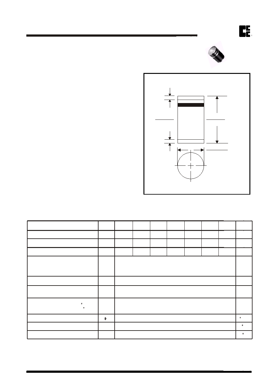
Mechanical data
Case: DO-213AA molded plastic
Terminals: solderable per MIL-STD-750,
method 2026
Polarity: Color band denotes cathode
end
Mounting position: Any
Approx. Weight:0.036 gram
Dimensions in inches and (millimeters)
0.14(3.6)
0.13(3.3)
0.015(0.4)
0.012(0.3)
0.063(1.60)
0.055(1.40)
DO-213AA (Plastic Mini-Melf)
www.comchiptech.com
COMCHIP
COMCHIP

Rating and Characteristic Curves (CGRL0501 Thru CGRL0507)
MDS0212002A
Page 2
SMD Genenal Purpose Rectifier
SMD Genenal Purpose Rectifier
Fig. 1 - Reverse Characteristics
Percent of Rated Peak Reverse Voltage (%)
R
e
v
e
r
s
e
C
u
r
r
e
n
t
(
u
A
)
Fig. 4 - Current Derating Curve
0
0.3
0.6
175
0
25
50
75
100
125 150
A
v
e
r
a
g
e
F
o
r
w
a
r
d
C
u
r
r
e
n
t
(
A
)
0 20 40 60 80 100 120 140
F
o
r
w
a
r
d
C
u
r
r
e
n
t
(
A
)
Forward Voltage (V)
Fig.2 - Forward Characteristics
0.1
0.2
0.5
0.4
P
e
a
k
S
u
r
g
e
F
o
r
w
a
r
d
C
u
r
r
e
n
t
(
A
)
Fig. 5 - Non Repetitive Forward
Surge Current
0
2
4
10
8
6
1 5 10 50 1 00
Number of Cycles at 60Hz
1
100
10
0.1
Fig. 3 - Junction Capacitance
Reverse Voltage (V)
J
u
n
c
t
i
o
n
C
a
p
a
c
i
t
a
n
c
e
(
p
F
)
1 10 100
100
10
1
Single Phase
Half wave 60Hz
Resistive or inductive Load
Ambient Temperature ( C)
Tj=25 C
8.3mS Single Half Sine
Wave JEDEC methode
04 0.6 0.8 1.0 1.2 1.4 1.6
10
1.0
0.1
0.01
Tj=25 C
Pulse width 300uS
1% duty cycle
Tj=25 C
Tj=100 C
=1MHz and applied
Vs0g=50mVp-p
Tj=25 C
www.comchiptech.com
COMCHIP
COMCHIP