 | –≠–ª–µ–∫—Ç—Ä–æ–Ω–Ω—ã–π –∫–æ–º–ø–æ–Ω–µ–Ω—Ç: CN8223 | –°–∫–∞—á–∞—Ç—å:  PDF PDF  ZIP ZIP |

Data Sheet
100046C
March
8, 2000
8223_042
Data
Bus
Port
Control
8
8
UTOPIA
or FIFO
Interface
Cell
FIFO
4-Port
FIFO
Interface
Microprocessor
Interface
52 Control Registers
28 Status Registors
Microprocessor
Address
Microprocessor
Data
Line Overhead
7
8
8
8
8
8
8
8
16
HDLC
Data
Link
Cell
Generation
TX
Rate
Control
Header
Filter
Cell
Validation
Cell
Alignment
HEC or
PLCP
DS3
E3 (G.751)
E3 (G.832)
STS-1
E4 (G.832)
STS-3c
STM-1
TAXI
Framers
1
1
ATM Layer
Physical Framing
ATM
UNI
CN8223
ATM Transmitter/Receiver with UTOPIA Interface
The CN8223 ATM Transmitter/Receiver with UTOPIA Level 1 interface provides a
single-access ATM service termination for User-to-Network (UNI) and
Network-to-Network Interfacing (NNI) in conformance with ATM Forum UNI and NNI
Specification 94/0317; Bellcore Specifications TR-TSV-000772, TR-TSV-000773,
TR-NWT-000253, and T1S1/92-185; ITU Recommendations I.432, G.707, G.751,
G.832, and Q.921; and ETSI prETS 300 213 and 300 214. Both Customer Premise
Equipment (CPE) and switching system interface functions are provided. The CN8223
provides DS1, E1, DS3, E3, E4, STS-1, and STS-3c (and STM-1) ATM cell alignment
functions. The system interface is via a parallel FIFO port or UTOPIA interface. In
addition, the CN8223 terminates the operations and maintenance flows F1, F2, and F3.
The CN8223 provides four FIFO port interfaces and one UTOPIA interface. Each
receiver port can be programmed with a particular Virtual Channel Identifier/Virtual
Path Identifier (VCI/VPI) address for message routing. VCI/VPI pages can also be
selected via masking registers.
The microprocessor can set control registers for insertion of selected header fields
by the transmitter on an individual port basis. The microprocessor can also control
insertion of all overhead and can insert errors in selected fields for test equipment
applications.
Functional Block Diagram
Distinguishing Features
∑
Integrates 7 line framers with ATM
layer processing according to ATM
Forum UNI and NNI Specifications
∑
UTOPIA Level 1 interface
∑
Internal framers for DS3, E3 (G.751,
G.832), E4 (G.832), STS-1, STS-3c,
STM-1
∑
PLCP and G.804 HEC cell alignment
for all data rates from 1.544 Mbps to
155 Mbps
∑
Direct interface to TAXI
TM
or external
T1/E1 framers
∑
ATM and SMDS cell modes
∑
4 FIFO ports with header screening,
formatting, and transmit priority
controls
∑
Idle cells generated and screened
∑
Statistics counts latched on
one-second intervals
∑
Error detection and insertion
∑
Option insertion or generation of all
line and cell overhead
∑
Serial or parallel line interface
∑
Available evaluation module
reference design and software
∑
Supports Automatic Protection
Switching (APS)
Applications
∑
WAN equipment
∑
ATM switches
∑
Test equipment
∑
ATM routers and hub

100046C
Conexant
© 1999, 2000,
Conexant Systems, Inc.
All Rights Reserved.
Information in this document is provided in connection with Conexant Systems, Inc. ("Conexant") products. These materials are
provided by Conexant as a service to its customers and may be used for informational purposes only. Conexant assumes no
responsibility for errors or omissions in these materials. Conexant may make changes to specifications and product descriptions at
any time, without notice. Conexant makes no commitment to update the information and shall have no responsibility whatsoever for
conflicts or incompatibilities arising from future changes to its specifications and product descriptions.
No license, express or implied, by estoppel or otherwise, to any intellectual property rights is granted by this document. Except as
provided in Conexant's Terms and Conditions of Sale for such products, Conexant assumes no liability whatsoever.
THESE MATERIALS ARE PROVIDED "AS IS" WITHOUT WARRANTY OF ANY KIND, EITHER EXPRESS OR IMPLIED, RELATING
TO SALE AND/OR USE OF CONEXANT PRODUCTS INCLUDING LIABILITY OR WARRANTIES RELATING TO FITNESS FOR A
PARTICULAR PURPOSE, CONSEQUENTIAL OR INCIDENTIAL DAMAGES, MERCHANTABILITY, OR INFRINGEMENT OF ANY
PATENT, COPYRIGHT OR OTHER INTELLECTUAL PROPERTY RIGHT. CONEXANT FURTHER DOES NOT WARRANT THE
ACCURACY OR COMPLETENESS OF THE INFORMATION, TEXT, GRAPHICS OR OTHER ITEMS CONTAINED WITHIN THESE
MATERIALS. CONEXANT SHALL NOT BE LIABLE FOR ANY SPECIAL, INDIRECT, INCIDENTAL, OR CONSEQUENTIAL
DAMAGES, INCLUDING WITHOUT LIMITATION, LOST REVENUES OR LOST PROFITS, WHICH MAY RESULT FROM THE USE
OF THESE MATERIALS.
Conexant products are not intended for use in medical, life saving or life sustaining applications. Conexant customers using or selling
Conexant products for use in such applications do so at their own risk and agree to fully indemnify Conexant for any damages
resulting from such improper use or sale.
The following are trademarks of Conexant Systems, Inc.: ConexantTM, the Conexant CTM symbol, and "What's Next in
Communications Technologies"TM. Product names or services listed in this publication are for identification purposes only, and may be
trademarks of third parties. Third-party brands and names are the property of their respective owners.
For additional disclaimer information, please consult Conexant's disclaimer information posted at
www.conexant.com
which is
incorporated by reference.
Reader Response: Conexant strives to produce quality documentation and welcomes your feedback. Please send comments and
suggestions to
conexant.tech.pubs@conexant.com
. For technical questions, contact your local Conexant
sales office
or field
applications engineer.
Ordering Information
Part Number
Generic Part
Number
Operating
Temperature
Package
Description
Reduced Features
28222-13
Bt8222EPFE
≠40
∞
C to 85
∞
C
160-pin PQFP
--
28222-14
Bt8222EPFF
≠40
∞
C to 85
∞
C
160-pin PQFP
--
28233-11
CN8223EPF
≠40
∞
C to 85
∞
C
160-pin PQFP
The CN8223 is based on the Bt8222
device. The only change from the
Bt8222 to the CN8223 is the TTL
I/O pad ring. The I/O structure
allows the CN8223 to function in a
3.3/5 V environment. No new
features, errata fixes, etc., have
been added to the CN8223 other
than TTL threshold inputs.

10046C
Conexant
iii
Table of Contents
List of Figures
. . . . . . . . . . . . . . . . . . . . . . . . . . . . . . . . . . . . . . . . . . . . . . . . . . . . . . . . . . . . . . . . . . . . . . . . vii
List of Tables
. . . . . . . . . . . . . . . . . . . . . . . . . . . . . . . . . . . . . . . . . . . . . . . . . . . . . . . . . . . . . . . . . . . . . . . . . . ix
1.0
Product Description
. . . . . . . . . . . . . . . . . . . . . . . . . . . . . . . . . . . . . . . . . . . . . . . . . . . . . . . . . . . . . 1-1
1.1
Block Diagram
. . . . . . . . . . . . . . . . . . . . . . . . . . . . . . . . . . . . . . . . . . . . . . . . . . . . . . . . . . . . . 1-1
1.2
CN8223 Features
. . . . . . . . . . . . . . . . . . . . . . . . . . . . . . . . . . . . . . . . . . . . . . . . . . . . . . . . . . . . 1-3
1.2.1
Internal Framers
. . . . . . . . . . . . . . . . . . . . . . . . . . . . . . . . . . . . . . . . . . . . . . . . . . . . . . . 1-3
1.2.2
UTOPIA Port
. . . . . . . . . . . . . . . . . . . . . . . . . . . . . . . . . . . . . . . . . . . . . . . . . . . . . . . . . 1-3
1.2.3
Programmable Parity Protection
. . . . . . . . . . . . . . . . . . . . . . . . . . . . . . . . . . . . . . . . . . . 1-4
1.2.4
Test and Diagnostic Functions
. . . . . . . . . . . . . . . . . . . . . . . . . . . . . . . . . . . . . . . . . . . . 1-4
1.2.5
Microprocessor Interface Features
. . . . . . . . . . . . . . . . . . . . . . . . . . . . . . . . . . . . . . . . . 1-4
1.3
Line Framing Functions
. . . . . . . . . . . . . . . . . . . . . . . . . . . . . . . . . . . . . . . . . . . . . . . . . . . . . . 1-5
1.3.1
Interfaces
. . . . . . . . . . . . . . . . . . . . . . . . . . . . . . . . . . . . . . . . . . . . . . . . . . . . . . . . . . . 1-6
1.3.2
Line Loopback
. . . . . . . . . . . . . . . . . . . . . . . . . . . . . . . . . . . . . . . . . . . . . . . . . . . . . . . . 1-6
1.3.3
BIP-8 Code
. . . . . . . . . . . . . . . . . . . . . . . . . . . . . . . . . . . . . . . . . . . . . . . . . . . . . . . . . . 1-7
1.3.4
Alarm Detection/Generation
. . . . . . . . . . . . . . . . . . . . . . . . . . . . . . . . . . . . . . . . . . . . . . 1-7
1.4
ATM Cell Processing Functions
. . . . . . . . . . . . . . . . . . . . . . . . . . . . . . . . . . . . . . . . . . . . . . . . . 1-8
1.4.1
Cell Generation Functions
. . . . . . . . . . . . . . . . . . . . . . . . . . . . . . . . . . . . . . . . . . . . . . . . 1-9
1.4.2
Tx Rate Control
. . . . . . . . . . . . . . . . . . . . . . . . . . . . . . . . . . . . . . . . . . . . . . . . . . . . . . . 1-9
1.4.3
Cell Validation Functions
. . . . . . . . . . . . . . . . . . . . . . . . . . . . . . . . . . . . . . . . . . . . . . . . . 1-9
1.5
FIFO Port/UTOPIA Interface
. . . . . . . . . . . . . . . . . . . . . . . . . . . . . . . . . . . . . . . . . . . . . . . . . . . 1-10
1.5.1
UTOPIA Mode
. . . . . . . . . . . . . . . . . . . . . . . . . . . . . . . . . . . . . . . . . . . . . . . . . . . . . . . 1-10
1.5.2
FIFO Ports
. . . . . . . . . . . . . . . . . . . . . . . . . . . . . . . . . . . . . . . . . . . . . . . . . . . . . . . . . . 1-10
1.5.3
ATM Interface
. . . . . . . . . . . . . . . . . . . . . . . . . . . . . . . . . . . . . . . . . . . . . . . . . . . . . . . 1-11
1.6
Line Interface Applications
. . . . . . . . . . . . . . . . . . . . . . . . . . . . . . . . . . . . . . . . . . . . . . . . . . . 1-12
1.7
CN8223 Versions
. . . . . . . . . . . . . . . . . . . . . . . . . . . . . . . . . . . . . . . . . . . . . . . . . . . . . . . . . . . 1-13
1.8
CN8223 Applications
. . . . . . . . . . . . . . . . . . . . . . . . . . . . . . . . . . . . . . . . . . . . . . . . . . . . . . . . 1-14
1.8.1
CN8223 as a DS3 or E3 G.751 Framer without ATM Cell Delineation
. . . . . . . . . . . . . . . . 1-16
1.9
Logic Diagram
. . . . . . . . . . . . . . . . . . . . . . . . . . . . . . . . . . . . . . . . . . . . . . . . . . . . . . . . . . . . 1-17
1.10 Pin Definitions
. . . . . . . . . . . . . . . . . . . . . . . . . . . . . . . . . . . . . . . . . . . . . . . . . . . . . . . . . . . . 1-19

Table of Contents
CN8223
ATM Transmitter/Receiver with UTOPIA Interface
iv
Conexant
100046C
2.0
Functional Description
. . . . . . . . . . . . . . . . . . . . . . . . . . . . . . . . . . . . . . . . . . . . . . . . . . . . . . . . . . 2-1
2.1
Microprocessor Interface
. . . . . . . . . . . . . . . . . . . . . . . . . . . . . . . . . . . . . . . . . . . . . . . . . . . . . 2-2
2.1.1
8/16-Bit Interface
. . . . . . . . . . . . . . . . . . . . . . . . . . . . . . . . . . . . . . . . . . . . . . . . . . . . . . 2-2
2.1.2
Interrupts
. . . . . . . . . . . . . . . . . . . . . . . . . . . . . . . . . . . . . . . . . . . . . . . . . . . . . . . . . . . . 2-2
2.2
Line Framers
. . . . . . . . . . . . . . . . . . . . . . . . . . . . . . . . . . . . . . . . . . . . . . . . . . . . . . . . . . . . . . 2-3
2.2.1
Internally Framed Transmit Line Interface
. . . . . . . . . . . . . . . . . . . . . . . . . . . . . . . . . . . . 2-4
2.2.1.1
High-Speed PECL Transmit Interface
. . . . . . . . . . . . . . . . . . . . . . . . . . . . . . . 2-5
2.2.2
Internally Framed Receive Line Interface
. . . . . . . . . . . . . . . . . . . . . . . . . . . . . . . . . . . . . 2-6
2.2.2.1
High-Speed PECL Receive Interface
. . . . . . . . . . . . . . . . . . . . . . . . . . . . . . . . 2-7
2.2.2.2
Receiver Framing Operation
. . . . . . . . . . . . . . . . . . . . . . . . . . . . . . . . . . . . . . 2-7
2.2.3
Externally Framed Transmit Line Interface
. . . . . . . . . . . . . . . . . . . . . . . . . . . . . . . . . . . . 2-8
2.2.4
Externally Framed Receive Line Interface
. . . . . . . . . . . . . . . . . . . . . . . . . . . . . . . . . . . . 2-11
2.3
Overhead Generation
. . . . . . . . . . . . . . . . . . . . . . . . . . . . . . . . . . . . . . . . . . . . . . . . . . . . . . . 2-13
2.3.1
Internal DS3 Mode
. . . . . . . . . . . . . . . . . . . . . . . . . . . . . . . . . . . . . . . . . . . . . . . . . . . . 2-13
2.3.2
Internal G.832 E3/E4 Modes
. . . . . . . . . . . . . . . . . . . . . . . . . . . . . . . . . . . . . . . . . . . . . 2-14
2.3.3
Internal G.751 E3 Mode
. . . . . . . . . . . . . . . . . . . . . . . . . . . . . . . . . . . . . . . . . . . . . . . . 2-14
2.3.4
STS-1 and STS-3c/STM-1 Modes
. . . . . . . . . . . . . . . . . . . . . . . . . . . . . . . . . . . . . . . . . 2-15
2.3.5
Transmit Framing Overhead Interface
. . . . . . . . . . . . . . . . . . . . . . . . . . . . . . . . . . . . . . 2-17
2.3.6
Receive Framing Overhead Interface
. . . . . . . . . . . . . . . . . . . . . . . . . . . . . . . . . . . . . . . 2-18
2.4
Status and Alarms
. . . . . . . . . . . . . . . . . . . . . . . . . . . . . . . . . . . . . . . . . . . . . . . . . . . . . . . . . . 2-19
2.4.1
Status and Counter Interrupts
. . . . . . . . . . . . . . . . . . . . . . . . . . . . . . . . . . . . . . . . . . . . 2-19
2.4.2
Alarm Signal Generation
. . . . . . . . . . . . . . . . . . . . . . . . . . . . . . . . . . . . . . . . . . . . . . . . 2-20
2.4.3
Alarm Detection
. . . . . . . . . . . . . . . . . . . . . . . . . . . . . . . . . . . . . . . . . . . . . . . . . . . . . . 2-21
2.5
Parallel Line Interface
. . . . . . . . . . . . . . . . . . . . . . . . . . . . . . . . . . . . . . . . . . . . . . . . . . . . . . 2-22
2.5.1
TAXI Interface
. . . . . . . . . . . . . . . . . . . . . . . . . . . . . . . . . . . . . . . . . . . . . . . . . . . . . . . 2-22
2.5.2
Transmit Parallel Interface
. . . . . . . . . . . . . . . . . . . . . . . . . . . . . . . . . . . . . . . . . . . . . . 2-23
2.5.3
Receive Parallel Interface
. . . . . . . . . . . . . . . . . . . . . . . . . . . . . . . . . . . . . . . . . . . . . . . 2-25
2.6
ATM Cell Processing
. . . . . . . . . . . . . . . . . . . . . . . . . . . . . . . . . . . . . . . . . . . . . . . . . . . . . . . . 2-26
2.6.1
Cell Generation for Transmit
. . . . . . . . . . . . . . . . . . . . . . . . . . . . . . . . . . . . . . . . . . . . . 2-26
2.6.1.1
CELL_GEN_x Register
. . . . . . . . . . . . . . . . . . . . . . . . . . . . . . . . . . . . . . . . . 2-27
2.6.1.2
Cell Generation Status and Status Interrupts for Transmit
. . . . . . . . . . . . . . . 2-28
2.6.2
Cell Validation for Receive
. . . . . . . . . . . . . . . . . . . . . . . . . . . . . . . . . . . . . . . . . . . . . . 2-29
2.6.2.1
HEC Alignment
. . . . . . . . . . . . . . . . . . . . . . . . . . . . . . . . . . . . . . . . . . . . . . 2-30
2.6.2.2
CELL_VAL Control Register
. . . . . . . . . . . . . . . . . . . . . . . . . . . . . . . . . . . . . 2-30
2.6.2.3
Interrupts and Status Counters for Cell Validation
. . . . . . . . . . . . . . . . . . . . . 2-32
2.6.3
PLCP Cell Generation for Transmit
. . . . . . . . . . . . . . . . . . . . . . . . . . . . . . . . . . . . . . . . 2-33
2.6.4
PLCP Cell Validation for Receive
. . . . . . . . . . . . . . . . . . . . . . . . . . . . . . . . . . . . . . . . . . 2-35
2.6.4.1
PLCP Status
. . . . . . . . . . . . . . . . . . . . . . . . . . . . . . . . . . . . . . . . . . . . . . . . 2-35
2.6.5
PLCP Transmit/Receive Synchronization
. . . . . . . . . . . . . . . . . . . . . . . . . . . . . . . . . . . . 2-36

CN8223
Table of Contents
ATM Transmitter/Receiver with UTOPIA Interface
100046C
Conexant
v
2.7
FIFO Port/UTOPIA Interface
. . . . . . . . . . . . . . . . . . . . . . . . . . . . . . . . . . . . . . . . . . . . . . . . . . . 2-37
2.7.1
FIFO Interface Inputs and Outputs
. . . . . . . . . . . . . . . . . . . . . . . . . . . . . . . . . . . . . . . . . 2-37
2.7.2
Transmit Port Priority Mechanism
. . . . . . . . . . . . . . . . . . . . . . . . . . . . . . . . . . . . . . . . . 2-40
2.7.3
Transmit Rate Shaping Control
. . . . . . . . . . . . . . . . . . . . . . . . . . . . . . . . . . . . . . . . . . . 2-41
2.7.4
Receive Port Addressing
. . . . . . . . . . . . . . . . . . . . . . . . . . . . . . . . . . . . . . . . . . . . . . . . 2-41
2.7.4.1
Header Screening
. . . . . . . . . . . . . . . . . . . . . . . . . . . . . . . . . . . . . . . . . . . . 2-42
2.7.4.2
Output Screening
. . . . . . . . . . . . . . . . . . . . . . . . . . . . . . . . . . . . . . . . . . . . 2-42
2.7.5
UTOPIA Interface
. . . . . . . . . . . . . . . . . . . . . . . . . . . . . . . . . . . . . . . . . . . . . . . . . . . . . 2-43
2.8
FEAC Channel and HDLC Data Link Programming
. . . . . . . . . . . . . . . . . . . . . . . . . . . . . . . . . . 2-44
2.8.1
FEAC Channel Transmitter
. . . . . . . . . . . . . . . . . . . . . . . . . . . . . . . . . . . . . . . . . . . . . . 2-44
2.8.2
FEAC Channel Receiver
. . . . . . . . . . . . . . . . . . . . . . . . . . . . . . . . . . . . . . . . . . . . . . . . . 2-45
2.8.3
HDLC Data Link Transmitter
. . . . . . . . . . . . . . . . . . . . . . . . . . . . . . . . . . . . . . . . . . . . . 2-45
2.8.3.1
Sending a Message
. . . . . . . . . . . . . . . . . . . . . . . . . . . . . . . . . . . . . . . . . . . 2-46
2.8.3.2
Aborting a Message
. . . . . . . . . . . . . . . . . . . . . . . . . . . . . . . . . . . . . . . . . . 2-47
2.8.3.3
Transmitter Interrupts
. . . . . . . . . . . . . . . . . . . . . . . . . . . . . . . . . . . . . . . . . 2-47
2.8.3.4
Transmitter Control Example
. . . . . . . . . . . . . . . . . . . . . . . . . . . . . . . . . . . . 2-48
2.8.4
HDLC Data Link Receiver
. . . . . . . . . . . . . . . . . . . . . . . . . . . . . . . . . . . . . . . . . . . . . . . 2-48
2.8.4.1
Receiver Operation
. . . . . . . . . . . . . . . . . . . . . . . . . . . . . . . . . . . . . . . . . . . 2-49
2.8.4.2
Receiver Interrupts
. . . . . . . . . . . . . . . . . . . . . . . . . . . . . . . . . . . . . . . . . . . 2-50
2.8.5
Receiver Response Example
. . . . . . . . . . . . . . . . . . . . . . . . . . . . . . . . . . . . . . . . . . . . . 2-51
3.0
Registers
. . . . . . . . . . . . . . . . . . . . . . . . . . . . . . . . . . . . . . . . . . . . . . . . . . . . . . . . . . . . . . . . . . . . . . 3-1
3.1
Registers Overview
. . . . . . . . . . . . . . . . . . . . . . . . . . . . . . . . . . . . . . . . . . . . . . . . . . . . . . . . . . 3-1
3.2
Control Register Overview
. . . . . . . . . . . . . . . . . . . . . . . . . . . . . . . . . . . . . . . . . . . . . . . . . . . . 3-2
3.3
Configuration Control Registers
. . . . . . . . . . . . . . . . . . . . . . . . . . . . . . . . . . . . . . . . . . . . . . . . 3-4
0x00--CONFIG_1 (Configuration Control Register 1) . . . . . . . . . . . . . . . . . . . . . . . . . . . . . . . . . . . . 3-4
0x01--CONFIG_2 (Configuration Control Register 2) . . . . . . . . . . . . . . . . . . . . . . . . . . . . . . . . . . . . 3-7
0x02--CONFIG_3 (Configuration Control Register 3) . . . . . . . . . . . . . . . . . . . . . . . . . . . . . . . . . . . . 3-9
0x29--CONFIG_4 (Configuration Control Register 4) . . . . . . . . . . . . . . . . . . . . . . . . . . . . . . . . . . . 3-10
0x31--CONFIG_5 (Configuration Control Register 5) . . . . . . . . . . . . . . . . . . . . . . . . . . . . . . . . . . . 3-11
0x2B--UTOPIA_1 (Utopia Port Control Register 1). . . . . . . . . . . . . . . . . . . . . . . . . . . . . . . . . . . . . 3-12
0x2C--UTOPIA_2 (Utopia Port Control Register 2). . . . . . . . . . . . . . . . . . . . . . . . . . . . . . . . . . . . . 3-13
3.4
Transmit Control Registers
. . . . . . . . . . . . . . . . . . . . . . . . . . . . . . . . . . . . . . . . . . . . . . . . . . . 3-14
0x03--TXFEAC_ERRPAT (Transmit FEAC/Error Pattern Register) . . . . . . . . . . . . . . . . . . . . . . . . . 3-14
0x60--DL_CTRL_STAT (HDLC Data Link Control and Status Register) . . . . . . . . . . . . . . . . . . . . . 3-15
0x04≠0x07--CELL_GEN_x (Cell Generation Control Registers) . . . . . . . . . . . . . . . . . . . . . . . . . . . 3-16
0x08--TX_RATE_23 (Transmit Rate Control Register) . . . . . . . . . . . . . . . . . . . . . . . . . . . . . . . . . . 3-17
0x09--TX_RATE_01 (Transmit Rate Control Register) . . . . . . . . . . . . . . . . . . . . . . . . . . . . . . . . . . 3-17
0x0A--TX_IDLE_12 (Transmit Idle Header Register) . . . . . . . . . . . . . . . . . . . . . . . . . . . . . . . . . . . 3-17
0x0B--TX_IDLE_34 (Transmit Idle Header Register) . . . . . . . . . . . . . . . . . . . . . . . . . . . . . . . . . . . 3-17
0x2A--IDLE_PAY (Transmit Idle Cell Payload Register) . . . . . . . . . . . . . . . . . . . . . . . . . . . . . . . . . 3-18
0x0C≠0x13--TX_HDRx_12, TX_HDRx_34 (Transmit Header Registers) . . . . . . . . . . . . . . . . . . . . 3-18

Table of Contents
CN8223
ATM Transmitter/Receiver with UTOPIA Interface
vi
Conexant
100046C
3.5
Receive Control Registers
. . . . . . . . . . . . . . . . . . . . . . . . . . . . . . . . . . . . . . . . . . . . . . . . . . . . 3-19
0x14--CELL_VAL (Cell Validation Control Register) . . . . . . . . . . . . . . . . . . . . . . . . . . . . . . . . . . . . 3-19
0x15≠0x1C--HDR_VALx_12, HDR_VALx_34 (Receive Header Value Register) . . . . . . . . . . . . . . . 3-21
0x1D≠0x24--HDR_MSKx_12, HDR_MSKx_34 (Receive Header Mask Register) . . . . . . . . . . . . . . 3-22
0x25, 0x26--RX_IDLE_12, RX_IDLE_34 (Receive Idle Header Registers) . . . . . . . . . . . . . . . . . . . 3-23
0x27, 0x28--IDLE_MSK_12, IDLE_MSK_34 (Receive Idle Header Mask Register) . . . . . . . . . . . . 3-23
3.6
Interrupt Enable Control Registers
. . . . . . . . . . . . . . . . . . . . . . . . . . . . . . . . . . . . . . . . . . . . . 3-24
0x2D--EN_LINE_INT (Enable Line Interrupts) . . . . . . . . . . . . . . . . . . . . . . . . . . . . . . . . . . . . . . . . 3-24
0x2E--EN_EVENT_INT (Enable Event Interrupts) . . . . . . . . . . . . . . . . . . . . . . . . . . . . . . . . . . . . . . 3-25
0x2F--EN_OVFL_INT (Enable Overflow Interrupts). . . . . . . . . . . . . . . . . . . . . . . . . . . . . . . . . . . . . 3-26
0x30--EN_CELL_INT (Enable Cell Interrupts) . . . . . . . . . . . . . . . . . . . . . . . . . . . . . . . . . . . . . . . . . 3-27
0x32--TX_K1K2 (Transmit K1 and K2 Value) . . . . . . . . . . . . . . . . . . . . . . . . . . . . . . . . . . . . . . . . . 3-27
0x33--RX_K1K2 (Receive K1 and K2 value) . . . . . . . . . . . . . . . . . . . . . . . . . . . . . . . . . . . . . . . . . . 3-27
3.7
Status Register Overview
. . . . . . . . . . . . . . . . . . . . . . . . . . . . . . . . . . . . . . . . . . . . . . . . . . . . 3-28
0x38--LINE_STATUS (Line Framer/PHY Interrupt Status Register) . . . . . . . . . . . . . . . . . . . . . . . . 3-29
0x39--EVENT_STATUS (Event Interrupt Status Register). . . . . . . . . . . . . . . . . . . . . . . . . . . . . . . . 3-36
0x3A--OVFL_STATUS (Counter Overflow Interrupt Status Register) . . . . . . . . . . . . . . . . . . . . . . . 3-37
0x3B--CELL_STATUS (Interrupt Status Register). . . . . . . . . . . . . . . . . . . . . . . . . . . . . . . . . . . . . . 3-38
0x3C--RXFEAC_VER (Receive FEAC/Part Number/Version Number Register) . . . . . . . . . . . . . . . . 3-38
3.8
Event/Error Counters
. . . . . . . . . . . . . . . . . . . . . . . . . . . . . . . . . . . . . . . . . . . . . . . . . . . . . . . . 3-39
4.0
Electrical and Mechanical Specifications
. . . . . . . . . . . . . . . . . . . . . . . . . . . . . . . . . . . . . . . . . 4-1
4.1
Power Requirements and Temperature Range
. . . . . . . . . . . . . . . . . . . . . . . . . . . . . . . . . . . . . 4-1
4.2
DC Characteristics
. . . . . . . . . . . . . . . . . . . . . . . . . . . . . . . . . . . . . . . . . . . . . . . . . . . . . . . . . . 4-2
4.3
Timing
. . . . . . . . . . . . . . . . . . . . . . . . . . . . . . . . . . . . . . . . . . . . . . . . . . . . . . . . . . . . . . . . . . . 4-4
4.3.1
Microprocessor Interface Timing
. . . . . . . . . . . . . . . . . . . . . . . . . . . . . . . . . . . . . . . . . . 4-4
4.3.2
Line Interface Timing
. . . . . . . . . . . . . . . . . . . . . . . . . . . . . . . . . . . . . . . . . . . . . . . . . . . 4-6
4.3.3
FIFO Interface Timing
. . . . . . . . . . . . . . . . . . . . . . . . . . . . . . . . . . . . . . . . . . . . . . . . . . 4-11
4.3.4
UTOPIA Interface Timing
. . . . . . . . . . . . . . . . . . . . . . . . . . . . . . . . . . . . . . . . . . . . . . . 4-13
4.3.5
TAXI Interface Timing
. . . . . . . . . . . . . . . . . . . . . . . . . . . . . . . . . . . . . . . . . . . . . . . . . . 4-15
4.4
Mechanical Drawing
. . . . . . . . . . . . . . . . . . . . . . . . . . . . . . . . . . . . . . . . . . . . . . . . . . . . . . . . 4-17
Appendix A:Transmit FIFO Port Rates
. . . . . . . . . . . . . . . . . . . . . . . . . . . . . . . . . . . . . . . . . . . . . . . . . . A-1
A.1
Rate Control
. . . . . . . . . . . . . . . . . . . . . . . . . . . . . . . . . . . . . . . . . . . . . . . . . . . . . . . . . . . . . . . A-1
A.2
Port Priority
. . . . . . . . . . . . . . . . . . . . . . . . . . . . . . . . . . . . . . . . . . . . . . . . . . . . . . . . . . . . . . . A-2
A.3
Summary
. . . . . . . . . . . . . . . . . . . . . . . . . . . . . . . . . . . . . . . . . . . . . . . . . . . . . . . . . . . . . . . . . A-2
Appendix B:Acronym List
. . . . . . . . . . . . . . . . . . . . . . . . . . . . . . . . . . . . . . . . . . . . . . . . . . . . . . . . . . . . . . B-1

CN8223
List of Figures
ATM Transmitter/Receiver with UTOPIA Interface
100046C
Conexant
vii
List of Figures
Figure 1-1.
CN8223 Detailed Block Diagram . . . . . . . . . . . . . . . . . . . . . . . . . . . . . . . . . . . . . . . . . . . . . 1-2
Figure 1-2.
Line Framer Diagram. . . . . . . . . . . . . . . . . . . . . . . . . . . . . . . . . . . . . . . . . . . . . . . . . . . . . . 1-5
Figure 1-3.
CN8223 Cell Processing Block . . . . . . . . . . . . . . . . . . . . . . . . . . . . . . . . . . . . . . . . . . . . . . 1-8
Figure 1-4.
FIFO Port/UTOPIA Interface Block . . . . . . . . . . . . . . . . . . . . . . . . . . . . . . . . . . . . . . . . . . . 1-10
Figure 1-5.
Line Interface Applications . . . . . . . . . . . . . . . . . . . . . . . . . . . . . . . . . . . . . . . . . . . . . . . . 1-12
Figure 1-6.
CN8223 Connected to CAT 5 or PMD . . . . . . . . . . . . . . . . . . . . . . . . . . . . . . . . . . . . . . . . 1-14
Figure 1-7.
CN8223 Connected to Bt8360 . . . . . . . . . . . . . . . . . . . . . . . . . . . . . . . . . . . . . . . . . . . . . . 1-14
Figure 1-8.
CN8223 Connected to Bt8510 . . . . . . . . . . . . . . . . . . . . . . . . . . . . . . . . . . . . . . . . . . . . . . 1-15
Figure 1-9.
CN8223 Connected to Bt8370 . . . . . . . . . . . . . . . . . . . . . . . . . . . . . . . . . . . . . . . . . . . . . . 1-15
Figure 1-10.
CN8223 Connected to TDK 78P7200. . . . . . . . . . . . . . . . . . . . . . . . . . . . . . . . . . . . . . . . . 1-16
Figure 1-11.
CN8223 Logic Diagram . . . . . . . . . . . . . . . . . . . . . . . . . . . . . . . . . . . . . . . . . . . . . . . . . . . 1-18
Figure 1-12.
CN8223 Pinout Diagram . . . . . . . . . . . . . . . . . . . . . . . . . . . . . . . . . . . . . . . . . . . . . . . . . . 1-19
Figure 2-1.
CN8223 Receiver Block Diagram. . . . . . . . . . . . . . . . . . . . . . . . . . . . . . . . . . . . . . . . . . . . . 2-1
Figure 2-2.
CN8223 Transmitter Block Diagram . . . . . . . . . . . . . . . . . . . . . . . . . . . . . . . . . . . . . . . . . . 2-1
Figure 2-3.
Internal Framer Transmitter Interface Timing with Line Encoding . . . . . . . . . . . . . . . . . . . . 2-4
Figure 2-4.
Internal Framer Transmitter Interface Timing Without Line Encoding . . . . . . . . . . . . . . . . . 2-5
Figure 2-5.
Internal Framer Receiver Interface Timing. . . . . . . . . . . . . . . . . . . . . . . . . . . . . . . . . . . . . . 2-6
Figure 2-6.
Timing for Internal Framer Receiver, Encoder Disabled . . . . . . . . . . . . . . . . . . . . . . . . . . . 2-7
Figure 2-7.
DS1 Interface Transmit Timing . . . . . . . . . . . . . . . . . . . . . . . . . . . . . . . . . . . . . . . . . . . . . . 2-8
Figure 2-8.
E1 Interface Transmit Timing . . . . . . . . . . . . . . . . . . . . . . . . . . . . . . . . . . . . . . . . . . . . . . . 2-9
Figure 2-9.
DS3 Interface Transmit Timing . . . . . . . . . . . . . . . . . . . . . . . . . . . . . . . . . . . . . . . . . . . . . 2-10
Figure 2-10.
E3 Interface Transmit Timing . . . . . . . . . . . . . . . . . . . . . . . . . . . . . . . . . . . . . . . . . . . . . . 2-11
Figure 2-11.
Receiver DS1 Line Interface Timing . . . . . . . . . . . . . . . . . . . . . . . . . . . . . . . . . . . . . . . . . 2-12
Figure 2-12.
Transmit Framing Overhead Interface Timing . . . . . . . . . . . . . . . . . . . . . . . . . . . . . . . . . . 2-17
Figure 2-13.
Receive Framing Overhead Interface Timing . . . . . . . . . . . . . . . . . . . . . . . . . . . . . . . . . . . 2-18
Figure 2-14.
Transmit Parallel Interface Timing. . . . . . . . . . . . . . . . . . . . . . . . . . . . . . . . . . . . . . . . . . . 2-24
Figure 2-15.
Receive Parallel Interface Timing . . . . . . . . . . . . . . . . . . . . . . . . . . . . . . . . . . . . . . . . . . . 2-25
Figure 2-16.
Transmit FIFO Port Interface Timing, 53-Octet Mode . . . . . . . . . . . . . . . . . . . . . . . . . . . . 2-38
Figure 2-17.
Receive FIFO Port Interface Timing, 53-Octet Mode . . . . . . . . . . . . . . . . . . . . . . . . . . . . . 2-39
Figure 3-1.
LINE_STATUS and OOF Example . . . . . . . . . . . . . . . . . . . . . . . . . . . . . . . . . . . . . . . . . . . 3-29
Figure 3-2.
Register Summary, Cheat Sheet 1. . . . . . . . . . . . . . . . . . . . . . . . . . . . . . . . . . . . . . . . . . . 3-46
Figure 3-3.
Register Summary, Cheat Sheet 2. . . . . . . . . . . . . . . . . . . . . . . . . . . . . . . . . . . . . . . . . . . 3-47
Figure 4-1.
Local Processor Interface Timing . . . . . . . . . . . . . . . . . . . . . . . . . . . . . . . . . . . . . . . . . . . . 4-5
Figure 4-2.
Line Interface Timing--DS1, E1, DS3, E3 External Framers . . . . . . . . . . . . . . . . . . . . . . . . 4-7
Figure 4-3.
Line Interface Timing≠Internal Framers. . . . . . . . . . . . . . . . . . . . . . . . . . . . . . . . . . . . . . . . 4-8
Figure 4-4.
Parallel Interface Timing . . . . . . . . . . . . . . . . . . . . . . . . . . . . . . . . . . . . . . . . . . . . . . . . . . . 4-9
Figure 4-5.
Overhead Port Interface Timing. . . . . . . . . . . . . . . . . . . . . . . . . . . . . . . . . . . . . . . . . . . . . 4-10

List of Figures
CN8223
ATM Transmitter/Receiver with UTOPIA Interface
viii
Conexant
100046C
Figure 4-6.
FIFO Port Interface Timing . . . . . . . . . . . . . . . . . . . . . . . . . . . . . . . . . . . . . . . . . . . . . . . . 4-12
Figure 4-7.
UTOPIA Interface Timing. . . . . . . . . . . . . . . . . . . . . . . . . . . . . . . . . . . . . . . . . . . . . . . . . . 4-14
Figure 4-8.
TAXI Port Interface Timing . . . . . . . . . . . . . . . . . . . . . . . . . . . . . . . . . . . . . . . . . . . . . . . . 4-16
Figure 4-9.
CN8223 160-Pin Plastic Quad Flat Pack . . . . . . . . . . . . . . . . . . . . . . . . . . . . . . . . . . . . . . 4-17

CN8223
List of Tables
ATM Transmitter/Receiver with UTOPIA Interface
100046C
Conexant
ix
List of Tables
Table 1-1.
CN8223 Version Descriptions . . . . . . . . . . . . . . . . . . . . . . . . . . . . . . . . . . . . . . . . . . . . . . . 1-13
Table 1-2.
Hardware Signal Definitions . . . . . . . . . . . . . . . . . . . . . . . . . . . . . . . . . . . . . . . . . . . . . . . . 1-20
Table 2-1.
Valid CONFIG_1 Line Mode Settings, Bits 7≠0 . . . . . . . . . . . . . . . . . . . . . . . . . . . . . . . . . . 2-3
Table 2-2.
Internal Framer Transmitter Interface Connections. . . . . . . . . . . . . . . . . . . . . . . . . . . . . . . . 2-4
Table 2-3.
Internal Framing Unencoded Transmitter Connections (STS-3c, STM-1, E4) . . . . . . . . . . . 2-5
Table 2-4.
Internal Framer Receiver Interface Connections . . . . . . . . . . . . . . . . . . . . . . . . . . . . . . . . . 2-6
Table 2-5.
Connections for Internal Framer Rx, Encoder Disabled (STS-3c, STM-1, E4) . . . . . . . . . . . 2-7
Table 2-6.
Serial External Framer Transmitter Interface Connection . . . . . . . . . . . . . . . . . . . . . . . . . . . 2-8
Table 2-7.
External Framing Mode Receiver Connections . . . . . . . . . . . . . . . . . . . . . . . . . . . . . . . . . 2-11
Table 2-8.
DS3 Overhead Values . . . . . . . . . . . . . . . . . . . . . . . . . . . . . . . . . . . . . . . . . . . . . . . . . . . . 2-13
Table 2-9.
G.832 E3 and E4 Overhead Values . . . . . . . . . . . . . . . . . . . . . . . . . . . . . . . . . . . . . . . . . . 2-14
Table 2-10.
G.751 E3 Overhead Values . . . . . . . . . . . . . . . . . . . . . . . . . . . . . . . . . . . . . . . . . . . . . . . . 2-14
Table 2-11.
C1 Values . . . . . . . . . . . . . . . . . . . . . . . . . . . . . . . . . . . . . . . . . . . . . . . . . . . . . . . . . . . . . . 2-15
Table 2-12.
STS-1, STS-3c, and STM-1 Overhead Values . . . . . . . . . . . . . . . . . . . . . . . . . . . . . . . . . . 2-15
Table 2-13.
Status Indications for All Modes (Register 0x38) . . . . . . . . . . . . . . . . . . . . . . . . . . . . . . . . 2-21
Table 2-14.
Pin Connections between TAXI Chipset and CN8223 . . . . . . . . . . . . . . . . . . . . . . . . . . . . 2-23
Table 2-15.
Transmit Parallel Interface Mode Connections . . . . . . . . . . . . . . . . . . . . . . . . . . . . . . . . . . 2-23
Table 2-16.
Receive Parallel Interface Mode Connections . . . . . . . . . . . . . . . . . . . . . . . . . . . . . . . . . . 2-25
Table 2-17.
Cell Generation Modes . . . . . . . . . . . . . . . . . . . . . . . . . . . . . . . . . . . . . . . . . . . . . . . . . . . . 2-27
Table 2-18.
Overhead Field Locations . . . . . . . . . . . . . . . . . . . . . . . . . . . . . . . . . . . . . . . . . . . . . . . . . . 2-28
Table 2-19.
Status Octet Definition . . . . . . . . . . . . . . . . . . . . . . . . . . . . . . . . . . . . . . . . . . . . . . . . . . . . 2-31
Table 2-20.
PT Header Field and User Data Bit . . . . . . . . . . . . . . . . . . . . . . . . . . . . . . . . . . . . . . . . . . 2-31
Table 2-21.
FEBE Controls . . . . . . . . . . . . . . . . . . . . . . . . . . . . . . . . . . . . . . . . . . . . . . . . . . . . . . . . . . 2-34
Table 2-22.
C1 Octet . . . . . . . . . . . . . . . . . . . . . . . . . . . . . . . . . . . . . . . . . . . . . . . . . . . . . . . . . . . . . . . 2-34
Table 2-23.
FIFO Interface Pin Connections . . . . . . . . . . . . . . . . . . . . . . . . . . . . . . . . . . . . . . . . . . . . . 2-37
Table 2-24.
FIFO Transmit Pin Functional Descriptions . . . . . . . . . . . . . . . . . . . . . . . . . . . . . . . . . . . . 2-39
Table 2-25.
FIFO Receive Pin Descriptions. . . . . . . . . . . . . . . . . . . . . . . . . . . . . . . . . . . . . . . . . . . . . . 2-40
Table 2-26.
Priority Levels . . . . . . . . . . . . . . . . . . . . . . . . . . . . . . . . . . . . . . . . . . . . . . . . . . . . . . . . . . . 2-40
Table 2-27.
UTOPIA Interface Pins . . . . . . . . . . . . . . . . . . . . . . . . . . . . . . . . . . . . . . . . . . . . . . . . . . . . 2-43
Table 2-28.
Byte Transmission Times for Transmitter . . . . . . . . . . . . . . . . . . . . . . . . . . . . . . . . . . . . . . 2-46
Table 3-1.
ATM Transmitter/Receiver Status Registers, Counters, and Data Link Control . . . . . . . . . . 3-1
Table 3-2.
ATM Transmitter/Receiver Microprocessor Control Registers . . . . . . . . . . . . . . . . . . . . . . . 3-2
Table 3-3.
Valid Combinations of CONFIG_1, Bits 0≠7 . . . . . . . . . . . . . . . . . . . . . . . . . . . . . . . . . . . . . 3-6
Table 3-4.
Alarm Transmission . . . . . . . . . . . . . . . . . . . . . . . . . . . . . . . . . . . . . . . . . . . . . . . . . . . . . . . 3-8
Table 3-5.
Alarm Transmission--STS≠1/STS≠3c/STM≠1 . . . . . . . . . . . . . . . . . . . . . . . . . . . . . . . . . . . 3-8
Table 3-6.
Overhead Generation Disable . . . . . . . . . . . . . . . . . . . . . . . . . . . . . . . . . . . . . . . . . . . . . . . 3-8
Table 3-7.
CELL_GEN_x Control Register Addresses . . . . . . . . . . . . . . . . . . . . . . . . . . . . . . . . . . . . 3-16
Table 3-8.
Tx_HDRx Register Addresses . . . . . . . . . . . . . . . . . . . . . . . . . . . . . . . . . . . . . . . . . . . . . . 3-18
Table 3-9.
HDR_VALx Register Addresses . . . . . . . . . . . . . . . . . . . . . . . . . . . . . . . . . . . . . . . . . . . . . 3-21

List of Tables
CN8223
ATM Transmitter/Receiver with UTOPIA Interface
x
Conexant
10046C
Table 3-10.
HDR_MSKx Register Addresses . . . . . . . . . . . . . . . . . . . . . . . . . . . . . . . . . . . . . . . . . . . . 3-22
Table 3-11.
ATM Transmitter/Receiver Status Registers, Counters, and Data Link Control . . . . . . . . . 3-28
Table 3-12.
STS-1,STS-3c, STM-1 LINE_STATUS Bit Definitions. . . . . . . . . . . . . . . . . . . . . . . . . . . . . 3-30
Table 3-13.
DS3 PLCP and Direct Mapping Mode LINE_STATUS Bit Definitions . . . . . . . . . . . . . . . . . 3-31
Table 3-14.
E3 G.832, E4 G.832 LINE_STATUS Bit Definitions . . . . . . . . . . . . . . . . . . . . . . . . . . . . . . 3-32
Table 3-15.
E3 G.751 LINE_STATUS Bit Definitions . . . . . . . . . . . . . . . . . . . . . . . . . . . . . . . . . . . . . . . 3-33
Table 3-16.
External Framer, 57-Octet Mode, LINE_STATUS Bit Definitions . . . . . . . . . . . . . . . . . . . . 3-34
Table 3-17.
Status Indications for All Modes . . . . . . . . . . . . . . . . . . . . . . . . . . . . . . . . . . . . . . . . . . . . . 3-35
Table 3-18.
Line and Interface Events/Errors Counters. . . . . . . . . . . . . . . . . . . . . . . . . . . . . . . . . . . . . 3-39
Table 3-19.
Counted Events . . . . . . . . . . . . . . . . . . . . . . . . . . . . . . . . . . . . . . . . . . . . . . . . . . . . . . . . . 3-40
Table 3-20.
Internal STS-1, STS-3c Event/Error Counters . . . . . . . . . . . . . . . . . . . . . . . . . . . . . . . . . . 3-41
Table 3-21.
Internal DS3 PLCP and Direct Mapping Modes Event/Error Counters. . . . . . . . . . . . . . . . 3-42
Table 3-22.
Internal G.832 E3/E4 Event/Error Counters . . . . . . . . . . . . . . . . . . . . . . . . . . . . . . . . . . . . 3-43
Table 3-23.
Internal G.751 E3 Event/Error Counters. . . . . . . . . . . . . . . . . . . . . . . . . . . . . . . . . . . . . . . 3-44
Table 3-24.
External Framer, 57-Octet Mode Event/Error Counters . . . . . . . . . . . . . . . . . . . . . . . . . . . 3-45
Table 4-1.
DC Characteristics . . . . . . . . . . . . . . . . . . . . . . . . . . . . . . . . . . . . . . . . . . . . . . . . . . . . . . . . 4-3
Table 4-2.
Microprocessor Interface Timing. . . . . . . . . . . . . . . . . . . . . . . . . . . . . . . . . . . . . . . . . . . . . . 4-4
Table 4-3.
Line Interface Timing--DS1, E1, DS3, E3 External Framers . . . . . . . . . . . . . . . . . . . . . . . . 4-6
Table 4-4.
Line Interface Timing--Internal Framers . . . . . . . . . . . . . . . . . . . . . . . . . . . . . . . . . . . . . . . 4-7
Table 4-5.
Parallel Interface Timing . . . . . . . . . . . . . . . . . . . . . . . . . . . . . . . . . . . . . . . . . . . . . . . . . . . . 4-8
Table 4-6.
Overhead Port Interface Timing . . . . . . . . . . . . . . . . . . . . . . . . . . . . . . . . . . . . . . . . . . . . . . 4-9
Table 4-7.
FIFO Port Interface Timing . . . . . . . . . . . . . . . . . . . . . . . . . . . . . . . . . . . . . . . . . . . . . . . . . 4-11
Table 4-8.
UTOPIA Interface Timing . . . . . . . . . . . . . . . . . . . . . . . . . . . . . . . . . . . . . . . . . . . . . . . . . . 4-13
Table 4-9.
TAXI Interface Timing . . . . . . . . . . . . . . . . . . . . . . . . . . . . . . . . . . . . . . . . . . . . . . . . . . . . . 4-15
Table A-1.
Cell Thresholds (1 of 4) . . . . . . . . . . . . . . . . . . . . . . . . . . . . . . . . . . . . . . . . . . . . . . . . . . . . A-3

100046C
Conexant
1-1
1
1.0 Product Description
The CN8223 ATM Physical Interface (PHY) device is a transmitter/receiver
which converts several types of frames to ATM cells and vice versa. The device
contains framers for DS3, E3, E4, STS-1, STS-3c, and STM-1. This chapter
provides an overview of the CN8223, describing its primary features and
applications. A block diagram and a logic diagram are included.
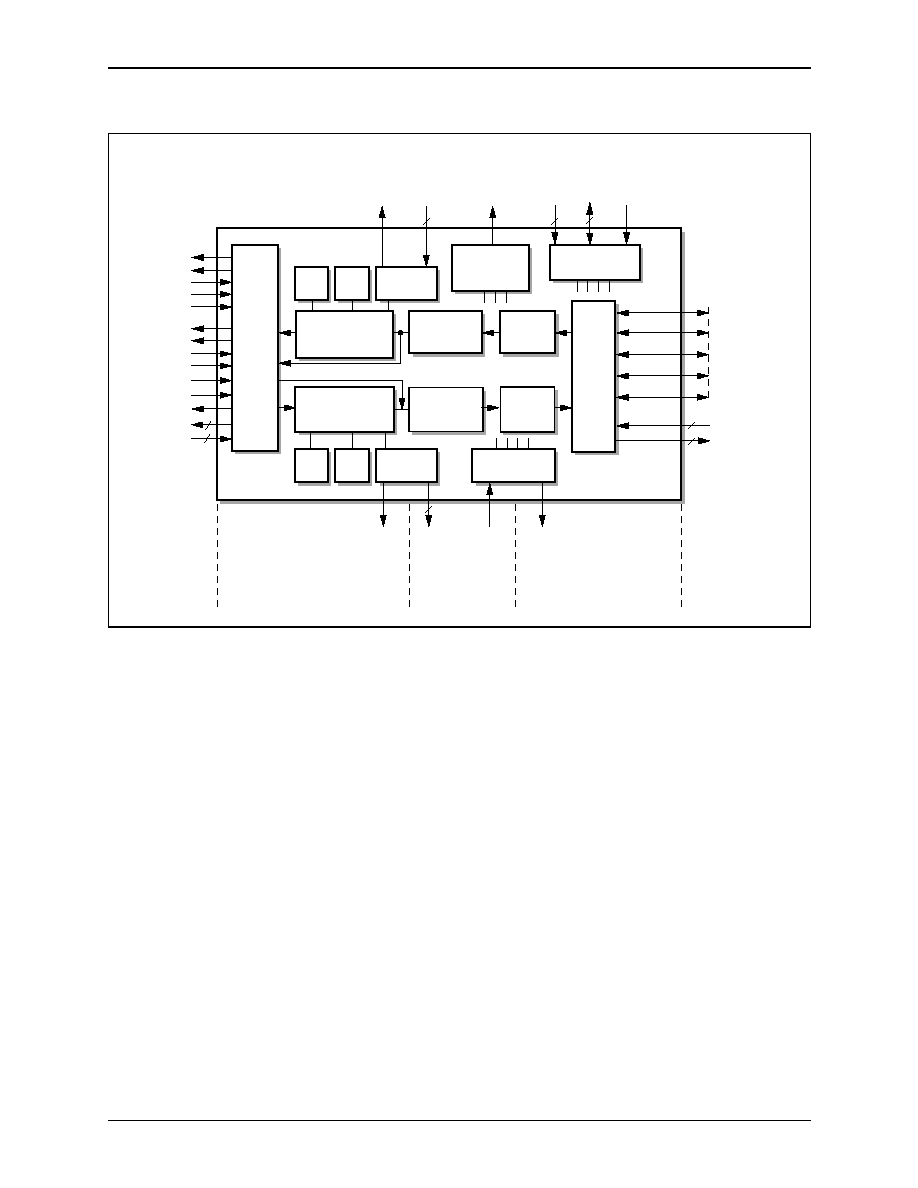
1.1 Block Diagram
Figure 1-1
is a detailed block diagram of the CN8223. The host system transmits
octet-wide data to the CN8223 via the UTOPIA or FIFO ports. This data is
assembled into ATM cells by the PHY and formatted for serial line transmission
by the CN8223's line framers. In the receive direction, serial network data is
framed into octets by either internal or external line framers and passed to the
ATM cell processing block. Octet data is then aligned into ATM cells, checked,
and sent through the UTOPIA or FIFO ports to the host system.
The line framer block connects to external interfaces for line reception and
transmission. The line framer has interfaces for seven data rates and provisions
for external serial or parallel framers. Also included are overhead interfaces, data
links, and event counters.
The HEC/PLCP ATM cell alignment block accepts octet data from the line
framer block. It generates cells for transmission and validates received cells.
Included are HEC/PLCP generators and detectors, data scramblers, and counters.
The FIFO Port/UTOPIA interface communicates with the next layer of ATM
processing, usually residing in the host system. It directs received cell traffic to
four ports, controls transmit priority and rate, and has counters for events and
errors.
1.0 Product Description
CN8223
1.1 Block Diagram
ATM Transmitter/Receiver with UTOPIA Interface
1-2
Conexant
100046C
Figure 1-1. CN8223 Detailed Block Diagram
Port 1 Ctrl
Port 2 Ctrl
Port 3 Ctrl
UTOPIA Ctrl
Port 0 Ctrl
DS3, E3, E4, STS-1
STS-3c, STM-1
G.832
Transmit Framer
DS3, E3, E4, STS-1
STS-3c, STM-1
G.832
Receive Framer
Microprocessor
Interface
Transmit G.832
and PLCP
Framer
Rx
HDLC
Tx
FEAC
Tx
HDLC
Tx Cell
Generation,
Tx Rate
and Priority
Rx Cell
Validation
Rx VPI/VCI
Screening
4-Port
FIFO
Data
Interface
9
9
Tx
Overhead
Insert
Rx
Overhead
Extract
Line
Interfaces
9
9
Parallel
Interface
High
Speed
Medium
Speed
8
RXOVH
TXOVH
RMRKR
ROVH_CLK
TMRKR
TOVH_CLK
A[7:1]
PRCLK
CS~
AS~
W/R~
OE~
SEL8BIT
FDAT_IN
FDAT_OUT
FCTRL_OUT[16:0]
TCLKO_HS
±
TCLKO
TXOUT[7:0]
RCV_HLD
Clock and
Control
ONESECI
8KCKI
NTEST
TEST1, 3
RESET
Line Framer Section
Cell Processing
Section
FIFO Data Ports Section
16
TXOUT_HS
±
TXCKI_HS
±
RXCKI_HS
±
RXIN_HS
±
TXOUT
TXCKI
RXCKI
RXIN
LOCD
RXIN[7:0]
Receive G.832
and PLCP
Framer
8
UTOPIA
Interface
and
4-Cell
Buffers
Rx
FEAC
8
FCTRL_IN[7:0]
Cell Counters
Performance
Monitoring
Interrupt Control
CN8223
DL_INT
STAT_INT
D[15:0]
ONESECO
8223_001

CN8223
1.0 Product Description
ATM Transmitter/Receiver with UTOPIA Interface
1.2 CN8223 Features
100046C
Conexant
1-3
1.2 CN8223 Features
The CN8223 ATM Transmitter/Receiver provides a single-access ATM service
termination for UNI and NNI. It conforms to the following specifications and
recommendations:
∑
ATM Forum UNI Specification 94/0317
∑
Bellcore Specifications TR-TSV-000772, TR-TSV-000773,
TR-NWT-000253, and T1S1/92-185
∑
ITU Recommendations I.432, G.707, G.751, G.832, and Q.921
∑
ETSI draft standards prETS 300 213 and 300 214
Both terminal and switching system interface functions are provided. The
CN8223 provides DS1, E1, DS3, E3, E4, STS-1, and STS-3c (STM-1) Physical
Layer Convergence Procedure (PLCP) functions. It optionally provides for the
generation and validation of AAL3/4 and AAL5 ATM cell payloads. The system
interfaces to the ATM layer through either a UTOPIA-compatible port or a
parallel FIFO port. Provisions for source rate control are included in the
transmitter circuitry.
1.2.1 Internal Framers
Internal framers are included for DS3 C-bit parity format, G.751 E3 format,
G.832 E3 and E4 formats, and STS-1/STS-3c/STM-1 formats. Cell delineation is
via either PLCP framing overhead or G.832 Header Error Control (HEC)
alignment. The CN8223 parallel line interface allows octet recovery/transmission
externally for 100 Mbps TAXI or other interfaces.
The DS1, DS3, E1, and E3 data stream interfaces connect directly to Conexant
framers (Bt8360C for DS1, Bt8510B for E1, Bt8370 for E1/T1 with integral Line
Interface Unit (LIU), and Bt8330B for DS3 and E3). DS1 and DS3 PLCP
functions conform to Bellcore Standard TR-TSV-000773; E1 PLCP conforms to
ETSI draft standard prETS 300 213; and E3 PLCP conforms to ETSI draft
standard prETS 300 214. Transmit and receive functions are provided for all line
rates up to 155 Mbps.
1.2.2 UTOPIA Port
The UTOPIA port conforms to the ATM Forum UTOPIA Level 1 Specification
(Version 2.01) and provides both octet- and cell-based handshaking. The interface
contains transmit and receive buffer FIFOs with a depth of four cells
programmable for reduced latency requirements per ATM Forum document
94/0317. This interface conforms to the Saturn Compliant Interface for ATM
PHY Devices Specification.
The microprocessor can set control registers for insertion of selected header
fields by the transmitter on an individual port basis. Also, the processor can
control insertion of all overhead and can insert errors in selected fields for test
equipment applications.

1.0 Product Description
CN8223
1.2 CN8223 Features
ATM Transmitter/Receiver with UTOPIA Interface
1-4
Conexant
100046C
1.2.3 Programmable Parity Protection
Programmable parity protection is available on the system interface. Read and
write strobes allow addressing of up to four distinct data sources and output to
four distinct destinations. Each transmitter port has a programmable priority
level. If the priority levels are the same, the ports are addressed in sequence. Each
receiver port can be programmed with a particular VCI/VPI address for message
routing. Also, VCI/VPI pages can be selected via masking registers. Cells can be
routed to multiple ports for broadcast capability and enhanced test, diagnostic,
and maintenance functions. Also, the cell validation function can be programmed
to correct single-bit header errors.
1.2.4 Test and Diagnostic Functions
The CN8223 provides access to the ATM protocol at all levels for test and
diagnostic functions. Octet-wide simultaneous interfaces are provided for
transmit and receive access to PLCP slots (57 octets), ATM cells (53 octets), cells
without HEC (52 octets), or cell payload only (48 octets). This interface allows
the implementation of test and diagnostic systems. Also, per-cell status can be
optionally provided in place of the HEC octet on Port 3 in a special output mode.
1.2.5 Microprocessor Interface Features
All control and status functions are provided via a direct microprocessor
interface. Also, the microprocessor can control the external framers as required.
The microprocessor interface can be used with either an 8- or 16-bit data bus with
separate address and data signals. Interrupt outputs are provided for status
information on cell and physical layer performance and for data link operations.
The interface is a clocked 8- or 16-bit data interface with an address strobe and a
single read/write control.

CN8223
1.0 Product Description
ATM Transmitter/Receiver with UTOPIA Interface
1.3 Line Framing Functions
100046C
Conexant
1-5
1.3 Line Framing Functions
The CN8223 provides framers for DS3, E3 (both G.751 and G.832), E4 (G.832),
STS-1, and STS-3c/STM-1 formatted serial streams. The line receive circuitry
recovers the frame location from the serial stream and provides cell octets to the
physical layer block for cell delineation. The transmit circuitry receives cell octets
from the cell generation or physical layer blocks and adds line framing overhead
information as required. The LIU receive interface detects both Loss-of-Signal
(LOS) and Line Code Violations (LCVs). The active edge of the transmit output
clock is selectable.
Figure 1-2
illustrates the line framer functions of the CN8223.
CN8223 line framing functions include the following:
∑
STS-1, STS-3c, STM-1, DS3, E3, E4, TAXI
∑
External framer interface
∑
Parallel interface
∑
Unframed serial interface
∑
HDB3/B3ZS encode/decode
∑
Line overhead insertion/extraction
∑
SONET scrambling
∑
Error insertion
∑
Alarm detection/generation
Figure 1-2. Line Framer Diagram
DS3, E3, E4, STS-1
STS-3c, STM-1
Transmit Framer
DS3, E3, E4, STS-1
STS-3c, STM-1
Receive Framer
Rx
HDLC
Tx
FEAC
Tx
HDLC
Tx
Overhead
Insert
Rx
Overhead
Extract
Line
Interfaces
9
9
Parallel
Interface
High
Speed
Medium
Speed
8
TXOVH
TMRKR
TOVH_CLK
TCLKO_HS
±
TCLKO
TXOUT[7:0]
RCV_HLD
TXOUT_HS
±
TXCKI_HS
±
RXCKI_HS
±
RXIN_HS
±
TXOUT
TXCKI
RXCKI
RXIN
LOCD
RXIN[7:0]
Rx
FEAC
RMRKR
ROVH_CLK
8
RXOVH
CN8223
Cell
Processing
8223_002

1.0 Product Description
CN8223
1.3 Line Framing Functions
ATM Transmitter/Receiver with UTOPIA Interface
1-6
Conexant
100046C
1.3.1 Interfaces
The CN8223 has a serial external framer interface for T1, E1, T3, and E3. The
internal B3ZS/HDB3 encoder/decoder can be bypassed in any mode for direct
input/output of NRZ data and clock.
The line signal interface consists of clock, serial or octet data, and sync
signals from either the internal or external framers. Both framed and unframed
modes are usable at DS1, E1, DS3, and E3 line rates. In framed mode, the
frame/overhead bit positions of the transmission format are located through a
synchronization signal and are generated as idle bits or ignored. In unframed
mode, a serial signal that contains no line overhead bit positions is expected.
The transmitter interface has a clock signal input and provides a serial or octet
data output. The receive signal interface consists of input clock and serial or octet
data from the transmission physical layer framer. Also, synchronization inputs are
provided for use with external framers. The transmit and receive sections of the
interface are clocked independently.
A parallel line interface is available for external framers and other devices. It
consists of a receive clock and octet and a transmit clock and octet. This interface
permits clocking externally recovered octets directly to and from the cell
delineation function block. Use of the parallel interface assumes all line overhead
information has been removed externally and proper octet alignment has been
recovered.
1.3.2 Line Loopback
A line loopback connects the receive clock and data inputs directly to the transmit
clock and data outputs. LCVs are preserved in this loopback. Raw yellow alarm
indications and Out-of-Frame (OOF) events are integrated to provide yellow
alarm and Loss-of-Frame (LOF) indications, respectively. PHY error counters can
be programmed to accumulate errors over one-second periods and latch the
results. Line framing functions are described in detail in
Section 2.2
.

CN8223
1.0 Product Description
ATM Transmitter/Receiver with UTOPIA Interface
1.3 Line Framing Functions
100046C
Conexant
1-7
1.3.3 BIP-8 Code
The octet Bit Interleaved Parity (BIP-8) code is checked and error status
generated for the Far End Block Error (FEBE) function and yellow alarm. BIP-8
code violations and framing-octet errors are counted. OOF events are detected
and counted. The transmitter output can be looped to the receiver input for test
purposes and to perform startup self-tests and diagnostics.
In all PHY modes, an OOF input from the internal or external framer can be
used to indicate that the received signal is not being received correctly. This input
inhibits cell validation functions and initiates cycle stuffing, when required.
1.3.4 Alarm Detection/Generation
All line alarm and error conditions including BIP codes are monitored and
reported in status registers and event counters. Alarms and errors can be
configured to generate an interrupt to the microprocessor. The CN8223 can
transmit alarm and error conditions under microprocessor control.

1.0 Product Description
CN8223
1.4 ATM Cell Processing Functions
ATM Transmitter/Receiver with UTOPIA Interface
1-8
Conexant
100046C
1.4 ATM Cell Processing Functions
Figure 1-3
illustrates the CN8223 cell processing block, which assembles
received octet data from the line framers into ATM cells. During transmit, this
block constructs ATM cells for the line transmitter circuits. The ATM cell
processing block can generate or receive either the 57-octet framed PLCPs or the
53-octet direct-mapped formats. Status indications include 16-bit counters for
PLCP OOF or Loss-of-Cell (LOC) delineation events, framing-octet errors, and
BIP-8 code violations for both the near and far end. All alarm indications are
provided and can be programmed to generate interrupts.
CN8223 cell processing block features include the following:
∑
Selectable HEC or PLCP alignment
∑
HEC calculation for ATM or SMDS
∑
HEC correction
∑
HEC Coset generation
∑
PLCP overhead control
∑
PLCP events and alarms control
∑
AAL3/4 CRC and length check support
∑
SONET scrambling
∑
ATM payload scrambling
∑
Error insertion
Figure 1-3. CN8223 Cell Processing Block
Transmit G.832
and PLCP
Framer
Tx Cell
Generation,
Tx Rate
and Priority
Rx Cell
Validation
Rx VPI/VCI
Screening
Receive G.832
and PLCP
Framer
FIFO/UTOPIA
Ports Block
Line Framers
Block
8223_003

CN8223
1.0 Product Description
ATM Transmitter/Receiver with UTOPIA Interface
1.4 ATM Cell Processing Functions
100046C
Conexant
1-9
1.4.1 Cell Generation Functions
The CN8223 ATM cell processing block provides flexible control for cell
generation. Cell generation is the formatting of 48-octet payload segments into
53-octet ATM cells, and the generation of appropriate header octets, HEC, and
payload Cyclic Redundancy Check (CRC) calculations as required by the AAL
formats. The CN8223 provides modes that perform this cell generation function,
along with modes that allow insertion of any or all of the various header fields
from either the FIFO interface or from microprocessor control registers. Four cell
generation modes are available in the CN8223. Cell generation functions are
described in detail in
Section 2.6
.
1.4.2 Tx Rate Control
Two Rate Control registers [0x08, 0x09] are provided for each of the four ports to
allow programmable rate shaping of cell transmission. The ratio of active to idle
cells is programmable with 0.4 % granularity. Status counts of non-idle cells
transmitted are maintained for each of the four sources.
1.4.3 Cell Validation Functions
Cell validation refers to the checking of cells coming in from the PHY block for
proper format. The CN8223 provides modes that deliver 48-, 52-, or 53-octet
cells, or 57-octet PLCP slots to the FIFO output ports. The validation process is
described in detail in
Section 2.6
.
Protocol verification includes HEC validation with ATM or SMDS/802.6
coverage, validation of payload length per segment type, and correct payload
CRC value. Status reporting of validation steps is via error counters and status
register indications. Status bits can be programmed to generate interrupts to the
microprocessor. Each validation step can be individually disabled.

1.0 Product Description
CN8223
1.5 FIFO Port/UTOPIA Interface
ATM Transmitter/Receiver with UTOPIA Interface
1-10
Conexant
100046C
1.5 FIFO Port/UTOPIA Interface
The CN8223 FIFO Port/UTOPIA interface is the data connection for the host
system.
Figure 1-4
illustrates the functions in this block. This block has two
modes for interfacing with ATM cells: four FIFO ports or one ATM Forum Level
1 Compliant UTOPIA port.
FIFO port/UTOPIA interface block features include the following:
∑
Four byte-wide FIFO ports
∑
UTOPIA port with four-cell buffer
∑
Port rate and priority control
∑
Idle cell TX/Rx
∑
Per-port ATM header screening
∑
48-, 52-, 53-, and 57-octet cell modes
1.5.1 UTOPIA Mode
UTOPIA mode implements a single 25 MHz, 8-bit plus parity bidirectional
interface with four cells of internal FIFO in both directions. Parity is optional.
When the UTOPIA interface mode is used, only 53-octet output is available.
1.5.2 FIFO Ports
Cells are routed to one of four output ports if a match to that port's programmable
header value is made. This can be used to route received VCI/VPIs to a chosen
port. Four modes are available for FIFO port cell output:
∑
A test mode writes the entire 57-octet PLCP slot to the FIFO interface.
∑
A 53-octet mode writes the 53-octet ATM cell to the FIFO interface.
∑
A 52-octet mode writes the ATM cell without the HEC octet to the FIFO
interface.
∑
A final mode delivers 48-octet cell payloads to the FIFO interface.
Figure 1-4. FIFO Port/UTOPIA Interface Block
Port 1 Ctrl
Port 2 Ctrl
Port 3 Ctrl
UTOPIA Ctrl
Port 0 Ctrl
Rx VPI/VCI
Screening
4-Port
FIFO
Data
Interface
9
9
FDAT_IN
FDAT_OUT
FCTRL_OUT[16:0]
UTOPIA
Interface
and
4-Cell
Buffers
FCTRL_IN[7:0]
ATM Cell
Processing
Block
ATM Layer
Cell Processing
FIFO
8223_004

CN8223
1.0 Product Description
ATM Transmitter/Receiver with UTOPIA Interface
1.5 FIFO Port/UTOPIA Interface
100046C
Conexant
1-11
1.5.3 ATM Interface
Each cell is sent to a buffer to allow for header processing before being output to
the ATM interface. The buffer length is 10 octets for G.751 PLCP modes, and 6
octets for HEC alignment. A "cell-valid" output is provided to indicate that none
of the enabled error checks detected an error. The UTOPIA internal FIFO or
external circuitry is notified to discard the cell when the valid indication goes
inactive. Idle cells are automatically deleted from the ATM layer output. Parity
and control/delineation signals are provided with each octet at the port interface.
The microprocessor receives status and error counts as cell validation proceeds.
All event and error counters can be programmed to cause an interrupt on
overflow. Reading the interrupt source register allows the microprocessor to
identify overflows and thus update internal counts. All counters can be read by the
microprocessor and are cleared when read.

1.0 Product Description
CN8223
1.6 Line Interface Applications
ATM Transmitter/Receiver with UTOPIA Interface
1-12
Conexant
100046C
1.6 Line Interface Applications
With minimal glue logic, the CN8223 provides interfaces to STS-3c, STM-1,
DS3, E3, TAXI, DS1, or E1 equipment. Multiple line rates can be supported with
a single design if the line interface is on a daughter card.
Figure 1-5
illustrates the
configuration for several line interfaces.
Figure 1-5. Line Interface Applications
8223_005
Clock
Recover
Optical
Transceiver
STS-3c, STM-1 Interface
CN8223 Signal Names
DS3, E3 Interface
SONET
Fiber
Line
Transformer
Line
Interface
Unit Chip
Copper
Line
AMD
TAXI
Chipset
Optical or
Electrical
Interface
Fiber or
Copper
TAXI Interface
Line
Transformer
Bt8360 or
Bt8510 or
Bt8370
DS1 or E1 Interface
Copper
Line
CN8223
External Framer
Serial Interface
CN8223
Low-Speed
Serial Line
Interface
CN8223
External Framer
Parallel Interface
CN8223
High-Speed
Serial Line
Interface
TXCKI, TCLKO, TXPOS, TXNEG,
RXCKI, RXPOS, RXNEG, RXLOS
TXCKI_HS+/≠, TCLKO_HS+/≠, TXOUT_HS+/≠,
RXCKI_HS+/≠, RXIN_HS+/≠
TXCKI, TXIN, TXOUT[3],
RXCKI, RXIN[0,3,4]
TXCKI, TCLKO, TXIN, TXOUT[8:0],
RXCKI, RXIN, TXOUT[8:0], RCV_HLD

CN8223
1.0 Product Description
ATM Transmitter/Receiver with UTOPIA Interface
1.7 CN8223 Versions
100046C
Conexant
1-13
1.7 CN8223 Versions
Table 1-1
describes the revision history of the Bt8222 device. The Bt8222 is the
predecessor of the CN8223.
Table 1-1. CN8223 Version Descriptions
Version
Description
Bt8222KPF
Baseline version (derived from the Bt8220/1).
Bt8222KPFB
All Bt8222KPF functionality plus:
The version number was changed to 62H in the lower byte of the RX_FEAC_VER register.
A software reset was added to CONFIG_5, bit 7. When active high, this is a software equivalent
to pin 118.
Additional overhead insertion capability for STS-3c, STM-1: G1, K2 #1, and Z2 #3 can be
inserted from the external overhead bus. It is controlled by CONFIG_3, bit 6. This is used for
automatic protection switching.
CONFIG_5 has a new receive status indication. CONFIG_5, bit 9 now shows octet G1, bit 5 of
received frames.
Bt8222KPFC
All Bt8222KPFB functionality plus:
The version number was changed to 63H in the lower byte of the RX_FEAC_VER register.
The STM-1 C2 transmit octet = 0x13. The C2 receive octet is checked for 0x01 or 0x13.
Bt8222KPFD or
Bt8222EPFD
All Bt8222KPFC functionality plus:
The version number was changed to 64H in the lower byte of the RX_FEAC_VER register.
TAXI command strobe timing eliminates the need for an external buffer.
The G1 octet complies with T1.105. The RDI alarm includes bit 7.
The K1/K2 registers were added to provide further support for SONET APS.
HEC integration was removed.
The device complies with a footnote in the UTOPIA specification that allows RxENB~ to be
permanently asserted by the ATM layer.
Disable HEC Check (bit 9 in CELL_VAL) was changed when in UTOPIA mode to be consistent
with FIFO mode.
Payload checking will comply with the ATM standards (lengths 8-44).
When switching to PLCP mode dynamically, the device will go to an OOF state.
FIFO read strobes are forced inactive (high) during hardware or software resets.
Bt8222EPFE
All Bt8222KPFD/EPFD functionality plus:
RMRKR[1] was changed to be an 8 kHz output synchronized to the received PLCP frame.
Bt8222EPFF
All Bt8222EPFE functionality plus:
Line Loopback (bit 9) in the CONFIG_3 register (0x02) is cleared upon assertion of RESET (pin
118).
Receive STS/SDH pointer processing complies with standards.
Legend for Version Numbers:
K = Temperature range 0
∞
C to 70
∞
C
E = ≠40
∞
C to 85
∞
C
PF = Package code = 160-pin PQFP
A/B/C/D/E = Product version
1.0 Product Description
CN8223
1.8 CN8223 Applications
ATM Transmitter/Receiver with UTOPIA Interface
1-14
Conexant
100046C
1.8 CN8223 Applications
The CN8223 can be connected to several types of framers and PMDs.
Figure 1-6
illustrates a general application where the CN8223 is connected to either a CAT 5
or Fiber Optic PMD.
Figure 1-7
illustrates an example implementation of the
CN8223 using a Bt8360 External T1 Framer.
Figure 1-6. CN8223 Connected to CAT 5 or PMD
UTOPIA
CN8223
CAT 5 UTP
UTOPIA
RxData
±
RxCLK
±
Loss of Signal
TxData
±
Raw RD
±
19.44 MHz
Rx Bus
Tx Bus
Clock Recovery
Control Bus
Circuit
Oscillator
OR
Fiber
Module
Transceiver
(PE-68532G or
Pulse
Engineering
(Sumitomo
(Analog Devices
PE-68538G)
SDM 4201-XC)
AD6116)
OR
(Cypress
CX7B952)
Semiconductor
TxCLK
±
8223_006
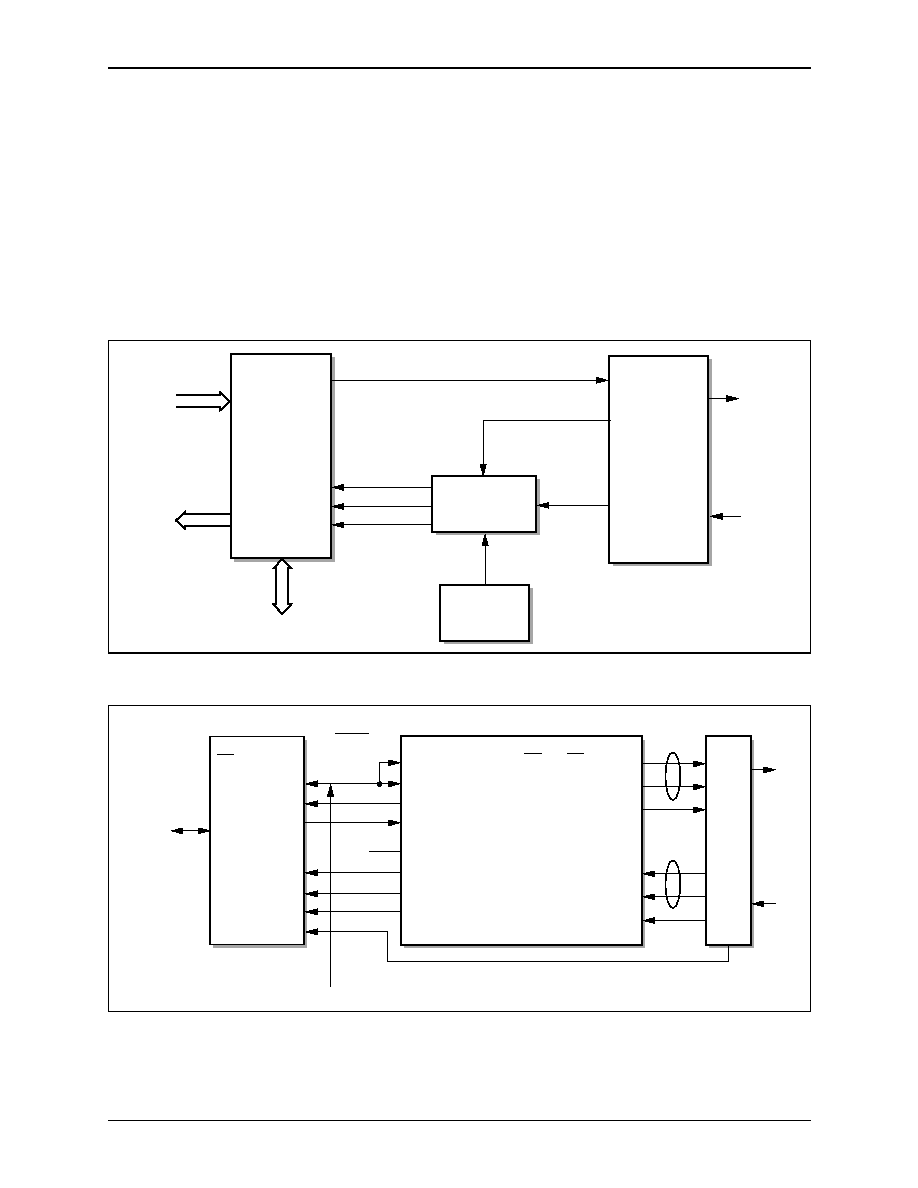
Figure 1-7. CN8223 Connected to Bt8360
Rx
RXIN[0]
TXOUT[3]
RXIN[4]
TXCKI
RXCKI
TXIN
RXIN[3]
CN8223
LIU
Tx
Tx Data
Rx Data
Derived
Cells
ATM
RCKO/SLCKI
RFSYO/SLFSYO
SLSYI
XBCKI
Pin
Pin
Pin
TXCKI
TXSYI
TXDATO
RXCKI
RXSYI
RXLOS*
Signal
30
32
36
10
18
15
19
43
27
30
37/49
38/41
36/55
50
29
63
62
61
7
6
8
RPOSI
RNEGI
RCKI
XPOSO
XNEGO
XCKO
XBSFSYO
XCKI
XPCMI
System Clock
Tx Clock
Layer
Bt8360
RXDATI
RPCMO/SLPCMO
8223_007
CN8223
1.0 Product Description
ATM Transmitter/Receiver with UTOPIA Interface
1.8 CN8223 Applications
100046C
Conexant
1-15
Figure 1-8
illustrates an example implementation of the CN8223 using a
Bt8510 External E1 Framer.
Figure 1-9
illustrates an example implementation of
the CN8223 using a Bt8370 External T1/E1 Framer.
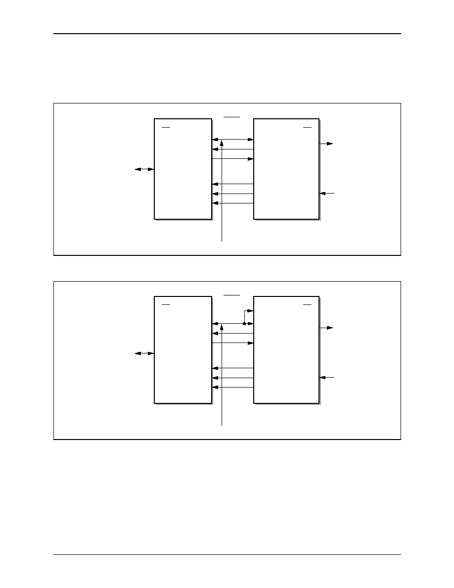
Figure 1-8. CN8223 Connected to Bt8510
Rx
RXIN[0]
TXOUT[3]
TXCKI
RXCKI
TXIN
RXIN[3]
CN8223
8223_008
Tx
Cells
ATM
RSYNCO
RPCMO
Pin
Pin
TXCKI
TXSYI
TXPATO
RXCKI
RXSYI
Signal
30
32
36
10
18
15
27
30
37
38
36
29
XSYNCO
XCKI
XPCMI
System Clock
Layer
RCKO
Bt8510
RXDATI
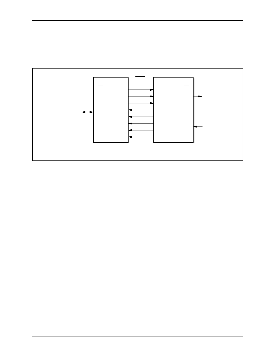
Figure 1-9. CN8223 Connected to Bt8370
Rx
RXIN[0]
TXOUT[3]
TXCKI
RXCKI
TXIN
RXIN[3]
CN8223
8223_009
Tx
Cells
ATM
RMSYNC
RPCMO
Pin
Pin
TXCKI
TXSYI
TXPATO
RXCKI
RXSYI
Signal
30
32
36
10
18
15
36
34
48
44
42
64
37
TMSYNC
TCKI
TSBCKI
TPCMI
System Clock
Layer
RCKO
Bt8370
RXDATI
1.0 Product Description
CN8223
1.8 CN8223 Applications
ATM Transmitter/Receiver with UTOPIA Interface
1-16
Conexant
100046C
Figure 1-10
illustrates an example implementation of the CN8223 using a
TDK 78P7200 T3 LIU. Unused pins on the CN8223 must be tied as follows:
unused RXIN_8:0 pins tie to ground, PECL inputs RXCKI_HS±, RXIN_HS±,
and TXCKI_HS± tie to +5 V.
1.8.1 CN8223 as a DS3 or E3 G.751 Framer without ATM Cell Delineation
The CN8223 can be used as a DS3 or an E3 G.751 framer with parallel input and
serial output by making the following changes:
∑
Set the configuration registers for transparent operation.
∑
Disable the parallel interface.
∑
Disable line loopback.
In this setup, the receive frame sync pulse is on pin 43, TXOUT[5]. Data is
received on pin 56, TXOUT[6]. The receive clock is derived from the LIU device.
Data is transmitted through the parallel UTOPIA interface.
Figure 1-10. CN8223 Connected to TDK 78P7200
Rx
RXIN[4]
TXCKI
TXOUT[1]
RXCKI
TCLKO
RXIN[2]
TXOUT[2]
RXIN[1]
CN8223
8223_010
Tx
Cells
ATM
RPOS
LOWSIG
Pin
Pin
Signal
31
35
34
10
17
16
19
30
14
23
24
25
27
15
27
TPOS
TNEG
TCLK
RCLK
System Clock
(44.736 MHz)
Layer
RNEG
TDK 78P7200

CN8223
1.0 Product Description
ATM Transmitter/Receiver with UTOPIA Interface
1.9 Logic Diagram
100046C
Conexant
1-17
1.9 Logic Diagram
The CN8223 is a single CMOS integrated circuit, packaged in a 160-pin Plastic
Quad Flat Pack (PQFP).
Figure 1-11
illustrates a CN8223 logic diagram. The line
framer/PHY interface consists of 33 pins. The framing overhead interface
consists of 22 pins. The FIFO interface consists of 18 data pins, 8 control inputs,
and 17 control outputs. The microprocessor interface consists of 8 clock and
control inputs, a 16-bit data bus, a 7-bit address bus, and 2 interrupt outputs.
Additionally, there are 11 power and 12 ground pins. Detailed pin descriptions are
given in
Table 1-2
.
Clock and control inputs consist of an external 8 kHz reference for the PLCP
at E3 and DS3 rates, a one-second input to synchronize status collection timing in
multiple-port applications, a "hold receiver" input that can externally disable cell
validation when an external framer loses frame or signal, three test inputs, and a
reset input. A one-second clock output is provided to allow synchronization of
status collection for multiple CN8223s or for CN8223s and framers. When a
single CN8223 is used, ONESECO should be connected to ONESECI. This
timing output is derived from the external 8 kHz reference clock input on 8KCKI.
An 8 kHz clock from the line receiver is available on RMRKR[1], pin 8.
NOTE:
RMRKR[1] is not available in DS-3 direct cell mapping mode.

1.0 Product Description
CN8223
1.9 Logic Diagram
ATM Transmitter/Receiver with UTOPIA Interface
1-18
Conexant
100046C
Figure 1-11. CN8223 Logic Diagram
Receive Clock Input
Receive Clock In PECL
Receive Serial In PECL
Receive Input
Transmit Clock Input
Transmit Clock In PECL
Transmit Input
Transmit Overhead
FIFO Data Bus In
FIFO Control Input
8 kHz Clock Input
One-Second Clock Sync
Receiver Hold Input
Test Input
Reset
Processor Clock
Chip Select
Address Strobe
Write/Read Control
Output Enable
Processor Data Bus
Address Bus
8/16-Bit Mode Select
Test Inputs
Bus In
98≠105,
108
109≠116
Microprocessor
Transmit Clock Output
Transmit Outputs
Transmit Clock Out PECL
Transmit Serial Out PECL
Loss of Cell Delineation
RXCKI
RXCKI_HS
±
RXIN_HS
±
RXIN[8:0]
TCLKO
TXOUT[8:0]
TCLKO_HS
±
TXOUT_HS
±
LOCD
Line Framer/PHY
Interface
I
I
I
I
TXOVH[7:0]
I
TXCKI
TXCKI_HS
±
TXIN
I
I
I
O
O
O
O
O
Framing Overhead
Interface
O
O
O
Receive Overhead Bus Out
Receive Overhead Markers
Receive Overhead Clocks
Transmit Overhead Clock
Transmit Overhead Marker
O
O
RXOVH[7:0]
RMRKR[1:0]
ROVH_CLK[1:0]
TOVH_CLK
TMRKR
FDAT_IN[8:0]
FCTRL_IN[7:0]
I
I
UTOPIA/FIFO
Interface
FDAT_OUT[8:0]
FCTRL_OUT[16:0]
O
O
FIFO Data Bus Out
FIFO Control Outputs
Interface
I
I
I
I
I
I/O
PRCLK
CS
~
AS
~
W/R
~
OE
~
D[15:0]
A[7:1]
I
DL_INT
STAT_INT
O
O
FEAC/HDLC Interrupt
Status/Counter Interrupt
8KCKI
ONESECI
RCV_HLD
NTEST
RESET
I
I
I
I
I
Clock and Control
O One-Second Output
ONESECO
15≠19,
154,155
22,25
10
11,12
20,21
30
31
33≠36,
42,43,
56≠58
28,29
38,39
122
156≠159
2≠5,
8,9
6,7
23,24
32
44≠51
I
37
SEL8BIT
97
96
94
95
92
65,
82≠84
85≠91
62
61
123
59
119
118
55
52
143≠145,
148≠153
124≠132,
135≠142
63
64
60
68≠79,
TEST1, TEST3
I
117,
I = Input, O = Output
8223_011

CN8223
1.0 Product Description
ATM Transmitter/Receiver with UTOPIA Interface
1.10 Pin Definitions
100046C
Conexant
1-19
1.10 Pin Definitions
Figure 1-12
is a pinout diagram for the 160-pin ATM Transmitter/Receiver.
Table 1-2
lists pin names and numbers. Generally, all unused input pins should be
connected to ground and unused outputs should be left unconnected. However, if
pins TXOVH_7 to TXOVH_0 or RXIN_8 to RXIN_0 are not used, they must be
tied to a logic low level. Some of the RXIN pins may be used depending on the
configuration. If PECL inputs, RXCKI_HS±, RXIN_HS±, or TXCKI_HS±, are
not used, they must be tied to +5 V power.
Figure 1-12. CN8223 Pinout Diagram
VCC
D[12]
D[11]
D[10]
D[9]
D[8]
D[7]
D[6]
D[5]
D[4]
D[3]
D[2]
D[1]
VCC
GND
D[0]
STAT_INT
DL_INT
8KCKI
ONESECI
ONESECO
NTEST
TXOUT[8]
TXOUT[7]
TXOUT[6]
TOVH_CLK
VCC
GND
TMRKR
TXOVH[7]
TXOVH[6]
TXOVH[5]
TXOVH[4]
TXOVH[3]
TXOVH[2]
TXOVH[1]
TXOVH[0]
TXOUT[5]
TXOUT[4]
GND
121
122
123
124
125
126
127
128
129
130
131
132
133
134
135
136
137
138
139
140
141
142
143
144
145
146
147
148
149
150
151
152
153
154
155
156
157
158
160
GND
LOCD
RCV_HLD
FCTRL_OUT[0]
FCTRL_OUT[1]
FCTRL_OUT[2]
FCTRL_OUT[3]
FCTRL_OUT[4]
FCTRL_OUT[5]
FCTRL_OUT[6]
FCTRL_OUT[7]
FCTRL_OUT[8]
GND
VCC
FCTRL_OUT[9]
FCTRL_OUT[11]
FCTRL_OUT[12]
FCTRL_OUT[13]
FCTRL_OUT[14]
FCTRL_OUT[15]
FCTRL_OUT[16]
FDAT_OUT[0]
FDAT_OUT[1]
FDAT_OUT[2]
GND
VCC
FDAT_OUT[3]
FDAT_OUT[4]
FDAT_OUT[5]
FDAT_OUT[6]
FDAT_OUT[7]
FDAT_OUT[8]
RXIN[7]
RXIN[8]
RXOVH[0]
RXOVH[1]
RXOVH[2]
RXOVH[3]
VCC
119
12
0
118
117
116
115
114
113
112
111
110
109
108
107
106
105
104
103
102
101
100
99
98
97
96
95
94
93
92
91
90
89
88
87
86
85
84
83
82
81
80
79
78
77
76
75
74
73
72
71
70
69
68
67
66
65
64
63
62
61
60
59
58
57
56
55
54
53
52
51
50
49
48
47
46
45
44
43
42
41
VCC
T
EST
3
RES
ET
T
EST
1
FC
T
R
L_IN
[7]
FC
T
R
L_IN
[6]
FC
T
R
L_IN
[5]
FC
T
R
L_IN
[4]
FC
T
R
L_IN
[3]
FC
T
R
L_IN
[2]
FC
T
R
L_IN
[1]
FC
T
R
L_IN
[0]
F
D
A
T
_I
N
[
8]
VCC
F
D
A
T
_I
N
[
7]
F
D
A
T
_I
N
[
6]
F
D
A
T
_I
N
[
5]
F
D
A
T
_I
N
[
4]
F
D
A
T
_I
N
[
3]
F
D
A
T
_I
N
[
2]
F
D
A
T
_I
N
[
1]
F
D
A
T
_I
N
[
0]
PRCL
K
CS*
W/R*
AS
*
GND
OE
*
A[
7
]
A[
6
]
A[
5
]
A[
4
]
A[
3
]
A[
2
]
A[
1
]
D
[
15]
D
[
14]
D
[
13]
GND
GND
1
2
3
4
5
6
7
8
9
10
11
12
13
14
15
16
17
18
19
20
21
22
23
24
25
26
27
28
29
30
31
32
33
34
35
36
37
38
39
40
ATM
Transmitter/Receiver
CN8223
FCTRL_OUT[10]
159
GND
RXO
VH[4
]
RXO
VH[5
]
RXO
VH[6
]
RXO
VH[7
]
R
O
V
H
_C
LK
[1]
R
O
V
H
_C
LK
[0]
RM
RKR[1
]
RM
RKR[0
]
RX
CKI
RXC
KI_
H
S
≠
GND
VC
C
RX
IN[0]
RX
IN[2]
RX
IN[3]
RX
I
N
_
H
S
≠
RX
IN[5]
TXC
KI
_
H
S
≠
T
X
CKI_
HS
+
RX
IN[6]
TC
LK
O
TX
I
N
TX
O
U
T[
0
]
TX
O
U
T[
1
]
TX
O
U
T[
2
]
TX
O
U
T[
3
]
S
E
L8B
IT
TX
O
U
T
_
H
S
+
TX
O
U
T_H
S
≠
VC
C
RX
IN[1]
GND
VC
C
TC
L
K
O
_
H
S
+
TC
LK
O_H
S
≠
TX
C
K
I
RXCKI_
HS
+
RX
IN[4]
RXIN_
HS
+
8223_012

1.0 Product Description
CN8223
1.10 Pin Definitions
ATM Transmitter/Receiver with UTOPIA Interface
1-20
Conexant
100046C
Table 1-2. Hardware Signal Definitions (1 of 5)
Pin Label
Signal Name
No.
Type
I/O
Definition
Li
ne
F
r
am
er
/
P
H
Y
In
t
e
r
f
ac
e
RXCKI
Receive Clock
Input
10
CMOS/TTL
I
Receive clock for all line rates except STS-3c,
STM-1, and E4.
RXCKI_HS≠
RXCKI_HS+
Receive Clock
Input
11
12
PECL
PECL
I
I
Differential PECL level for high-speed modes.
Receive clock for STS-3c, STM-1, and E4. Tie to
+5 V if not used.
RXIN_HS≠
RXIN_HS+
Receive Serial
Input
20
21
PECL
PECL
I
I
Differential PECL level for high-speed modes.
Serial data in for STS-3c, STM-1, and E4. Tie to
+5 V if not used.
RXIN[0]
RXIN[1]
RXIN[2]
RXIN[3]
RXIN[4]
RXIN[5]
RXIN[6]
RXIN[7]
RXIN[8]
Receive Input
15
16
17
18
19
22
25
154
155
CMOS/TTL
CMOS/TTL
CMOS/TTL
CMOS/TTL
CMOS/TTL
CMOS/TTL
CMOS/TTL
CMOS/TTL
CMOS/TTL
I
I
I
I
I
I
I
I
I
Receive parallel and TAXI mode data inputs. Tie
to a logic low level if not used.
TXCKI
Transmit Clock
Input
30
CMOS/TTL
I
Transmit clock for all modes except STS-3c,
STM-1, and E4.
TXCKI_HS≠
TXCKI_HS+
Transmit Clock
Input
23
24
PECL
PECL
I
I
Differential PECL level for high-speed modes.
Transmit clock for STS-3c, STM-1, and E4. Tie to
+5 V if not used.
TXIN
Transmit Inputs
32
CMOS/TTL
I
Transmit serial data input for all modes except
STS-3c, STM-1, and E4.
TCLKO
Transmit Clock
Output
31
CMOS/TTL
O
Transmit clock output for all modes except
STS-3c, STM-1, and E4.
TXOUT[0]
TXOUT[1]
TXOUT[2]
TXOUT[3]
TXOUT[4]
TXOUT[5]
TXOUT[6]
TXOUT[7]
TXOUT[8]
Transmit Output
33
34
35
36
42
43
56
57
58
CMOS/TTL
CMOS/TTL
CMOS/TTL
CMOS/TTL
CMOS/TTL
CMOS/TTL
CMOS/TTL
CMOS/TTL
CMOS/TTL
O
O
O
O
O
O
O
O
O
Transmit parallel and TAXI mode data outputs.
TCLKO_HS+
TCLKO_HS≠
Transmit Clock Out
28
29
PECL
PECL
O
O
Differential PECL level. Transmit clock output for
STS-3c, STM-1, and E4.
TXOUT_HS+
TXOUT_HS≠
Transmit Serial Out
38
39
PECL
PECL
O
O
Differential PECL level. Transmit serial data
output for STS-3c, STM-1, and E4.
LOCD
Loss of Cell
Delineation
122
CMOS/TTL
O
Asserted when cell synchronization is lost.

CN8223
1.0 Product Description
ATM Transmitter/Receiver with UTOPIA Interface
1.10 Pin Definitions
100046C
Conexant
1-21
Fr
a
m
i
n
g
Ov
er
he
ad
In
t
e
r
f
ac
e
TXOVH[0]
TXOVH[1]
TXOVH[2]
TXOVH[3]
TXOVH[4]
TXOVH[5]
TXOVH[6]
TXOVH[7]
Transmit Overhead
Bus
44
45
46
47
48
49
50
51
CMOS/TTL
CMOS/TTL
CMOS/TTL
CMOS/TTL
CMOS/TTL
CMOS/TTL
CMOS/TTL
CMOS/TTL
I
I
I
I
I
I
I
I
Transmit bus input for
STS-1/STS-3c/STM-1/G.832 overhead. Tie to a
logic low level if not used.
RXOVH[0]
RXOVH[1]
RXOVH[2]
RXOVH[3]
RXOVH[4]
RXOVH[5]
RXOVH[6]
RXOVH[7]
Receive Overhead
Bus
156
157
158
159
2
3
4
5
CMOS/TTL
CMOS/TTL
CMOS/TTL
CMOS/TTL
CMOS/TTL
CMOS/TTL
CMOS/TTL
CMOS/TTL
O
O
O
O
O
O
O
O
Receive bus output for
STS-1/STS-3c/STM-1/G.832 overhead.
RMRKR[1]
RMRKR[0]
Receive Overhead
Markers
8
9
CMOS/TTL
CMOS/TTL
O
O
Used for overhead bus output. RMRKR[1] is an
8 kHz output synchronized to the received PLCP
frame. RMRKR[1] is not available in DS-3 direct
cell mapping mode.
ROVH_CLK[1]
ROVH_CLK[0]
Receive Overhead
Clocks
6
7
CMOS/TTL
CMOS/TTL
O
O
Used for overhead bus output.
TOVH_CLK
Transmit Overhead
Clock
55
CMOS/TTL
O
Used for bus input.
TMRKR
Transmit Overhead
Marker
52
CMOS/TTL
O
Used for bus input in modes 4, 5, 6 and 7 (OC3,
OC1, E4 and G.832 E3).
Table 1-2. Hardware Signal Definitions (2 of 5)
Pin Label
Signal Name
No.
Type
I/O
Definition

1.0 Product Description
CN8223
1.10 Pin Definitions
ATM Transmitter/Receiver with UTOPIA Interface
1-22
Conexant
100046C
UTO
P
IA
/FIF
O Inte
rfa
c
e
FDAT_IN[0]
FDAT_IN[1]
FDAT_IN[2]
FDAT_IN[3]
FDAT_IN[4]
FDAT_IN[5]
FDAT_IN[6]
FDAT_IN[7]
FDAT_IN[8]
FIFO Data Bus
98
99
100
101
102
103
104
105
108
CMOS/TTL
CMOS/TTL
CMOS/TTL
CMOS/TTL
CMOS/TTL
CMOS/TTL
CMOS/TTL
CMOS/TTL
CMOS/TTL
I
I
I
I
I
I
I
I
I
FIFO interface input data bus for transmit. See
Section 2.7.1
.
FCTRL_IN[0]
FCTRL_IN[1]
FCTRL_IN[2]
FCTRL_IN[3]
FCTRL_IN[4]
FCTRL_IN[5]
FCTRL_IN[6]
FCTRL_IN[7]
FIFO Control Input
109
110
111
112
113
114
115
116
CMOS/TTL
CMOS/TTL
CMOS/TTL
CMOS/TTL
CMOS/TTL
CMOS/TTL
CMOS/TTL
CMOS/TTL
I
I
I
I
I
I
I
I
FIFO interface empty/full flag inputs. See
Section 2.7.1
.
FDAT_OUT[0]
FDAT_OUT[1]
FDAT_OUT[2]
FDAT_OUT[3]
FDAT_OUT[4]
FDAT_OUT[5]
FDAT_OUT[6]
FDAT_OUT[7]
FDAT_OUT[8]
FIFO Data Bus Out
143
144
145
148
149
150
151
152
153
CMOS/TTL
CMOS/TTL
CMOS/TTL
CMOS/TTL
CMOS/TTL
CMOS/TTL
CMOS/TTL
CMOS/TTL
CMOS/TTL
O
O
O
O
O
O
O
O
O
FIFO interface output data bus for receive. See
Section 2.7.1
.
FCTRL_OUT[0]
FCTRL_OUT[1]
FCTRL_OUT[2]
FCTRL_OUT[3]
FCTRL_OUT[4]
FCTRL_OUT[5]
FCTRL_OUT[6]
FCTRL_OUT[7]
FCTRL_OUT[8]
FCTRL_OUT[9]
FCTRL_OUT[10]
FCTRL_OUT[11]
FCTRL_OUT[12]
FCTRL_OUT[13]
FCTRL_OUT[14]
FCTRL_OUT[15]
FCTRL_OUT[16]
FIFO Control
Outputs
124
125
126
127
128
129
130
131
132
135
136
137
138
139
140
141
142
CMOS/TTL
CMOS/TTL
CMOS/TTL
CMOS/TTL
CMOS/TTL
CMOS/TTL
CMOS/TTL
CMOS/TTL
CMOS/TTL
CMOS/TTL
CMOS/TTL
CMOS/TTL
CMOS/TTL
CMOS/TTL
CMOS/TTL
CMOS/TTL
CMOS/TTL
O
O
O
O
O
O
O
O
O
O
O
O
O
O
O
O
O
FIFO interface strobe and control outputs. See
Section 2.7.1
.
Table 1-2. Hardware Signal Definitions (3 of 5)
Pin Label
Signal Name
No.
Type
I/O
Definition

CN8223
1.0 Product Description
ATM Transmitter/Receiver with UTOPIA Interface
1.10 Pin Definitions
100046C
Conexant
1-23
Mi
cr
o
p
r
oc
es
s
o
r
In
ter
f
ac
e
SEL8BIT
8/16 Bit Mode
Select
37
CMOS/TTL
I
If asserted, this pin selects an 8-bit
microprocessor bus. If not asserted, it selects a
16-bit bus.
PRCLK
Processor Clock
97
CMOS/TTL
I
Clock input to the microprocessor interface. All
inputs are synchronous to this clock except OE~.
All read and write operations require two cycles
of PRCLK. PRCLK must run continuously at a
minimum frequency of 2 times the cell rate.
CS~
Chip Select
96
CMOS/TTL
I
Must be logic low to address chip. Must be low
to enable a read or write operation and should
be stable throughout the cycle.
AS~
Address Strobe
94
CMOS/TTL
I
If this pin is low, a new address is loaded on the
rising edge of PRCLK for the operation in the
following clock period. If this pin is high and
CS~ is low, a read or a write operation is
executed. The address strobe can stay low for
multiple clock periods. Address strobe cannot
stay high with CS~ low for multiple clock
periods.
W/R~
Write/Read Control
95
CMOS/TTL
I
If this pin is low when CS~ is low, the following
cycle is a read operation. If this signal is high
when CS~ is low, the data presented at the end
of the following clock cycle will be written if CS~
is still low on that cycle.
OE~
Output Enable
92
CMOS/TTL
I
This signal must be low to enable the data
output for a read cycle. Data bus outputs are
three-stated if this signal is high. The data is
valid between clock edges on a read cycle when
this pin is low. This pin may be connected
directly to ground, if desired.
DL_INT
FEAC/HDLC
Interrupt
63
CMOS/TTL
O
Active-low data link channel interrupt output
with open drain.
STAT_INT
Status/Counter
Interrupt
64
CMOS/TTL
O
Active-low status/counter interrupt with open
drain.
D[0]
D[1]
D[2]
D[3]
D[4]
D[5]
D[6]
D[7]
D[8]
D[9]
D[10]
D[11]
D[12]
D[13]
D[14]
D[15]
Processor Data
Bus
65
68
69
70
71
72
73
74
75
76
77
78
79
82
83
84
CMOS/TTL
CMOS/TTL
CMOS/TTL
CMOS/TTL
CMOS/TTL
CMOS/TTL
CMOS/TTL
CMOS/TTL
CMOS/TTL
CMOS/TTL
CMOS/TTL
CMOS/TTL
CMOS/TTL
CMOS/TTL
CMOS/TTL
CMOS/TTL
I/O
I/O
I/O
I/O
I/O
I/O
I/O
I/O
I/O
I/O
I/O
I/O
I/O
I/O
I/O
I/O
This signal is a 16-bit bidirectional data bus for
read and write data.
Table 1-2. Hardware Signal Definitions (4 of 5)
Pin Label
Signal Name
No.
Type
I/O
Definition

1.0 Product Description
CN8223
1.10 Pin Definitions
ATM Transmitter/Receiver with UTOPIA Interface
1-24
Conexant
100046C
Mi
crop
roce
sso
r I
n
t
e
rf
ace
A[1]
A[2]
A[3]
A[4]
A[5]
A[6]
A[7]
Address Bus
85
86
87
88
89
90
91
CMOS/TTL
CMOS/TTL
CMOS/TTL
CMOS/TTL
CMOS/TTL
CMOS/TTL
CMOS/TTL
I
I
I
I
I
I
I
Seven-bit address input for addressing registers
within the chip. Addresses are loaded when AS~
is low.
Clo
c
k an
d Co
ntr
o
l
8KCKI
8 kHz Reference
Clock Input
62
CMOS/TTL
I
Used to synchronize PLCP, and drive ONESECO.
ONESECI
One-Second Clock
Sync
61
CMOS/TTL
I
1 Hz input used to latch line status every one
second.
RCV_HLD
Receiver Hold
Input
123
CMOS/TTL
I
If asserted, this pin stops the cell receiver.
NTEST
Test Input
59
CMOS/TTL
I
Connect to Vcc for normal operation.
TEST1
TEST3
Test Inputs
117
119
CMOS/TTL
CMOS/TTL
I
I
Connect to ground for normal operation.
RESET
Reset
118
CMOS/TTL
I
Active-high pulse on power-up for at least
100 ns. This pin resets the internal state
machines. It does not affect the contents of the
registers, except bit 9 of register 0x02.
ONESECO
One-Second
Output
60
CMOS/TTL
O
One-second count derived from count of 8 kHz
input.
Su
pp
ly
V
o
l
t
ag
e
VCC
Supply Voltage
14
27
40
54
67
80
107
120
134
147
160
CMOS/TTL
CMOS/TTL
CMOS/TTL
CMOS/TTL
CMOS/TTL
CMOS/TTL
CMOS/TTL
CMOS/TTL
CMOS/TTL
CMOS/TTL
CMOS/TTL
--
--
--
--
--
--
--
--
--
--
--
Eleven pins are provided for supply voltage.
GND
Ground
1
13
26
41
53
66
81
93
106
121
133
146
CMOS/TTL
CMOS/TTL
CMOS/TTL
CMOS/TTL
CMOS/TTL
CMOS/TTL
CMOS/TTL
CMOS/TTL
CMOS/TTL
CMOS/TTL
CMOS/TTL
CMOS/TTL
--
--
--
--
--
--
--
--
--
--
--
--
Twelve pins are provided for ground.
Table 1-2. Hardware Signal Definitions (5 of 5)
Pin Label
Signal Name
No.
Type
I/O
Definition

100046C
Conexant
2-1
2
2.0 Functional Description
This chapter describes the CN8223 architecture and functional blocks.
Figure 2-1
and
Figure 2-2
illustrates detailed signal paths of the receiver and transmitter.
Figure 2-1. CN8223 Receiver Block Diagram
STS-1/
STS-3c/
G.832
STM-1
Serial/Parallel
DS-3/G.751
E3 Framer
STS-1/
STS-3c/
STM-1
G.832
Framer
Serial
Bipolar
Data
Serial
NRZ
Data
Enable
B3ZS/HDB3
MUX
Serial/
Parallel
External
Framer
Mode
Clock, Sync, Serial Data
Octets
MUX
Parallel Input
Octet, Clock
100 Mbps
TAXI Interface
PHY
Mode
PLCP
Framer
HEC
Align.
Framer
MUX
ATM
Cell
Receiver
Alignment
Mode
Overhead Output
MUX
8223_013
Figure 2-2. CN8223 Transmitter Block Diagram
MUX
STS-1/
STS-3c/
STM-1
G.832
Gen.
Overhead Input
PLCP
Gen.
ATM
Cell
Gen.
DS3/
G.751 E3
Gen.
B3ZS/
HDB3
Encode
MUX
Serial/
Parallel
Data Out
8223_014

2.0 Functional Description
CN8223
2.1 Microprocessor Interface
ATM Transmitter/Receiver with UTOPIA Interface
2-2
Conexant
100046C
2.1 Microprocessor Interface
All control and status functions are provided via a direct microprocessor
interface. Address maps for the microprocessor are given in
Chapter 3.0
. There
are two types of address spaces:
∑
Read and write control registers
∑
Read-only status registers and counters
Write operations are fully decoded. Write operations to undefined addresses have
no effect. Read operations from undefined addresses have undefined results.
The microprocessor interface to the CN8223 consists of 31 pins (detailed in
Table 1-2
). The CN8223 connects to the microprocessor as if it were clocked
RAM memory. For timing diagram details, see
Section 4.3.1
.
2.1.1 8/16-Bit Interface
The CN8223 supports an 8-bit or 16-bit microprocessor interface. To select the
8-bit data bus, connect the SEL8BIT pin to VCC. This configures all control and
status registers in the part for byte-wide operation. Byte addressing is
accomplished by using the D15 pin as the byte high/low select. When D15 is low,
the low byte of the addressed register is read or written, and the high byte is
unaffected. When D15 is high, the high byte of the addressed register is read or
written, and the low byte is unaffected. When reading register locations, the high
byte of the addressed location is internally latched so that it can be read in the
next operation. Therefore, the low byte of a word address should be read first,
then the high byte, to prevent loss of data. When SEL8BIT is low, the interface is
configured with a 16-bit bus.
2.1.2 Interrupts
The CN8223 is designed for an interrupt-driven environment. After initialization,
status events, error events, and counter overflows generate interrupts that run
appropriate interrupt service routines.
Two active-low interrupt pins are provided for the microprocessor interface.
STAT_INT provides interrupts for all status and error conditions. DL_INT
provides interrupts for the Far End Alarm Control (FEAC) channel contained in
the internal DS3 framer and for the internal High-Level Data Link Control
(HDLC) formatter used for various data links. Both interrupt pins are configured
as open drain to facilitate external wire-OR connections.
Each interrupt source has a bit in an interrupt enable register and in an
interrupt status register. This allows the microprocessor to control which
conditions cause interrupts and to determine the source of the interrupt. The
status registers are described in
Chapter 3.0
.
NOTE:
Receiver interrupts will not function if the receive clock is not active. For
example, if losing the signal to the line interface causes the receive clock
recovery circuit to be disabled, the CN8223 will not respond to an LOS
interrupt.

CN8223
2.0 Functional Description
ATM Transmitter/Receiver with UTOPIA Interface
2.2 Line Framers
100046C
Conexant
2-3
2.2 Line Framers
This section describes the operation and control of the internal framers for DS3,
E3 (both G.751 and G.832), E4 (G.832), STS-1, and STS-3c/STM-1 formatted
serial streams. The transmit and receive serial interfaces can operate at up to
155 MHz. Detailed timing information for the line interface is given in
Chapter 4.0
.
The framer receive circuitry recovers the frame location from the serial stream
and provides cell octets to the HEC/PLCP cell alignment block. All alarm and
error conditions are monitored and reported in status registers and event counters.
The framer transmit circuitry receives cell octets from the HEC/PLCP cell
alignment block and adds line framing overhead information. All alarm and error
conditions can be generated from control registers.
External interfaces to this block and the interface to the rest of the CN8223 are
illustrated in
Table 1-2
. The CN8223 line mode is set for both transmit and
receive in the CONFIG_1 register [0x00].
Table 2-1
lists the valid line modes set
by CONFIG_1.
Table 2-1. Valid CONFIG_1 Line Mode Settings, Bits 7≠0
Type of Line Input Signal
PHY
Type
Unframed
Input
Disable
B3ZS/
HDB3
External
Framer
Enable
Parallel
Interface
Enable
HEC
Align
DS1
0
0
0
1
0
0 or 1
DS1 (externally gapped 192 bits/frame)
0
1
0
1
0
0
E1
1
0
0
1
0
0 or 1
E1 (externally gapped TS0 and TS16)
1
1
0
1
0
0
DS3, internal framer
2
0
0 or 1
0
0
0 or 1
DS3, external framer
2
0
0
1
0
0 or 1
DS3, external framer (gapped 84/85 bits)
2
1
0
1
0
0
E3, internal G.751 format
3
0
0 or 1
0
0
0
E3, external G.751 format
3
0
0
1
0
0
E3, external G.751 format (gapped first 16
bits)
3
1
0
1
0
0
E3, internal G.832 format
4
x
0 or 1
0
0
1
E4, internal G.832 format
5
x
1
0
0
1
STS-1, internal framer
6
x
0 or 1
0
0
1
STS-3c/STM-1, internal framer
7
x
1
0
0
1
Parallel or TAXI interface, 53 octet cells
0
x
0
1
1
1
NOTE(S):
x = Don't Care.

2.0 Functional Description
CN8223
2.2 Line Framers
ATM Transmitter/Receiver with UTOPIA Interface
2-4
Conexant
100046C
2.2.1 Internally Framed Transmit Line Interface
In internal framer mode, the transmitter provides positive and negative pulse
indications and a transmit output clock to an external Line Interface Unit (LIU)
(or output clock and NRZ serial data if internal B3ZS/HDB3 encoding is
disabled) in response to a transmit input clock.
Table 2-2
gives the internal framing mode interface connections. The
functional timing for the transmit line interface is similar for all internal framer
modes.
Figure 2-3
illustrates the interface timing when the internal B3ZS/HDB3
encoder is enabled. The TCLKO phase shown can be inverted with Invert TX
Clock Output [bit 7] of the CONFIG_3 register [0x02].
Table 2-2. Internal Framer Transmitter Interface Connections
Signal Name
Connect to CN8223 Pin
Transmit Clock Input (TXCKI)
TXCKI
Transmit Clock Output (TCLKO)
TCLKO
Transmit Positive Data (TXPOS)
TXOUT[1]
Transmit Negative Data (TXNEG)
TXOUT[2]
Figure 2-3. Internal Framer Transmitter Interface Timing with Line Encoding
TCLKO
TXPOS
TXNEG
8223_015
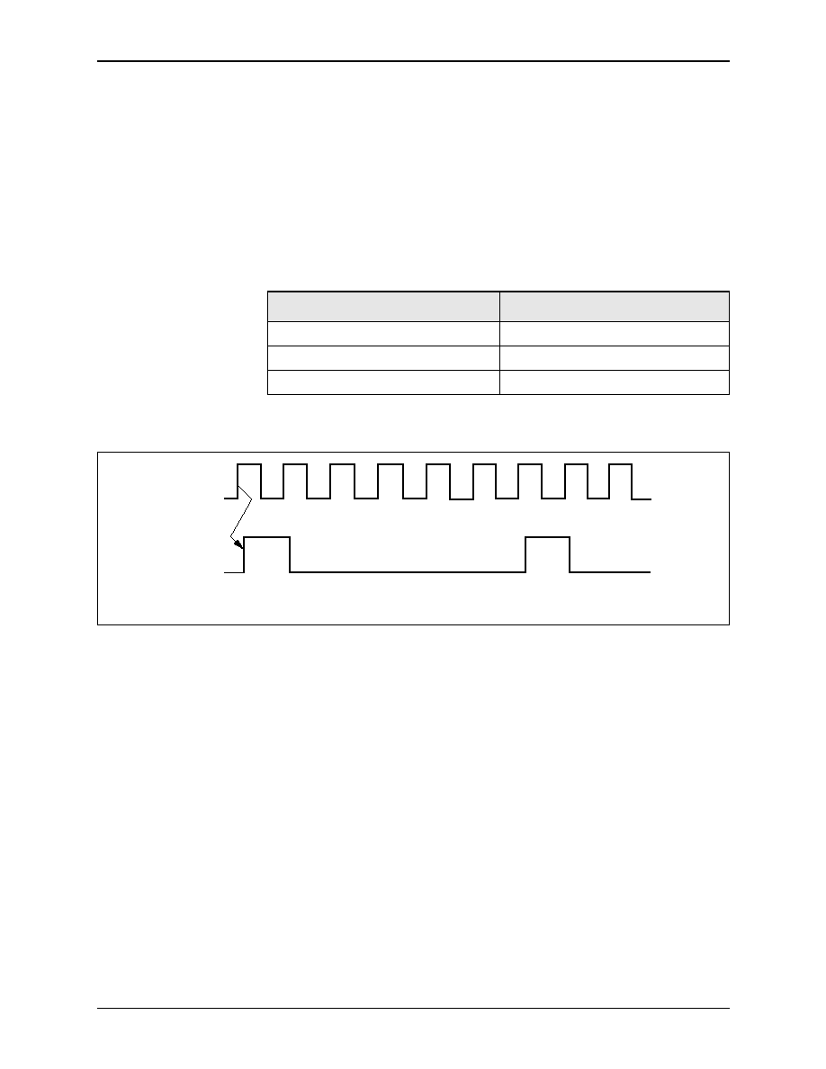
CN8223
2.0 Functional Description
ATM Transmitter/Receiver with UTOPIA Interface
2.2 Line Framers
100046C
Conexant
2-5
2.2.1.1 High-Speed
PECL Transmit Interface
For STS-3c, STM-1, or E4, the high-speed PECL interface is used. This mode is
used in any case where an external LIU/decoder is used (such as E4 and
STS-3c/STM-1 CMI decoding). If the mode is set to E4 or STS-3c/STM-1 in
CONFIG_1, then the outputs are taken from the "HS±" versions of the output
pins. The TCLKO (and TCLKO_HS±) phase shown can be inverted with the
Invert TX Clock Output control bit.
Table 2-3
lists the interface connections for the internal framing mode without
line encoding.
Figure 2-4
illustrates the interface timing when the internal
B3ZS/HDB3 encoder is disabled.
Table 2-3. Internal Framing Unencoded Transmitter Connections (STS-3c, STM-1, E4)
Signal Name
Connect to CN8223 Pin
Transmit Clock Input (TXCKI)
TXCKI_HS±
Transmit Data (TXDATO)
TXOUT_HS±
Transmit Clock Output (TCLKO)
TCLKO_HS±
Figure 2-4. Internal Framer Transmitter Interface Timing Without Line Encoding
TCLKO
TXDATO
8223_016

2.0 Functional Description
CN8223
2.2 Line Framers
ATM Transmitter/Receiver with UTOPIA Interface
2-6
Conexant
100046C
2.2.2 Internally Framed Receive Line Interface
In internal framer mode, the receiver inputs are positive and negative pulse
indications, and the receive clock (and NRZ serial data if internal B3ZS/HDB3
decoding is disabled) comes from an external LIU.
Table 2-4
lists the interface connections for all of the internal framing modes.
The functional timing for the receive line interface is similar for all internal
framer modes.
Figure 2-5
illustrates the interface timing when the internal
B3ZS/HDB3 decoder is enabled. The RXPOS and RXNEG inputs are sampled on
the falling edge of the RXCKI clock input. Data inputs can be sampled on the
rising edge of the input clock by setting Invert RX Clock Sampling [bit 8] in
register CONFIG_3 [0x02].
Table 2-4. Internal Framer Receiver Interface Connections
Signal Name
Connect to CN8223 Pin
Receive Clock Input (RXCKI)
RXCKI
Receive Positive Data (RXPOS)
RXIN[1]
Receive Negative Data (RXNEG)
RXIN[2]
Receive Loss of Signal (RXLOS~~)
RXIN[4]
Figure 2-5. Internal Framer Receiver Interface Timing
RXCKI
RXPOS
RXNEG
8223_017
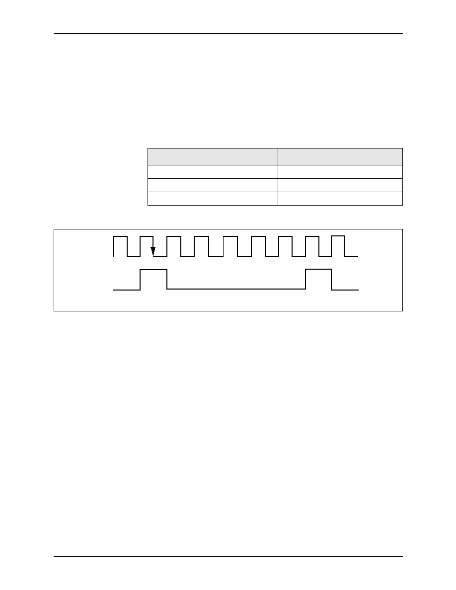
CN8223
2.0 Functional Description
ATM Transmitter/Receiver with UTOPIA Interface
2.2 Line Framers
100046C
Conexant
2-7
2.2.2.1 High-Speed
PECL Receive Interface
STS-3c, STM-1 and E4 use the high-speed PECL interface. This mode is used in
any case where an external LIU/decoder is used (such as E4 and STS-3c/STM-1
CMI decoding). If the mode is set to E4 or STS-3c/STM-1 in CONFIG_1, then
the inputs are taken from the "HS
±
" versions of the input pins. RXDATI input is
sampled on the falling edge of RXCKI. RXDATI can be sampled on the rising
edge of the input clock by setting the Invert RX Clock Sampling bit.
Table 2-5
lists the connections for internal framer Rx with the encoder disabled;
Figure 2-6
illustrates the timing with the coder disabled.
2.2.2.2 Receiver
Framing Operation
Five modes are provided for receiver framing operation: DS3, G.751 E3, G.832
E3/E4, STS-1, and STS-3c/STM-1.
In DS3 mode, a parallel-search framing circuit recovers the subframe and
M-frame alignments in the DS3 signal. Framing is initiated by an out-of-frame
condition as determined by the receiver frame bit-check circuitry. When 3 out of
16 consecutive subframing (F) bits are in error or when 2 out of 3 consecutive
M-frames have M bit errors, an out-of-frame condition is declared.
In G.751 E3 mode, a serial search for the 10-bit FAS pattern (1111 0100 00) is
conducted. When three consecutive correct patterns are found, the receiver is
declared to be in frame. An out-of-frame condition is declared when four
consecutive incorrect FAS patterns are detected.
In G.804 E3/E4 and STS-1/STS-3c/STM-1 modes, an octet alignment by the
serial-to-parallel conversion circuit is found in conjunction with an octet search
for the SONET A1/A2 framing pattern (which is the same pattern as, but not
related to, the PLCP A1/A2 bytes). When two consecutive good patterns are
found, the receiver is declared to be in frame. An out-of-frame (OOF) condition is
declared when four consecutive incorrect A1/A2 patterns are detected.
In STS-3c/STM-1 mode, an octet alignment by the serial-to-parallel
conversion circuit is found in conjunction with an octet search for the third A1
and the first A2 octets.
In STS-1 Mode, if STS-1 Stuffing Option [bit 15] in CONFIG_1 [0x00] is set,
then columns 30 and 59 in the payload envelope are stuff columns, and these
octets will not be interpreted as ATM cell octets. If this bit is not set, then all 86
columns of the SPE will be interpreted as ATM cell octets.
Table 2-5. Connections for Internal Framer Rx, Encoder Disabled (STS-3c, STM-1, E4)
Signal Name
Connect to CN8223 Pin
Receive Clock Input (RXCKI)
RXCKI or RXCKI_HS±
Receive Data (RXDATI)
RXIN[0] or RXIN_HS±
Receive Loss of Signal (RXLOS~)
RXIN[4]
Figure 2-6. Timing for Internal Framer Receiver, Encoder Disabled
RXCKI
RXDATI
8223_018

2.0 Functional Description
CN8223
2.2 Line Framers
ATM Transmitter/Receiver with UTOPIA Interface
2-8
Conexant
100046C
2.2.3 Externally Framed Transmit Line Interface
In external framer mode, the transmitter inputs are a clock and a synchronization
signal that indicate the position of framing bits in the DS1, E1, DS3, or E3
framing signal. The transmit data stream output is a single serial output. The
synchronization signal period can be any multiple of the frame period.
Functional timing for the transmit line interface is similar for all external
framer modes. These interfaces are compatible with Conexant framers Bt8360 for
DS1, Bt8510 for E1, Bt8370 for E1/T1, and Bt8330B for DS3 and E3. Interface
connections for these serial, external framing modes are given in
Table 2-6
.
Figure 2-7
illustrates the transmit timing for the DS1 interface. TXCKI is
1.544 MHz. TXSYI has a rising edge prior to the sampling of the frame bit. This
signal does not have to be present at every frame; in particular, it can be a
superframe synchronization signal with a period of 3 ms. TXDATO is the output
signal; it transitions in response to the rising edge of TXCKI and can be sampled
on the following falling edge. The framing bit position content in the output
stream is undefined.
Table 2-6. Serial External Framer Transmitter Interface Connection
Signal Name
Connect to CN8223 Pin
Transmit Clock Input (TXCKI)
TXCKI
Transmit Sync Input (TXSYI)
TXIN
Transmit Data Output (TXDATO)
TXOUT[3]
Figure 2-7. DS1 Interface Transmit Timing
7
8
S
2
3
4
5
6
7
8
F
S
2
3
4
5
6
7
Channel 24
Channel 1
TXCKI
TXSYI
TXDATO
8223_019
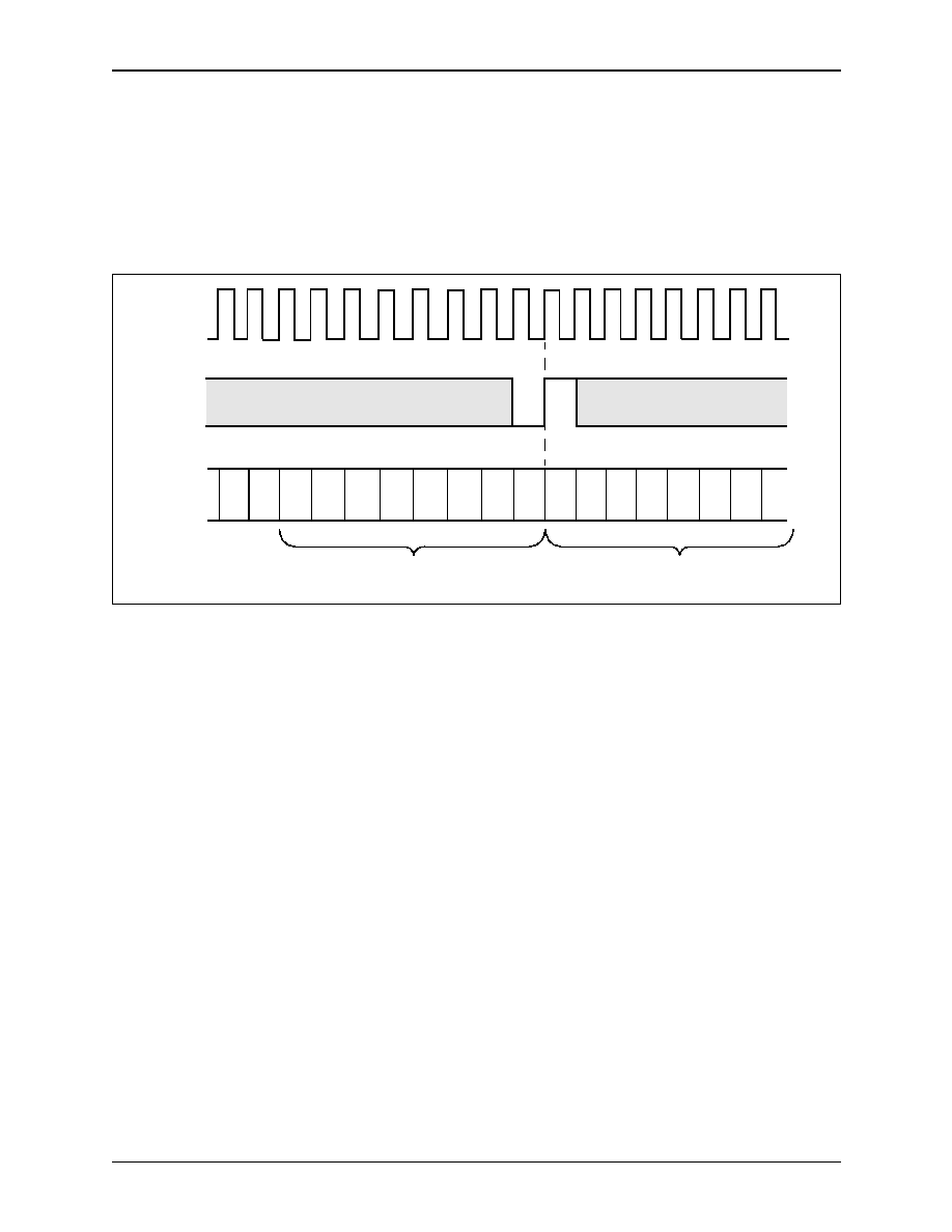
CN8223
2.0 Functional Description
ATM Transmitter/Receiver with UTOPIA Interface
2.2 Line Framers
100046C
Conexant
2-9
Figure 2-8
illustrates the transmit timing for the E1 interface. TXCKI is
2.048 MHz. TXSYI has a rising edge prior to the sampling of the first bit of time
slot 0. This signal can be present every 2 ms. TXDATO is the output signal; it
transitions in response to the rising edge of TXCKI, and can be sampled on the
following falling edge. The content of time slot 0 and time slot 16 of the output is
undefined.
Figure 2-8. E1 Interface Transmit Timing
Time Slot 31
TXCKI
TXSYI
TXDATO
7
8
S
2
3
4
5
6
7
8
1
2
3
4
5
6
7
8
Time Slot 0
8223_020

2.0 Functional Description
CN8223
2.2 Line Framers
ATM Transmitter/Receiver with UTOPIA Interface
2-10
Conexant
100046C
Figure 2-9
illustrates the transmit timing for the DS3 interface. TXCKI has a
frequency of 44.736 MHz. TXSYI (active low) is sampled on falling clock
transitions, and TXDATO changes on falling clock edges. TXSYI has a rising
edge after the sampling of the overhead bit (once every 85 bits). TXDATO is the
output signal; it transitions in response to the falling edge of TXCKI, and can be
sampled on the following falling edge. This timing is compatible with the
Conexant Bt8330B DS3/E3 framer, using the TXOVH output of that circuit to
synchronize the CN8223 input. The content of the frame bit position is
undefined.
Figure 2-9. DS3 Interface Transmit Timing
Information Field
TXCKI
TXSYI
TXDATO
X
Frame Bit Position
Information Field
8223_021

CN8223
2.0 Functional Description
ATM Transmitter/Receiver with UTOPIA Interface
2.2 Line Framers
100046C
Conexant
2-11
Figure 2-10
illustrates the transmit timing for the E3 interface. TXCKI has a
frequency of 34.368 MHz. TXSYI has a rising edge after the sampling of the last
bit of the frame alignment signal. TXDATO is the output signal; it transitions in
response to the falling edge of TXCKI, and can be sampled on the following
falling edge. This timing is compatible with the Conexant Bt8330B DS3/E3
framer using the TXOVH output. The frame alignment signal position is filled
with the value 0xCCCC. This value provides the four overhead bits (required by
ETSI prETS 300 214) that follow the frame alignment signal defined by ITU
G.751.
2.2.4 Externally Framed Receive Line Interface
The CN8223 external receive line interface has three inputs: clock, data, and
frame sync. Frame sync can be a multiple of the frame period.
Table 2-7
lists the
receiver connections for all external framing modes. The receive line inputs
consist of the receive clock (RXCKI), the receive sync input (RXSYI), and the
receive data input (RXDATI) when the external framer mode is selected.
Figure 2-10. E3 Interface Transmit Timing
Frame Alignment Signal Position
TXCKI
TXSYI
TXDATO
X
1
1
0
0
Information Field
X
X
X
X
X
X
X
X
X
8223_022
Table 2-7. External Framing Mode Receiver Connections
Signal Name
Connect to CN8223 Pin
Receive Clock Input (RXCKI)
RXCKI
Receive Sync Input (RXSYI)
RXIN[3]
Receive Data Input (RXDATI)
RXIN[0]
Receive Loss of Signal (RXLOS~)
RXIN[4]

2.0 Functional Description
CN8223
2.2 Line Framers
ATM Transmitter/Receiver with UTOPIA Interface
2-12
Conexant
100046C
The input timings are all similar: RXDATI and RXSYI are sampled on the
falling edge of the input clock; and the low-to-high transition of the sync signal
occurs during the interval of the frame bit for DS1 and DS3, with the first bit of
time slot 0 for E1, and the first bit of the frame-alignment signal for E3. For
brevity, only the DS1 timing is illustrated (
Figure 2-11
). The timing on this
interface is similar to the timing on the transmit interface. It is compatible with
Conexant framers. The data and sync inputs can be sampled on the rising edge of
the input clock by setting Invert RX Clock Sampling [bit 8] of CONFIG_3
[0x02].
In all framed, serial line formats, the content of the framing bit positions is
ignored. RXSYI does not need to be present every frame; it can be applied at any
submultiple of the frame rate (e.g., once every ESF superframe for DS1).
Figure 2-11. Receiver DS1 Line Interface Timing
Channel 24
RXCKI
RXSYI
RXDATI
8
7
Channel 1
6
5
4
3
2
S
7
6
5
4
3
2
S
F
8
7
8223_023

CN8223
2.0 Functional Description
ATM Transmitter/Receiver with UTOPIA Interface
2.3 Overhead Generation
100046C
Conexant
2-13
2.3 Overhead Generation
The CN8223 automatically receives and generates line overhead. For additional
flexibility, line overhead can be monitored and inserted for STS-3c, STM-1, and
G.832 E3/E4 modes.
2.3.1 Internal DS3 Mode
The transmitter circuitry automatically generates all F and M framing bits. The
transmitter calculates the parity of each M-frame and inserts this data into bits P1
and P2 of the following M-frame. Bits X1 and X2 contain 1s unless Transmit
Alarm Control [bit 6] of CONFIG_2 [0x01] is set. If this bit is set, bits X1 and X2
contain 0s. All C bit positions are generated automatically by the transmitter.
Overhead generation of DS3 values is summarized in
Table 2-8
.
Table 2-8. DS3 Overhead Values
Overhead Bits
CN8223 Operation
X1, X2
Yellow alarm bits set from CONFIG_2, bit 6.
P1, P2
Calculates and inserts frame parity. No error insertion.
M123
Internally generated 010 pattern. No error insertion.
F1234
Internally generated 1001 pattern. No error insertion.
C1 Subframe 1
Application ID channel. Internally generated as all 1s.
C2 Subframe 1
Network requirement bit. Internally generated as all 1s.
C3 Subframe 1
FEAC channel. Internally generated under processor control.
C123 Subframe 2
Unused. Internally generated as all 1s.
C123 Subframe 3
Path parity. Same value inserted as P1, P2 in all 3 bits. No error insertion.
C123 Subframe 4
FEBE indication. Internally generated as all 1s. If receiver detects a path parity, or M123 or F1234 error,
then non-111 code is inserted for one frame.
C123 Subframe 5
Terminal data link. Data or all 1s from internal HDLC formatter when enabled.
C123 Subframes 6, 7
Internally generated as all 1s.

2.0 Functional Description
CN8223
2.3 Overhead Generation
ATM Transmitter/Receiver with UTOPIA Interface
2-14
Conexant
100046C
2.3.2 Internal G.832 E3/E4 Modes
All framing overhead is generated automatically and the BIP octet is calculated
and inserted in the EM position. The BIP field can be errored using the
TXFEAC_ERRPAT register [0x03] and BIP Error Insert [bits 12≠10 of
CONFIG_2 [0x01]. All undefined overhead octets are inserted externally as
described in
Section 2.3.5
, and individual overhead octets can be disabled (set to
all 0s) using Overhead Control [bits 3≠0] of CONFIG_2 [0x01]. Internally
generated octets are FA1, FA2, EM, and MA. Overhead generation of G.832 E3
and E4 values is summarized in
Table 2-9
.
2.3.3 Internal G.751 E3 Mode
The FAS pattern is automatically generated by the transmitter circuitry. The
transmitter also inserts the A bit as determined from Transmit Alarm Control
[bit 6] of CONFIG_2 [0x01]. Overhead generation of G.751 E3 values is
summarized in
Table 2-10
.
Table 2-9. G.832 E3 and E4 Overhead Values
Overhead Bits
CN8223 Operation
FA1/FA2
Inserts standard values (0xF6, 0x28) or can be inserted externally through port TXOVH[7:0]. If this
bit is disabled, the value is 0x00.
EM
Calculates and inserts BIP8. Errors can be inserted using the TXFEAC_ERRPAT register. Allows
single error insertion or all 0 value (continuous error).
TR
Always inserted through port TXOVH[7:0].
MA
Calculates and inserts line FEBE based on incoming EM errors. Can be set for FEBE = all 1s or all 0s.
Inserts FERF and timing marker from register. Can be disabled to all-0s or inserted from
TXOVH[7:0].
NR
Always inserted through port TXOVH[7:0].
GC
Inserted externally through port TXOVH[7:0] or from internal HDLC formatter, if enabled.
P1
E4 mode only. Always inserted through port TXOVH[7:0].
P2
E4 mode only. Always inserted through port TXOVH[7:0].
Table 2-10. G.751 E3 Overhead Values
Overhead Bits
CN8223 Operation
FAS
10-bit pattern internally generated--1111010000. No error
insertion.
A
Alarm bit set from CONFIG_2, bit 6.
N
Data or all 1s from internal HDLC formatter when enabled.

CN8223
2.0 Functional Description
ATM Transmitter/Receiver with UTOPIA Interface
2.3 Overhead Generation
100046C
Conexant
2-15
2.3.4 STS-1 and STS-3c/STM-1 Modes
All framing overhead is generated automatically and all BIP overhead is
calculated and inserted in the proper positions. BIP fields can be errored using the
TXFEAC_ERRPAT register [0x03] and BIP Error Insert [bits 12≠10] of
CONFIG_2 [0x01]. Groups of overhead octets can be disabled (set to all 0s) using
Overhead Control [bits 3≠0] of CONFIG_2. Internally generated octets are A1,
A2, C1, B1, B3, C2, H1, H2, H3, G1, B2, K2, H4, and M1.
In STS-1 mode, if STS-1 Stuffing Option [bit 15] in CONFIG_1 [0x00] is set,
then columns 30 and 59 in the payload envelope are stuffed with all 0s and are not
available for ATM cell octet transport (resulting in a total of 84 columns available
for transport). If this bit is not set, then all 86 columns of the SPE are available for
ATM cell octets.
The C1 octet can be programmed to be obtained from the TXOVH bus by
setting Enable External Section Trace [bit 1] of CONFIG_4 [0x29]. The C1
values generated are listed in order of precedence in
Table 2-11
.
The pointer value generated in SONET/SDH modes is controlled by
STM-1/STS-3c Pointer [bit 0] in the CONFIG_4 register [0x29]. This bit should
be set low for STS-1 operation. When this bit is low, the H1/H2 pointer value is
fixed at 0x620A. When this bit is set high (for STM-1 operation), the AU-4
pointer value is fixed at 0x6A0A (SS bits = 10). Overhead generation of STS-1,
STS-3c, and STM-1 values is summarized in
Table 2-12
.
Table 2-11. C1 Values
Mode
Control Bit
C1 Octet Value
Disable C1
Config_2[0]
00
Enable External
Config_4[1]
From TXOVH Bus
STS-1 Mode
Config_1[2:0]
01
STS-3c/STM-1 Mode
Config_1[2:0]
01,02,03
Table 2-12. STS-1, STS-3c, and STM-1 Overhead Values (1 of 2)
Overhead Byte
CN8223 Operation
A1, A2
Inserts standard values (0xF6, 0x28) or may be inserted externally through port TXOVH[7:0]. If this
bit is disabled, the value is 0x00.
C1
Internally generated (0x00 if disabled; 0x01 in STS-1 mode; 0x01, 0x02, and 0x03 in STS-3c mode).
Can be externally inserted through port TXOVH[7:0].
B1
Calculates and inserts B1. Errors can be inserted using the TXFEAC_ERRPAT register. Allows single
error insertion or all-zero value (continuous error).
E1
Always inserted through port TXOVH[7:0].
F1
Always inserted through port TXOVH[7:0].
D1≠D3
Inserted externally through port TXOVH[7:0] or from internal HDLC formatter, if enabled.
H1, H2, H3
Internally generated. The H1 values are 0x62 in STS-3c mode and 0x6A in STM-1 mode. The H2
value is 0x0A in both STS-3c and STM-1 modes. The H3 value is 0x00. If overhead insertion is
disabled, all values are 0x00.

2.0 Functional Description
CN8223
2.3 Overhead Generation
ATM Transmitter/Receiver with UTOPIA Interface
2-16
Conexant
100046C
H4
This byte is no longer used by the CN8223. Its value is insignificant. H4 is the number of octets
between the H4 octet position and the next cell starting position in the payload and thus has a value
ranging from 0 to 52. Its value will change in each frame because the payload does not hold an
integral number of cells. This used to be the mechanism to locate cell boundaries but is no longer
used since the HEC alignment technique was developed. Thus, the value in this position does not
really matter. The CN8223 transmitter still generates this value but the receiver does not pay
attention to it.
B2
Calculates and inserts B2. Errors can be inserted using the TXFEAC_ERRPAT register. Allows single
error insertion or all-zero value (continuous error).
K1, K2
The K1 and K2 (FERF) values are internally generated through register 0x32. They can also be
inserted externally through port TXOVH[7:0].
D4≠D12
Always inserted through port TXOVH[7:0].
Z1
Always inserted through port TXOVH[7:0].
M1
Calculates and inserts line FEBE, based on incoming B2 errors. Can be set for FEBE = all 1s or all 0s.
E2
Always inserted through port TXOVH[7:0].
J1
Always inserted through port TXOVH[7:0].
B3
Calculates and inserts B3. Errors can be inserted using the TXFEAC_ERRPAT register. Allows single
error insertion or all-zero value (continuous error).
C2
Three options:
∑
If disabled, value = 0x00
∑
Can be internally generated (0x13)
∑
Can be externally inserted through port TXOVH[7:0]
G1
Calculates and inserts path FEBE (or all 1s or all 0s). Inserts path RDI and qualifier (path yellow). If
disabled, inserts value of 0x00.
F2
Always inserted through port TXOVH[7:0].
Z3, Z4
Always inserted through port TXOVH[7:0].
Z5
Always inserted through port TXOVH[7:0].
Table 2-12. STS-1, STS-3c, and STM-1 Overhead Values (2 of 2)
Overhead Byte
CN8223 Operation

CN8223
2.0 Functional Description
ATM Transmitter/Receiver with UTOPIA Interface
2.3 Overhead Generation
100046C
Conexant
2-17
2.3.5 Transmit Framing Overhead Interface
An octet interface is available for external insertion of certain framing overhead
in STS-1/STS-3c/STM-1 and G.832 E3/E4 framing modes. The interface consists
of an output clock on TOVH_CLK, an output marker on TMRKR, and an 8-bit
input bus for overhead octets. The timing for this interface is illustrated in
Figure 2-12
.
There is a clock pulse on the TOVH_CLK output for each overhead octet that
appears in the framing format and that is provided on the bus input. The bus input
is sampled on the falling edge of the TOVH_CLK signal. TMRKR is high on a
particular octet in each mode to synchronize external circuitry.
All overhead octets can be provided by external insertion if Enable External
Overhead [bit 15] in CONFIG_2 [0x01] is set. If this bit is not set, only octets that
are not internally generated are obtained from the external interface.
Section 2.3.1
,
Section 2.3.2
,
Section 2.3.3
, and
Section 2.3.4
describe internally
generated octets.
In STS-1 mode, there are four clock pulses on TOVH_CLK for each row in
the framing format (a total of 36 clock pulses per frame). The Synchronous
Payload Envelope (SPE) starts immediately after the row 1 overhead (the J1 octet
follows the C1 octet). TMRKR is high during row 1 of the framing format (octets
A1, A2, C1, J1). STS-3c/STM-1 mode has the same format except there are 10
clock pulses for each row for a total of 90 clock pulses per frame.
In STS-1/STS-3c/STM-1 modes, the content of octets D1, D2, and D3 is from
the internal HDLC formatter, if enabled. These octets can also be provided via the
TXOVH[7:0] input.
In G.832 E3 mode, there is a total of 7 clock pulses per frame and TMRKR is
high during the FA1 and FA2 octets. In G.832 E4 mode, there is a total of 16 clock
pulses per frame, and TMRKR is again high during the FA1 and FA2 octets. The
TXOVH[7:0] inputs should be connected to ground if all 0s octet data is desired
for octets that are not internally generated.
Figure 2-12. Transmit Framing Overhead Interface Timing
TOVH_CLK
TMRKR
A1
A2
C1
J1
TXOVH[7:0]
8223_024
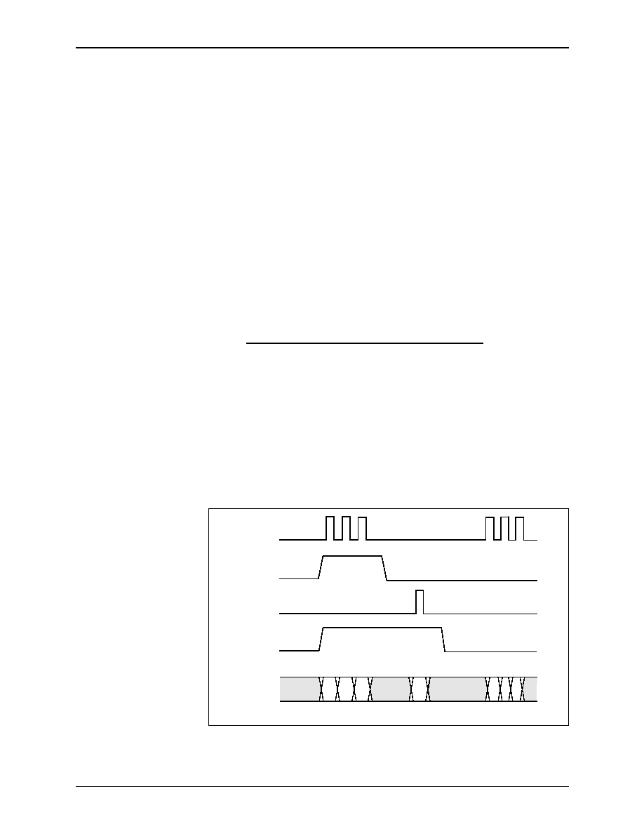
2.0 Functional Description
CN8223
2.3 Overhead Generation
ATM Transmitter/Receiver with UTOPIA Interface
2-18
Conexant
100046C
2.3.6 Receive Framing Overhead Interface
An octet interface is available for external observation of all framing overhead in
STS-1/STS-3c/STM-1 and G.832 E3/E4 framing modes. The interface consists of
two output clocks on ROVH_CLK[1,0], two output markers on RMRKR[1,0],
and an 8-bit output bus RXOVH[7:0]. Timing for this interface is illustrated in
Figure 2-13
. There is a clock pulse on the ROVH_CLK[1] output for each section
and line overhead octet in STS-1 and STS-3c/STM-1 modes and for all overhead
octets in G.832 E3 and E4 modes. There is a clock pulse on the ROVH_CLK[0]
output for each path overhead octet in STS-1 and STS-3c/STM-1 modes.
The RMRKR[1,0] outputs and the bus output are set up prior to the rising
edge of the clocks and can be sampled externally on the rising edge of
ROVH_CLK[1,0]. The RMRKR[1] output is high during row 1 overhead in all
modes (A1, A2, and C1 in STS-1/STS-3c/STM-1 modes and FA1, FA2 in G.832
E3/E4 modes). The RMRKR[0] output is high during row 1 path overhead (octet
J1) in STS-1 and STS-3c/STM-1 modes. There are two marker and clock outputs
for STS-1 and STS-3c/STM-1 modes because the SONET frame and payload
envelopes can be offset from each other.
In STS-1/STS-3c/STM-1 modes, the contents of octets D1, D2, and D3 are
provided to the internal HDLC receiver. The GC octets of the E3 and E4 formats
are also provided to the HDLC receiver. Terminal data link bits in DS3 mode (C
bits of subframe 5) and the N-bit in G.751 E3 mode are also provided to the
HDLC receiver.
Mode
Overhead Octets Output per Frame
STS-1
36
STS-3c/STM-1
90
G.832 E3
7
G.832 E4
16
Figure 2-13. Receive Framing Overhead Interface Timing
ROVH_CLK[1]
RMRKR[1]
A1
A2
C1
RXOVH[7:0]
ROVH_CLK[0]
RMRKR[0]
8223_025

CN8223
2.0 Functional Description
ATM Transmitter/Receiver with UTOPIA Interface
2.4 Status and Alarms
100046C
Conexant
2-19
2.4 Status and Alarms
The CN8223 automatically receives and generates alarms.
2.4.1 Status and Counter Interrupts
The status interrupt pin STAT_INT can be programmed to provide an interrupt on
any occurrence in the LINE_STATUS register [0x38]. Each of these signals
generates a receive status interrupt if the corresponding interrupt is enabled in the
EN_LINE_INT register [0x2D]. To determine if an interrupt is caused by a PHY
status event, the LINE_STATUS register is read. This clears the interrupts in that
register.
Two types of interrupts are provided: error and alarm. Error signals cause an
interrupt on each occurrence of an error condition. Error signals are bits 9≠13 in
the LINE_STATUS register. Alarm signals provide an interrupt on change of
state. All other indications in LINE_STATUS are alarm indications.
Interrupt status bits for the line/PHY counter overflows are located in the
OVFL_STATUS register [0x3A]. The enables for these interrupts are in
EN_OVFL_INT [0x2F]. All counters are 16 bits. If a counter is set to interrupt, it
rolls over to zero when it exceeds its maximum value. If a counter is not set to
interrupt, it saturates at its maximum value of 65,535 and ignores further events.
To determine if an interrupt has been caused by a counter, the microprocessor
reads the OVFL_STATUS register.
If the interrupt for a particular counter is not set, the counter saturates at a
value of 65,535 and stays at that value until read. If Enable One-Second Latching
of Line Counters [bit 13 in CONFIG_1 [0x00] is set, then at each one-second
interval defined by the input ONESECI, the current counter value is latched for
the following one-second interval, and the counter is cleared. If the counter is
again read in that one-second interval, the current value of the counter is read and
then cleared.
The LCV counter [0x40] is always latched (and the counter cleared) by the
ONESECI input regardless of the setting of Enable One-Second Latching of Line
Counters. When this counter is read, the latched value is presented and then
cleared. Subsequent reads prior to the next ONESECI latching event produce a
value of zero.

2.0 Functional Description
CN8223
2.4 Status and Alarms
ATM Transmitter/Receiver with UTOPIA Interface
2-20
Conexant
100046C
2.4.2 Alarm Signal Generation
Three alarm signals can be generated by the transmitter in DS3 mode. These
alarms are generated by setting Transmit Alarm Control [bits 6≠4] of the
CONFIG_2 register [0x01]. The yellow alarm is contained in the X1 and X2 bits.
DS3 AIS has the highest priority, followed by idle code, and finally yellow alarm.
DS3 FEBE alarms are generated automatically in the transmitter when the
receiver detects either a frame bit error or a C-parity error in an M-frame. When
no alarm condition is present, the FEBE channel contains all-1s. When an alarm
is to be sent (as determined by the receiver) the FEBE channel is set to all 0s for
one M-frame for each error occurrence.
In G.751 E3 mode, transmission of AIS (unframed all 1s) is enabled by setting
Transmit Alarm Control [bit 4] high. Transmission of yellow alarm is enabled by
setting Transmit Alarm Control [bit 6] high. This causes the transmitted A-bit to
be set to one.
In G.832 E3/E4 modes, transmission of AIS or the MA FERF indication is
enabled by setting Transmit Alarm Control [bits 4 or 5], respectively. The MA
timing marker bit can be set by setting Transmit Alarm Control [bit 6].
In STS-1 and STS-3c/STM-1 modes, transmission of line Alarm Indication
Signal (AIS), Line Far End Receive Failure (FERF), and various path indications
can be enabled as described in
Section 3.3
.

CN8223
2.0 Functional Description
ATM Transmitter/Receiver with UTOPIA Interface
2.4 Status and Alarms
100046C
Conexant
2-21
2.4.3 Alarm Detection
The internal framers contain status indicators to obtain alarm information for link
maintenance.
Table 2-13
shows the error indications by line mode. This table is
repeated as
Table 3-17
, in
Chapter 3.0
.
Table 2-13. Status Indications for All Modes (Register 0x38)
Bit
STS-1/STS-3c/
STM-1
Internal DS3
G.832 E3/E4
Internal G.751 E3
Ext. Framer
(57 octet)
15
Line FEBE Error
0
0
0
0
14
One-Second Count
One-Second Count
One-Second Count
One-Second Count
One-Second Count
13
Signal Label
Mismatch
Invalid FEBE
Payload Type
Mismatch
Invalid FEBE
Invalid FEBE
12
Path FERF Error
FEBE All 1s
MA FERF
FEBE All 1s
FEBE All 1s
11
Path FEBE Error
PLCP FEBE Error
MA FEBE
PLCP FEBE Error
PLCP FEBE Error
10
Summary BIP Error
PLCP BIP Error
EM BIP Error
PLCP BIP Error
PLCP BIP Error
9
Line FERF
PLCP Frame Error
x
PLCP Frame Error
PLCP Frame Error
8
LOC
PLCP Yellow/LOC
LOC
PLCP Yellow
PLCP Yellow
7
STS LOF 2≠3
PLCP LOF 2≠3
E3/E4 LOF 2≠3
PLCP LOF 2≠3
PLCP LOF 2≠3
6
STS LOF
PLCP LOF
E3/E4 LOF
PLCP LOF
PLCP LOF
5
STS OOF
PLCP OOF/LOC
E3/E4 OOF
PLCP OOF
PLCP OOF
4
Path Yellow
DS3 X-bit Yellow
x
E3 A-bit Yellow
x
3
Path AIS
DS3 Idle Code
x
x
x
2
Line AIS
DS3 AIS
E3/E4 AIS
E3 AIS
x
1
STS LOP
DS3 OOF
x
E3 OOF
x
0
LOS (Input)
LOS (Input)
LOS (Input)
LOS (Input)
LOS (Input)
NOTE(S):
"x" means content should be disregarded.

2.0 Functional Description
CN8223
2.5 Parallel Line Interface
ATM Transmitter/Receiver with UTOPIA Interface
2-22
Conexant
100046C
2.5 Parallel Line Interface
The CN8223 has a parallel line interface consisting of TXOUT[8:0] and
RXOUT[8:0]. These octet ports allow interfacing of external framers or other
devices that use parallel data.
Table 2-1
, illustrates the architecture of this parallel
interface. Also, this interface can be used for the Advanced Micro Devices TAXI
interface chipset.
2.5.1 TAXI Interface
The parallel port of the CN8223 can be configured to interface directly with
AMD's TAXI transmit/receive chipset. To enable this mode, set the following
values in each of these registers:
The transmit interface logic automatically generates the signals needed by the
TAXI transmitter to insert JK sync and TT start-of-cell symbols before each
transmitted data cell of 53 octets. When no transmit port is active, the transmitter
sends continuous JK sync symbols.
The receiver interface logic detects the TT start-of-cell command and
synchronizes its cell circuitry to receive and process the 53-octet cell data. The
receiver ignores all incoming JK sync signals while awaiting the reception of the
TT symbol. The receiver is not clocked on any command or data octet if the
violation indication is present on RXIN[8]. None of the indications in the
LINE_STATUS register [0x38] are valid in TAXI mode except for One Second
Count. Any other indications should be ignored. Violations will be counted in
Line Counter 2. All cell status and cell event counters operate as in other modes.
In TAXI mode, the capability to shut down the output of cells to the FIFO
interface is lost because of the use of the RCV_HLD pin. In this mode, the control
bits in CELL_VAL or external logic using the VLTN signal must be employed for
this function.
NOTE:
Source and line loopbacks are not functional in TAXI mode due to the
asymmetry between the transmit and receive control lines.
CONFIG_1 (0x00):
Set the 8 LSBs to 0xE0.
CONFIG_3 (0x02):
Set Enable HEC Coset (bit 0) and Invert RX Clock
(bit 8) high.
CONFIG_4 (0x29):
Set Enable TAXI Interface (bit 3) high.

CN8223
2.0 Functional Description
ATM Transmitter/Receiver with UTOPIA Interface
2.5 Parallel Line Interface
100046C
Conexant
2-23
Timing information for TAXI mode is found in
Section 4.3.5
. Pin connections
for the TAXI chipset and the CN8223 are listed in
Table 2-14
.
2.5.2 Transmit Parallel Interface
Interface connections for the Transmit Parallel Interface mode are listed in
Table 2-15
. TXOD and TXDELO are mapped to TXIN and TXOUT[8],
respectively.
Figure 2-14
illustrates the transmit timing for the parallel interface.
TXCKI has a frequency of up to 20 MHz. In parallel mode, the synchronization
signal TXOD marks the octet clocks where the CN8223 does not provide a new
data octet on the TXDAT output. This could be used for marking all of the
overhead (non-ATM payload) octets in a data stream.
Alternatively, TXOD can be held low and a gapped octet clock provided from
the external circuitry to the CN8223 on TXCKI. TXDAT is the output signal; it
transitions in response to the rising edge of TXCKI, and can be sampled on the
following falling edge externally. TXDELO also transitions in response to the
rising edge and marks the first octet of each 53-octet cell.
Table 2-14. Pin Connections between TAXI Chipset and CN8223
Signal Name from TAXI Chipset
Connect to CN8223 Pin
Receive Clock (CLK)
RXCKI
Receive Data (DO 7-0)
RXIN[7:0]
Receive Command (CO 1)
TXIN
Receive Command Strobe (CSTRB)
RCV_HLD
Receive Violation (VLTN)
RXIN[8]
Transmit Clock (CLK)
TXCKI
Transmit Data (DI 7-0)
TXOUT[7:0]
Transmit Command (CI 1)
TXOUT[8]
Transmit Command (CI 0,2,3)
GND
Transmit Strobe (STRB)
TCLKO
Table 2-15. Transmit Parallel Interface Mode Connections
Signal Name
Connect to CN8223 Pin
Transmit Clock Input (TXCKI)
TXCKI
Transmit Octet Disable (TXOD)
TXIN
Transmit Data Output (TXDAT)
TXOUT[7:0]
Transmit Cell Delineation (TXDELO)
TXOUT[8]
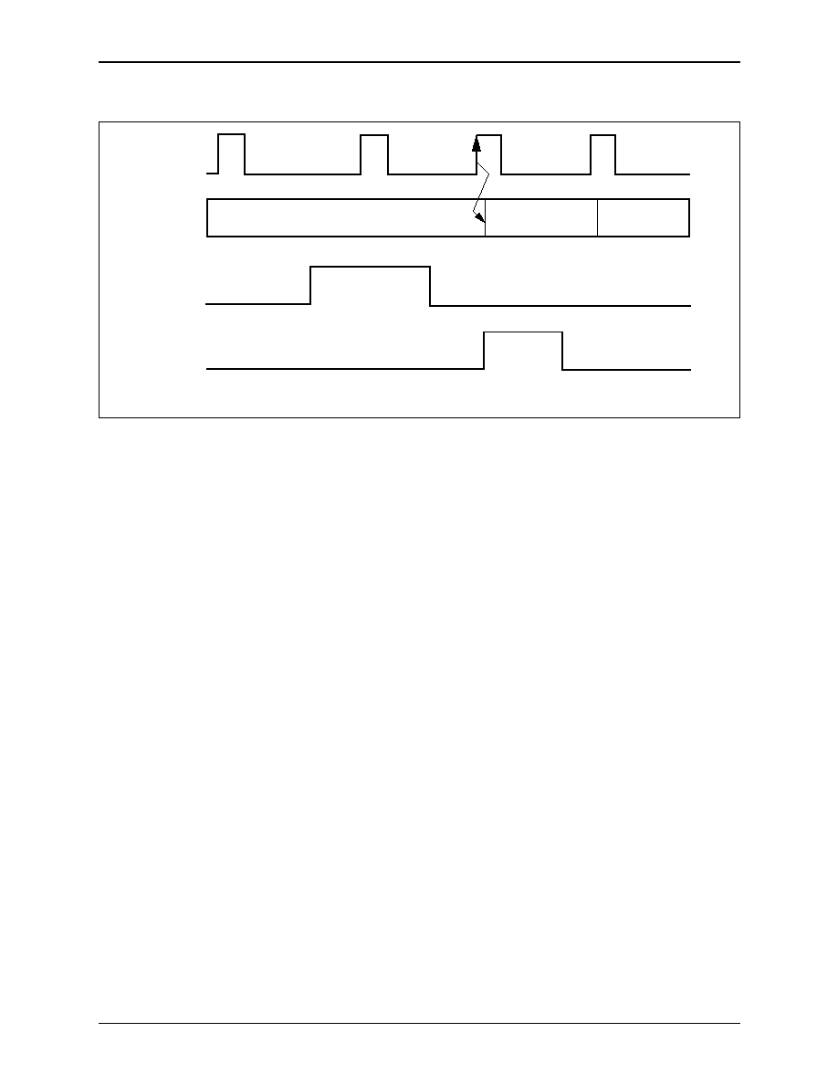
2.0 Functional Description
CN8223
2.5 Parallel Line Interface
ATM Transmitter/Receiver with UTOPIA Interface
2-24
Conexant
100046C
Figure 2-14. Transmit Parallel Interface Timing
TXCKI
TXDAT[7:0]
TXOD
Data
Data
Data
TXDELO
8223_026
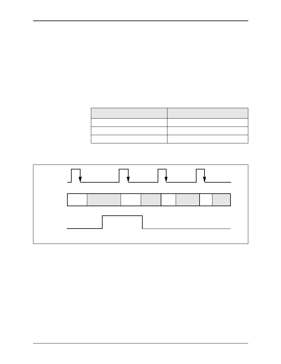
CN8223
2.0 Functional Description
ATM Transmitter/Receiver with UTOPIA Interface
2.5 Parallel Line Interface
100046C
Conexant
2-25
2.5.3 Receive Parallel Interface
Interface connections for the Receive Parallel Interface mode are listed in
Table 2-16
.
Figure 2-15
illustrates the receive timing for the parallel interface. In
parallel mode, data octets are provided on RXDAT[7:0] with an octet clock (up to
20 MHz) on RXCKI. The octet data is sampled on the falling edge of RXCKI.
The data inputs can be sampled on the rising edge of the input clock by setting
Invert RX Clock Sampling [bit 8] of CONFIG_3 [0x02]. An idle octet indicator
can be provided on RXOD as illustrated in
Figure 2-15
. The CN8223 ignores all
octets for which the RXOD input is high. This input can be used to mark framing
overhead (non-ATM payload) octets.
Table 2-16. Receive Parallel Interface Mode Connections
Signal Name
Connect to CN8223 Pin
Receive Clock Input (RXCKI)
RXCKI
Receive Octet Disable (RXOD)
RXIN[8]
Receive Data Input (RXDAT)
RXIN[7:0]
Figure 2-15. Receive Parallel Interface Timing
RXCKI
RXDAT[7:0]
RXOD
Data
Data
(ignored)
Data
Data
8223_027

2.0 Functional Description
CN8223
2.6 ATM Cell Processing
ATM Transmitter/Receiver with UTOPIA Interface
2-26
Conexant
100046C
2.6 ATM Cell Processing
The ATM cell processing block is located between the line framers and FIFO port
blocks of the CN8223 (see
Figure 1-3
). This functional block interfaces between
the octet data and cell data portions of the chip. The CN8223 supports cell
delineation via either PLCP or HEC alignment for DS1, E1, DS3, E3, E4, STS-1,
and STS-3c/STM-1 rates. At DS3 and E3 rates, all required stuffing functions are
supported.
2.6.1 Cell Generation for Transmit
Cell generation refers to the formatting of 53-octet ATM cells from 48- or
52-octet payload data from the FIFO interface for hand-off to the line framer
transmitter. The CN8223 provides modes that generate complete cells as well as
modes that pass entire 53- or 57-octet cells directly from the FIFO interface. Cell
modes and other per-port controls are in the four CELL_GEN_x registers
[0x04≠0x07].
The generation process operates autonomously with a handshake protocol
through the FIFO interface. Cells are forwarded automatically to the line framer
for transmission.
When full ATM cell generation is performed, a 5-octet header is generated by
the CN8223. The VCI and other fields in the first 4 octets come from
microprocessor control registers. The HEC in octet 5 is calculated and inserted by
the CN8223. HEC coverage over 4-header octets (ATM) or 3-header octets
(SMDS/802.6) is selectable by HEC Coverage [bit 1] of CONFIG_3 [0x02]. The
remaining 48 octets are payload and are taken from the FIFO interface. The
CN8223 calculates and overwrites the CRC field to complete the 53-octet cell.
A cell-ready indication controls the cell generation process from the external
ATM interface circuit to the cell generation block. When the ATM interface
indicates that it has the first cell of a message ready, the cell generation block
begins formatting a non-idle cell for transmission using the octet data and cell
delineation control inputs at the interface. The cell generation circuitry
automatically generates idle cells until the external FIFO indicates that another
cell is ready for transfer. The header and payload for idle cells are programmable
via control registers. When the next cell is ready, the host presents the data and
cell delineation control inputs.

CN8223
2.0 Functional Description
ATM Transmitter/Receiver with UTOPIA Interface
2.6 ATM Cell Processing
100046C
Conexant
2-27
Two rate control registers are provided for control of the port sources to allow
programmable rate shaping of cell transmission. The ratio of active to idle cells is
programmable with 0.4 % granularity. The cell generation process maintains
status counts of non-idle cells transmitted for each of the four sources.
Table 2-17
lists the four cell generation modes provided by the CN8223.
2.6.1.1 CELL_GEN_x
Register
Per-port cell generation registers for FIFO Ports 0≠3 are in the four
CELL_GEN_x registers [0x04≠0x07]. Cell Generation Mode [bits 1,0] selects the
operating mode for the generation circuit. The four modes described in
Table 2-17
are provided. In 52-, 53-, or 57-octet modes, the individual header fields obtained
from the FIFO interface can be overwritten. This overwriting is accomplished
with the values found in the TX_HDR registers for a particular port by setting the
appropriate field insertion control bit in the CELL_GEN_x register. In 48-octet
mode the header fields always come from the programmed value in the
corresponding TX_HDR register.
The overhead fields of active cells are taken from the locations listed in
Table 2-18
or set to the indicated values.
Table 2-17. Cell Generation Modes
Mode
Function
48-Octet Mode
Provides for full ATM generation. Forty-eight octets are taken from the FIFO interface, the appropriate
header fields are attached, and the payload CRC is overwritten to form the ATM cell.
52-Octet Mode
Allows a 53-octet cell, less the HEC octet, to be transferred from the FIFO interface. The HEC is calculated
and inserted by the CN8223. The payload CRC for AAL3/4 can be inserted, or checked and transferred
without modification. Both the HEC and the payload CRC can be optionally disabled or errored on a
single-event basis. The cell generation process also provides HEC coset generation, ATM payload
scrambling. In each of the above modes, any header field can be overwritten with information from
control registers.
53-Octet Mode
Allows entire 53-octet cells to be transferred from the FIFO interface. This is the mode used when Port 0
is configured for UTOPIA.
57-Octet Mode
Allows the input of entire 57-octet PLCP slots from the FIFO interface. Can be used for external PLCP
insertion or test generation purposes.

2.0 Functional Description
CN8223
2.6 ATM Cell Processing
ATM Transmitter/Receiver with UTOPIA Interface
2-28
Conexant
100046C
Disable HEC [bit 9] and Disable Payload CRC [bit 10] in the CELL_GEN_x
registers [0x04≠0x07], disable the field generation and allow the existing field to
pass. Error HEC [bit 11] and Error Payload CRC [bit 12] force a single error
occurrence in the generated field. The Error functions are cleared after the error
is generated. This allows the microprocessor to easily generate a specific number
of errors. The error pattern programmed in the TXFEAC_ERRPAT register
[0x03] is used with the Error HEC control to generate a specific number of HEC
errors for checking receiver error correction/detection circuitry.
The Error Payload CRC bit inserts 4-bit errors into the payload CRC field.
The Inhibit Single Cell Generation [bit 13] field in CELL_GEN_x, inhibits cell
transmission from the port for a single cell interval. A single idle cell (with header
contents as defined in the Transmit Idle Header Register [0x0A≠0x0B] and
payload set to all 0s) is transmitted in place of a data cell from this port at the next
cell interval if the priority control tries to obtain a cell from this port. This bit is
cleared by the cell generation circuitry after the idle cell has been transmitted or if
a cell from another port is selected by the priority control. The microprocessor
can poll this bit to determine when the idle cell insertion has been completed.
Idle cells are automatically generated when no transmit port is active. The
header for idle cells is obtained from the TX_IDLE_xx registers, and the HEC is
automatically calculated. The payload for idle cells is obtained from the
IDLE_PAY register [0x2A]. This data octet is inserted in all octet positions of the
idle cell payload. The CRC-10 can be inserted if required by setting Disable
Payload CRC of CELL_GEN_x to zero.
2.6.1.2 Cell Generation
Status and Status
Interrupts for Transmit
A per-port count of cells transmitted is maintained in the CELL_SENT_CNTx
counters [0x4E≠0x51] for each port. These counters can be programmed to cause
an interrupt in the CELL_STATUS register [0x3B] by setting enable bits in the
EN_CELL_INT register 0x30]. The interrupt clears when CELL_STATUS is
read. If the counter interrupt is not enabled, the counter stops at its maximum
value of 65,535. If the interrupt is enabled, the counter interrupts on "roll over"
and continues counting. The counter clears when it is read.
Table 2-18. Overhead Field Locations
Overhead Field
Source
Cell Header
Header Register TX_HDR or FIFO input
Header Error Control
HEC Generation Circuit or FIFO input
Segment Type
FIFO Input
Sequence Count
FIFO Input
Length Field
FIFO Input
Payload CRC
Payload CRC Generation Circuit or FIFO Input

CN8223
2.0 Functional Description
ATM Transmitter/Receiver with UTOPIA Interface
2.6 ATM Cell Processing
100046C
Conexant
2-29
2.6.2 Cell Validation for Receive
Cell validation refers to the checking of cells coming in from the PHY block for
proper format. Modes that deliver 48-, 52- or 53-octet cells, or 57-octet PLCP
slots to the FIFO output ports are provided by the CN8223.
Four modes are available for cell output:
∑
A test mode writes the entire 57-octet PLCP slot to the FIFO interface.
∑
A 53-octet mode writes the 53-octet ATM cell to the FIFO interface.
∑
A 52-octet mode writes the ATM cell without the HEC octet to the FIFO
interface.
∑
A final mode delivers 48-octet cell payloads to the FIFO interface.
When the UTOPIA interface mode is used, only 53-octet output is available.
The protocol verification provided includes HEC validation with ATM or
SMDS/802.6 coverage, cell header filter/screen against four maskable 32-bit
programmable values, validation of payload length per segment type, and correct
payload CRC value. Status reporting on validation steps is via error counters and
status register indications. Status bits can be programmed to generate interrupts to
the microprocessor. Each validation step can be individually disabled. Cells are
routed to one of four output ports if a match to that port's programmable header
value is made.
Each cell is output to the ATM interface after a 6- or 10-octet buffer to allow
for header processing. A "cell-valid" output pin is provided to indicate that none
of the enabled error checks detected an error. The UTOPIA internal FIFO or
external circuitry is notified to discard the cell when the valid indication goes
inactive. Idle cells are automatically deleted from the ATM layer output. Parity
and control/delineation signals are provided with each octet at the port interface.
The microprocessor receives status and error counts as cell validation proceeds.
All event and error counters can be programmed to cause an interrupt on
overflow. Reading the interrupt source register allows the microprocessor to
identify overflows and update internal counts. All counters can be read by the
microprocessor and are cleared when read.

2.0 Functional Description
CN8223
2.6 ATM Cell Processing
ATM Transmitter/Receiver with UTOPIA Interface
2-30
Conexant
100046C
2.6.2.1 HEC Alignment
In 53-octet mode, either the internal framer or the parallel input provides octet
alignment information to the HEC alignment state machine. Each octet position is
then searched for correct HEC alignment to determine cell delineation. The HEC
alignment framing state machine is given in ITU I.432. Three states are present:
hunt, pre-sync, and sync. The hunt state is entered when seven consecutive
errored HEC patterns are found at the current alignment location. The pre-sync
state is entered when a candidate position contains the correct HEC pattern. The
sync state is entered when six consecutive, correct HEC patterns at the candidate
location are found.
The HEC state machine can be altered to include state integration by setting
the Integrate HEC Framing control bit in CONFIG_5. When this bit is set, the
state machine has two additional states: OCD Anomaly and Verification. The
OCD Anomaly state is entered when seven consecutive errored HEC patterns are
found at the current alignment location. OCD Anomaly status is indicated in bit
10 of CONFIG_5. After an integration time of X ms in the OCD Anomaly state,
the LCD defect state is entered. The LCD defect state is indicated in bit 8 of
LINE_STATUS [0x38] and on the LOCD output pin. The verification state is
entered when six consecutive, correct HEC patterns at the candidate location are
found. After x ms in the verification state, the sync state is entered. The value of x
is 4 ms for SONET/SDH modes and 2.5 ms for DS3 mode. This integration time
is counted from the 8 kHz reference input on the 8KCKI input pin. A rising edge
must be present on this input every 125
µs for proper integration in this state
machine.
2.6.2.2 CELL_VAL
Control Register
Cell validation refers to the error checking of received cells prior to output to the
FIFO interface. It is controlled via the CELL_VAL register [0x14]. Per-port
output mode selects 48-, 52-, 53-, or 57-octet modes for each of the four ports.
Enable HEC Correction [bit 8] enables the HEC correction mode for single-bit
header errors. If this bit is set to zero, then no correction is performed, but error
detection is always performed. Error correction must be disabled if HEC
Coverage [bit 1] in CONFIG_3 [0x03] is set for SMDS/802.6 mode, or if Enable
HEC Coset [bit 0] in CONFIG_3 is not enabled.
Header Only Output [bit 12] in CELL_VAL enables a 5-octet output mode on
Port 3. Only the 4 header octets of cells addressed to Port 3 and the status octet in
Table 2-19
are output to the FIFO port. In 53-octet cell formats, if status output is
enabled with Header Only Output, none of the other ports should be programmed
for 53-octet output.
Enable Status Octet [bit 13] in CELL_VAL sends a status octet to FIFO Port 3.
It should only be used in 53-octet output mode. When this bit is set, the HEC octet
position in the FIFO output data is omitted, and a status word as shown in
Table 2-19
is appended to the end of the cell as octet number 53. In 53-octet cell
formats, if status output is enabled with the Enable Status Octet bit, none of the
other ports should be programmed for 53-octet output.
The status word contains indications of Port 3 header and payload errors as
well as VCI/VPI match information for the other three ports for each cell
received. The status word bits are set only if the corresponding failure occurs and
the check for that failure is enabled. The User Data Bit is derived from the PT
field in the header as shown in
Table 2-20
and can be used as an AAL5 EOM
marker. These two Port 3 output options are available only if none of the ports are
set to 57-octet output mode.

CN8223
2.0 Functional Description
ATM Transmitter/Receiver with UTOPIA Interface
2.6 ATM Cell Processing
100046C
Conexant
2-31
If Disable Cell Receiver [bit 14] of CELL_VAL and Disable Port Reception--
Port X [bits 7≠4] of CONFIG_4 [0x29] are not set, then enabled checks are made
on each cell received in the following sequence:
1.
The HEC is checked for errors under control of the HEC Coverage [bit 1]
of CONFIG_3 [0x03]. Correctable errors are corrected if Enable HEC
Correction [bit 8] of CELL_VAL is set. The correction/detection state
machine is implemented as defined in the ATM UNI/NNI specifications.
Errors counted in either the COR_HEC_ERR counter [0x49] or
UNCOR_HEC_ERR counter [0x4A] are also indicated in the
corresponding bits in the EVENT_STATUS register [0x39]. HEC error
correction/detection is performed independent of any header screening that
is enabled. Error correction should be enabled only if HEC Coverage is 0
and Enable HEC Coset [bit 0] of CONFIG_3 is 1.
2.
The payload CRC-10 is checked. Errors are counted in the
PAY_CRC_ERR counter [0x48] and indicated in EVENT_STATUS. No
CRC checking is performed on cells matching the idle header description.
3.
The payload length is checked to be consistent with the segment type.
Table 2-19. Status Octet Definition
Bit
Definition
0
HEC Error Corrected for Port 3
1
HEC Error Not-Corrected for Port 3
2
Payload Length Error for Port 3 (AAL3/4)
3
Payload CRC-10 Error for Port 3 (AAL3/4)
4
User Data Bit for Port 3 (AAL5 EOM)
5
Header Match Port 0
6
Header Match Port 1
7
Header Match Port 2
Table 2-20. PT Header Field and User Data Bit
PT Header Field
User Data Bit
0 0 0
0
0 0 1
1
0 1 0
0
0 1 1
1
1 0 0
0
1 0 1
0
1 1 0
0
1 1 1
0

2.0 Functional Description
CN8223
2.6 ATM Cell Processing
ATM Transmitter/Receiver with UTOPIA Interface
2-32
Conexant
100046C
.
Errors are counted in the PAY_LEN_ERR counter [0x4C] and indicated in
EVENT_STATUS. No payload length checking is performed on cells
matching the idle header description.
All errors disabled by the global disables in CELL_VAL are counted, and the
first enabled error in the above sequence of checks is counted in the appropriate
cell error counter. Disabled errors will not cause the cell to be marked as invalid.
Header octets are compared to the HDR_VAL registers under control of the
HDR_MSK bits. This determines routing to the proper output port. If no match is
made to any of the VCI/VPI fields for the four ports or to the idle definition, the
cell is counted in the NON_MATCH_CNT counter [0x57]. Payload CRC-10 and
length checks can also be disabled on a per port basis by using the control bits in
CONFIG_4. These bits simply disable the error from marking the cell as invalid
and do not affect the counting of errors in any way. This feature can be used to
route AAL 3/4 cells to one port with checks enabled and AAL5 cells to a different
port with checks disabled.
HEC Coverage [bit 1] in CONFIG_3 determines the calculation range for the
HEC. If this bit is low, the HEC is calculated over header octets 1≠4 for ATM
cells. If this bit is high, the HEC is calculated over header octets 2≠4 for
SMDS/802.6 cells.
Validation checks can be individually disabled with the remaining control bits
in the CELL_VAL register [0x14]. Disable HEC Check [bit 9] disables the check
of the header error control octet. Disable Payload Length Check [bit 10] disables
the check for consistency between the segment type field and the length field.
Disable Payload CRC Check [bit 11] disables the check of the payload CRC. The
above disables are global disables for all ports and override the per-port control in
CONFIG_4, which also contains per port disables for payload length and payload
CRC checks.
2.6.2.3 Interrupts and
Status Counters for Cell
Validation
Cell error events are indicated with bits 0≠6 of the EVENT_STATUS register
[0x39] and can cause an interrupt if enabled with the corresponding bit in the
EN_EVENT_INT register [0x2E]. Status bits are latched at the event occurrence
and are cleared when EVENT_STATUS is read. The error events are also
counted, and interrupts on error counter overflows can be enabled in
EN_OVFL_INT [0x2F]. Counter overflow status is provided in OVFL_STATUS
[0x3A], and the status bits are cleared when the status register is read. These
counters are not latched, and each counter is cleared individually when it is read.
CELL_RCV_CNTx [0x52≠0x55] provides a count of all cells that are
accepted for processing and delivery to Port x. This count is based on a header
match with the header value and mask bits that are set in the associated registers
for Port x. This count does not include cells discarded due to an error in the HEC.
IDLE_CELL_CNT [0x56] is a count of valid cells received that match the
programmed idle value and mask. NON_MATCH_CNT [0x57] is a count of
active cells that did not match any of the programmed VCI/VPI values (port or
idle).
Segment Type
Payload Length
BOM or COM
44
EOM
4≠44 mod 4
SSM
8≠44 mod 4

CN8223
2.0 Functional Description
ATM Transmitter/Receiver with UTOPIA Interface
2.6 ATM Cell Processing
100046C
Conexant
2-33
Counter overflow interrupts can be individually enabled. If a counter is set to
interrupt, it rolls over to zero, sets the interrupt, and continues counting errors
after it reaches its maximum value. If a counter is not set to interrupt, it saturates
and holds when it reaches its maximum value (0xfff). The interrupt enable bits for
the counters are found in the EN_CELL_INT register [0x30], with the
corresponding interrupt status in the CELL_STATUS register [0x38]. If one of
the cell counter overflow interrupts occurs, the CELL_STATUS register can be
read to determine which counter or counters overflowed. These interrupts are
cleared when CELL_STATUS is read.
Some interrupts in the CELL_STATUS register are related to the
transmission/reception of individual cells. These interrupts may be enabled in
EN_CELL_INT with corresponding status bits in CELL_STATUS. Cell
Rcvd--Port x indicates the validation process has received a complete ATM cell
destined for Port x. Cell Sent--Port x indicates a cell has been transmitted from
source x. These interrupts are cleared when CELL_STATUS is read.
2.6.3 PLCP Cell Generation for Transmit
In 57-octet PLCP formats, the PLCP overhead generation consists of the framing
octets A1 and A2, the Path Overhead Identifier (POI) octets, and the path
overhead octets. All of these are generated by the PHY transmit circuitry, but can
be selectively disabled if desired.
The A1 and A2 octets are generated according to TR-TSV-000773. The POI
octets are determined by the particular PLCP that is selected, but in each case they
consist of a slot count and a parity bit. The DS3 PLCP has 12 slots per frame, the
DS1 and E1 PLCP have 10, and the E3 PLCP has 9. In each case, the POI octets
provide a backwards count of the PLCP slots in the frame, along with a parity bit.
Generation of the A1, A2, and POI octets can be disabled via the Overhead
Control [bits 3≠0] of CONFIG_2 [0x01]. All path overhead growth octets Zn and
the path user channel F1 are forced to zero.
The B1 octet is populated with a BIP-8 code that is calculated over each PLCP
frame. The BIP Error Insert [bits 12≠10] of CONFIG_2 control insertion of BIP-8
errors in the generated PLCP. If errors are to be inserted, a non-zero value written
to the TXFEAC_ERRPAT register inverts the corresponding bits of the B1 octet
from that calculated by the BIP-8 circuit in the following PLCP frame. Insert
control bits are cleared after each frame when the errors are inserted. The register
can be read to determine if this has occurred, so that the microprocessor can insert
BIP-8 errors as desired in each PLCP frame.

2.0 Functional Description
CN8223
2.6 ATM Cell Processing
ATM Transmitter/Receiver with UTOPIA Interface
2-34
Conexant
100046C
This capability can be used to verify far-end FEBE operation. BIP generation
can be disabled via the Overhead Control bits. The fields of the G1 octet are
under control of the All 0s FEBE [bit 14], All 1s FEBE [bit 13], and Transmit
Alarm Control [bits 9≠4] of CONFIG_2. The FEBE controls operate as shown in
Table 2-21
.
The yellow alarm bit in the G1 octet is set to the value contained in Transmit
Alarm Control [bit 7].
The C1 octet is under control of PHY Type [bits 2≠0] of CONFIG_1 [0x00],
Force Cycle Stuffing [bit 6] of CONFIG_3 [0x02], and Overhead Control [bits
3≠0] of CONFIG_2 [0x01] as shown in
Table 2-22
.
The trailer content (except in E1 mode where there is no trailer) has each
nibble set to 1100 unless Overhead Control [bit 0] is set. In this case, each nibble
has the value 0000.
In 53-octet formats, no PLCP overhead is associated with each ATM cell. The
only overhead present is that contained in the line framing format, as discussed in
Section 2.2
.
Table 2-21. FEBE Controls
All 1s FEBE
All 0s FEBE
FEBE Field Value
0
0
BIP-8 Errors Received
0
1
0000
1
0
1111
1
1
0000
Table 2-22. C1 Octet
Disable C1
Generation
PHY Type
Force Cycle
Stuffing
C1 Octet Value
1
x
x
00
0
DS1, E1
x
00
0
DS3, E3
0
Per Selected 8 kHz Reference
(Via CONFIG_1, Bit 11)
0
DS3, E3
1
Per Default Cycle

CN8223
2.0 Functional Description
ATM Transmitter/Receiver with UTOPIA Interface
2.6 ATM Cell Processing
100046C
Conexant
2-35
2.6.4 PLCP Cell Validation for Receive
In 57-octet PLCP formats, the PHY receiver implements framing state machines
for cell alignment as described in TR-TSV-000773. In 53-octet formats, the PHY
receiver implements the HEC alignment state machine as described in ITU I.432.
In serial framed 57-octet mode, the PHY receiver processes a serial stream to
find PLCP framing. Octet synchronization is provided externally in DS1 and E1
modes. Internal or external E3 octet synchronization and DS3 nibble
synchronization are provided to the PHY framer. Physical layer framing patterns
are automatically removed before recovery of the octet data. If unframed mode is
enabled, the receiver will search each bit position to determine octet alignment.
The 57-octet PLCP framing state machine contains three states: in-frame,
out-of-frame, and loss-of-frame. Valid framing is found when two consecutive
valid path overhead octets in sequence are observed after the A1, A2 framing
octets. The out-of-frame state is entered only from the in-frame state, when there
are errors in both the A1 and A2 octets or when there are two consecutive Pn
errors. This event is an OOF event, and is counted. The LOF state is entered after
eight consecutive PLCP frames in the out-of-frame state.
Stuffing and destuffing are provided according to the PHY type setting in
57-octet formats. Cycle stuffing is used at the transmit PLCP for DS3 and E3
whenever the receive PLCP is in the LOF state or the RCV_HLD input is high,
and this function is enabled with Receiver Hold Enable [bit 10] of CONFIG_1
[0x00]. Cycle stuffing can also be forced by setting Force Cycle Stuffing [bit 6]
of CONFIG_3 [0x02] high.
NOTE:
When the framing mode is dynamically modified between direct mapping
and PLCP framing, the CN8223 will go into an OOF state. Dynamic
switching should only be used if necessary.
2.6.4.1 PLCP Status
Errors in either the A1 or A2 PLCP framing octets cause an indication in the
LINE_STATUS register PLCP Frame Error bit and are counted. PLCP OOF
events are indicated by the PLCP OOF bit and counted. PLCP LOF events (OOF
for eight consecutive PLCP frames) are indicated by the PLCP LOF bit. If an
LOF condition persists for more than 2≠3 seconds, the PLCP LOF 2≠3 status bit
is set. This is determined by LOF being set for three consecutive rising edges of
the ONESECI input. Loss of cell delineation in 53-octet modes is indicated by the
LOC bit and counted. PLCP OOF and LOC indications also appear on the LOCD
output pin.
The PLCP Yellow Alarm status bit is set high after 10 consecutive frames with
a PLCP yellow alarm value of one and cleared after 10 consecutive frames of a
value of zero.
Errors detected in the receiver BIP-8 code checking circuit cause BIP-8 Error
to be set and counted. FEBE Error is set if any valid non-zero FEBE value (values
of 1 through 8) is received. This condition is also counted in the REM_BIP
counter. Invalid FEBE is set if any invalid FEBE value (9 through F) is received; a
value of F also causes FEBE All 1s to be set. This value is used to indicate that
the FEBE calculation is not supported at the far end of the circuit.

2.0 Functional Description
CN8223
2.6 ATM Cell Processing
ATM Transmitter/Receiver with UTOPIA Interface
2-36
Conexant
100046C
Each rising edge at the ONESECI input causes an indication in the
One-Second Count bit. This indication can be used as a timing interrupt to
coordinate status collection. If Enable One-second Latching of Line Status is set,
the ONESECI input also causes status indications in LINE_STATUS to be
latched. If an alarm condition is present during a one-second interval, it is
available to be read on the successive interval. Otherwise, the status is latched and
held until it is read. If this bit is set and the status word is read twice within a
one-second interval, the second read gives the current state of the status word and
clears the status register. Enable One-second Latching of Line Counters provides
the same functionality for the counters.
Each of the LINE_STATUS bits is latched until read and then cleared if the
condition is no longer present. If a status condition clears before the register is
read, the status bit is still held. Current status can be obtained by reading the
register twice in succession.
2.6.5 PLCP Transmit/Receive Synchronization
For 57-octet formats, the PLCP block must transmit segments at the same rate as
they are received. For DS1 and E1, long-term synchronization of the bit clock
rates establish this. For DS3 and E3 rates, the payload data rate is independent of
the line rate, and a separate timing/synchronization mechanism is required.
The DS3 and E3 PLCPs both have a 125 µs frame period. The reference clock
for this frame is taken from the received signal, or alternatively from an external
reference supplied to the 8 kHz clock input 8KCKI. In either case, the transmit
circuit generates one PLCP frame per reference frame.
In 53-octet formats, all frame structures are based on a 125
µs period;
consequently, no stuffing is required to synchronize the transmit and receive
segments.
Clock and control inputs consist of the following:
∑
An external 8 kHz reference for the PLCP at E3 and DS3
∑
A one-second input to synchronize status collection timing in
multiple-port applications
∑
A "hold receiver" input that can externally disable cell validation when an
external framer loses frame or signal
∑
Three test inputs
∑
A reset input
A one-second clock output is provided to allow synchronization of status
collection for multiple CN8223s or for CN8223s and framers. When a single
CN8223 is used, ONESECO should be connected to ONESECI. This timing
output is derived from the external 8 kHz reference clock input on 8KCKI.

CN8223
2.0 Functional Description
ATM Transmitter/Receiver with UTOPIA Interface
2.7 FIFO Port/UTOPIA Interface
100046C
Conexant
2-37
2.7 FIFO Port/UTOPIA Interface
The CN8223 has four bidirectional FIFO ports used to interface to the ATM layer
outside the chip. These four ports share FDAT_IN and FDAT_OUT 8-bit ports.
Each port has its own set of six control signals used for flow control and timing.
(Refer to
Figure 1-4
, for a diagram of the FIFO port/UTOPIA interface.)
Port 0 can be configured as a level 1 compliant UTOPIA port for connection
to other UTOPIA components. When UTOPIA mode is enabled, Ports 1, 2, and 3
are unused. The UTOPIA interface is detailed in
Section 2.7.5
.
2.7.1 FIFO Interface Inputs and Outputs
The four-port FIFO interface allows the connection of the CN8223 directly to
dual-port RAMs, FIFO RAMs, and other similar circuits. The FIFO interface pins
and their functions used for connection are listed in
Table 2-23
. Transmit FIFO
port timing for the 53-octet mode is shown in
Figure 2-16
. Detailed descriptions
of the transmit FIFO pin functions are given in
Table 2-24
. Receive FIFO port
timing for the 53-octet mode is shown in
Figure 2-17
. Detailed descriptions of the
receive FIFO pin functions are given in
Table 2-25
.
Table 2-23. FIFO Interface Pin Connections (1 of 2)
CN8223
Function
FDAT_IN[8:0]
Transmit Data with Parity
FCTRL_IN[0]
Port 0 Transmit Data FIFO Empty
FCTRL_IN[1]
Port 1 Transmit Data FIFO Empty
FCTRL_IN[2]
Port 2 Transmit Data FIFO Empty
FCTRL_IN[3]
Port 3 Transmit Data FIFO Empty
FCTRL_IN[4]
Port 0 Receive Data FIFO Full
FCTRL_IN[5]
Port 1 Receive Data FIFO Full
FCTRL_IN[6]
Port 2 Receive Data FIFO Full
FCTRL_IN[7]
Port 3 Receive Data FIFO Full
FDAT_OUT[8:0]
Receive Data with Parity
FCTRL_OUT[0]
Port 0 Receive Data Write Strobe
FCTRL_OUT[1]
Port 1 Receive Data Write Strobe
FCTRL_OUT[2]
Port 2 Receive Data Write Strobe
FCTRL_OUT[3]
Port 3 Receive Data Write Strobe
FCTRL_OUT[4]
Port 0 Receive Cell Invalid Indication
FCTRL_OUT[5]
Port 1 Receive Cell Invalid Indication
FCTRL_OUT[6]
Port 2 Receive Cell Invalid Indication

2.0 Functional Description
CN8223
2.7 FIFO Port/UTOPIA Interface
ATM Transmitter/Receiver with UTOPIA Interface
2-38
Conexant
100046C
FCTRL_OUT[7]
Port 3 Receive Cell Invalid Indication
FCTRL_OUT[8]
Ports 0, 1, 2 Receive Cell Sync Marker
FCTRL_OUT[9]
Port 3 Receive Cell Sync Marker
FCTRL_OUT[10]
Receive FIFO Write Error or Receive Start of Cell
FCTRL_OUT[11]
Transmit Cell Sync Marker
FCTRL_OUT[12]
(1)
Port 0 Transmit Data Read Strobe
FCTRL_OUT[13]
(1)
Port 1 Transmit Data Read Strobe
FCTRL_OUT[14]
(1)
Port 2 Transmit Data Read Strobe
FCTRL_OUT[15]
(1)
Port 3 Transmit Data Read Strobe
FCTRL_OUT[16]
Transmit PLCP Frame Sync Marker or Transmit Start of Cell
NOTE(S):
(1)
FIFO read strobes are forced inactive (high) during hardware or software resets.
Table 2-23. FIFO Interface Pin Connections (2 of 2)
CN8223
Function
Figure 2-16. Transmit FIFO Port Interface Timing, 53-Octet Mode
Port x Transmit
56
∑∑∑
56
5
4
Data Read Strobe
Transmit Cell
Sync Marker
Transmit Start-
of-Cell Marker
Transmit Frame
Sync Marker
Transmit Data
Port x Transmit
Data FIFO Empty
Octet
8223_028
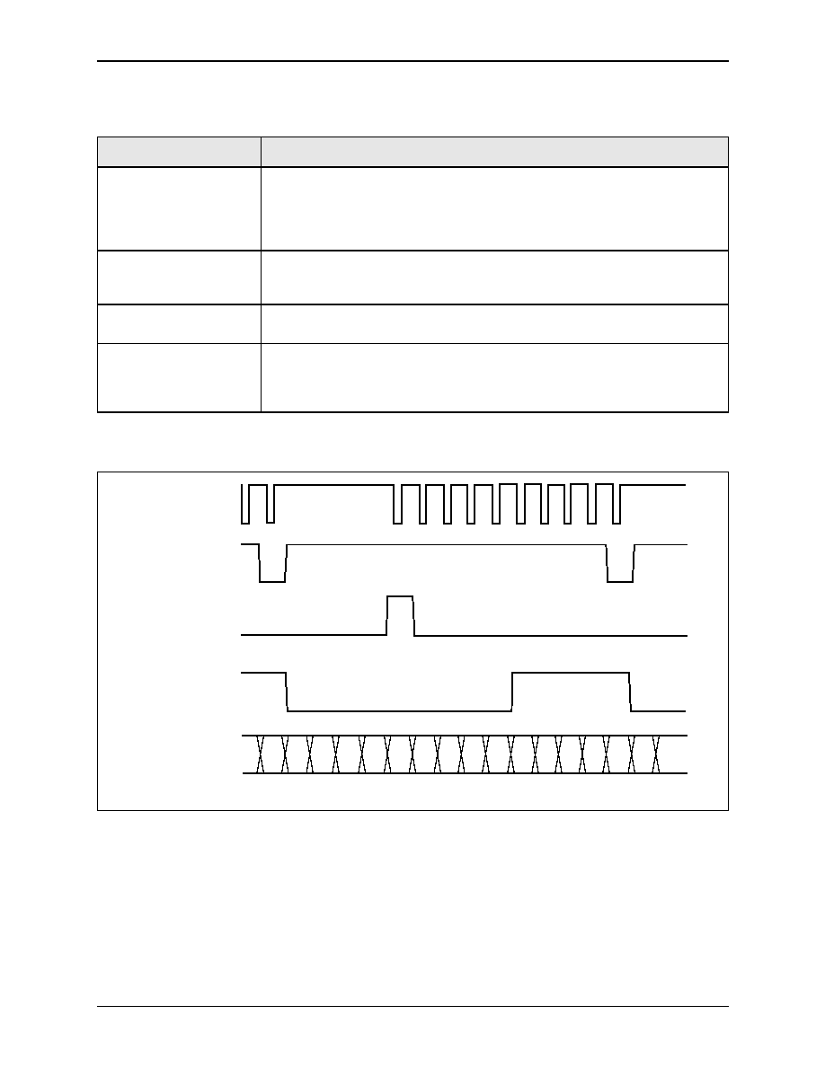
CN8223
2.0 Functional Description
ATM Transmitter/Receiver with UTOPIA Interface
2.7 FIFO Port/UTOPIA Interface
100046C
Conexant
2-39
Table 2-24. FIFO Transmit Pin Functional Descriptions
CN8223 FIFO Pin Function
Functional Description
Transmit Data FIFO Empty
In the transmit direction, the Transmit Data FIFO Empty input inhibits the Transmit Data Read
Strobe for a particular port. The empty flag from the FIFO, when inactive, indicates that the
FIFO contains at least one entire cell of the appropriate length for the selected mode. Data read
strobes to a particular port are inhibited if the empty flag for that port is low. There are four of
these signals, asserted low, one per port.
Transmit PLCP Frame Sync
If using FIFO mode and PLCP mapping, when 57-octet input is selected on the transmitter, the
Transmit PLCP Frame Sync Marker (FCTRL_OUT[16]) is high during the first slot of the PLCP
frame to indicate the start of the frame.
Transmit Start of Cell Marker
In 53-octet mode, FCTRL_OUT[16] indicates the Transmit Start of Cell, informing the FIFO that
the next strobe will read the first octet of the cell to be transmitted.
Transmit Cell Sync Marker
The Transmit Cell Sync Marker is an additional output to delineate cell boundaries to the
transmit data FIFO. This marker is low during the read strobe requesting the last octet of a cell,
and high during all other read strobes regardless of the programmed length of the cell to be
transferred from the FIFO.
Figure 2-17. Receive FIFO Port Interface Timing, 53-Octet Mode
Port X Receive
56
∑∑∑
56
55
1
2
3
4
Data Write Strobe
Receive Cell
Sync Marker
Receive Start-
of-Cell Marker
Receive Cell
Invalid Indication
Receive Data Octet
8223_029
0
0

2.0 Functional Description
CN8223
2.7 FIFO Port/UTOPIA Interface
ATM Transmitter/Receiver with UTOPIA Interface
2-40
Conexant
100046C
2.7.2 Transmit Port Priority Mechanism
Each of the four transmit data read ports has a priority level that is programmable
to four levels. The control bits for setting the port priority level are in the
CELL_GEN_x control registers. Priority level 0 is the highest priority, priority
level 3 is the lowest (see
Table 2-26
).
If more than one port is assigned the same priority level, then arbitration
occurs in port order with bandwidth allocated cyclically to Port 0, Port 1, Port 2,
and Port 3.
The priority state machine looks at the port empty flag inputs for all ports at
priority level 0 and reads cells from these ports cyclically until all port flags
indicate empty. If no cells are available at priority 0, the state machine then looks
at the port empty flags for all ports at priority level 1 and reads cells from these
ports cyclically as long as no priority 0 port has a cell ready.
Table 2-25. FIFO Receive Pin Descriptions
CN8223 FIFO Input
Functional Description
Receive Data Write Strobe
The receive data FIFO interface strobes data octets from FDAT_OUT[8:0] into an external
FIFO device on each rising edge of Receive Data Write Strobe. This strobe is a gated clock
with 48-, 52-, 53-, or 57- strobes for the corresponding number of cell octets, depending
on mode. There are four Receive Data Write Strobes, one per port.
Receive Data FIFO Full
This flag is active low. If Receive Data FIFO Full is asserted by the external FIFO and the
CN8223 attempts a write to that port data, loss occurs. If this happens, Receive FIFO Write
Error pin (FCTRL_OUT[10]) is asserted low. There are four Receive Data FIFO full signals,
one per port.
Receive Cell Sync Marker
The sync marker will be low during the last octet of data transfer and high during all other
octets of the data transfer for each cell regardless of the number of octets selected for
output.
Receive Cell Invalid Indication
This per-port signal indicates that a HEC or other check has failed. The invalid indication will
be low during the first octet of data transfer. If any enabled check fails, the invalid indication
will be high during the last five octets of the cell. If no failures occur, the indication will stay
de-asserted through the end of the cell. The FIFO or a microprocessor must mark this cell
as bad to prevent further processing.
Optional Start of Cell Mode
If Start-of-Cell/Write Error Output [bit 15] in the CELL_VAL register [0x14] is set, then
FCTRL_OUT[10] becomes an active-high start-of-cell output marker for the receiver, and
FCTRL_OUT[16] becomes an active-high start-of-cell output marker for the transmitter.
These indicators are valid only in 53-octet input/output mode. In this mode, the Receive
FIFO Write Error function is not available.
Table 2-26. Priority Levels
CELL_GEN 3
CELL_GEN 2
Priority Level
0
0
0
0
1
1
1
0
2
1
1
3

CN8223
2.0 Functional Description
ATM Transmitter/Receiver with UTOPIA Interface
2.7 FIFO Port/UTOPIA Interface
100046C
Conexant
2-41
If a higher priority port indicates that it has a cell ready during servicing of a
lower priority port, service switches to the higher priority port after completion of
the cell currently being formatted and transmitted. Servicing of ports and priority
levels continues in this manner until the lowest priority ports are serviced and
empty.
Port priority programming is not intended to be dynamic and should be used
only as a configuration setup. Changes in port priority cannot take place until
ports are inactive (via FIFO empty flag or transmit rate shaping).
Unused ports should be programmed to the lowest priority level, and their
empty flag inputs should be connected to ground.
2.7.3 Transmit Rate Shaping Control
Each of the four transmit data ports has a rate shaping control to allow the
allocation of programmable bandwidth to cells originating from this port. The
TX_RATE_01 [0x09] and TX_RATE_23 [0x08] registers control this function.
The transmit circuitry contains a mod-256 master counter to control rate
shaping. This counter is incremented for every ATM cell that is transmitted, and it
rolls over to 0 when count 255 is reached.
The programmed rate value for a port in the TX_RATE_xx registers
determines the count range for which transmission from that port is allowed. For
instance, if Port 0 is programmed with a rate value of 63, transmission of cells
queued at Port 0 will be allowed for 64 (one more than the programmed value) of
the 256 counts of the master counter.
The transmission is spread over all counts of the counter so that transmission
is not bursty. This gives Port 0 a bandwidth allocation of 25 % of the total
outgoing bandwidth even if all of the other ports are inactive.
This allocation scheme is valid for rate values from 1 to 255 resulting in
allocation ranges from 0.8 % to 100 %. Programming a port's rate value to zero
disables transmissions from that port and causes the transmit circuitry to ignore
FIFO flag indications from that port.
The programmed rate value is an upper bound on the transmission from a
particular port, and the exact ratio may not be achieved if multiple ports are active
at the same time.
2.7.4 Receive Port Addressing
Received cells are routed to each of the four FIFO ports depending on the values
in the Header Value and Header Mask registers. These registers allow a range of
ATM cells to be routed to one of the four FIFO ports. Also, the same ATM cell
can be routed to multiple receive FIFO ports if desired.
The HDR_VALx_12 and HDR_VALx_34 register contents are used to match
incoming ATM cell headers. There are four sets of these registers (x = 0, 1, 2, 3),
one set for each of the four receive FIFO ports. If HDR_VALx_12 and
HDR_VALx_34 are a bitwise match to the incoming cell, then this cell is routed
to the x receive FIFO port.

2.0 Functional Description
CN8223
2.7 FIFO Port/UTOPIA Interface
ATM Transmitter/Receiver with UTOPIA Interface
2-42
Conexant
100046C
2.7.4.1 Header
Screening
The HDR_MSKx_12 and HDR_MSKx_34 registers further qualify the bitwise
values in the Header Value registers. There are four sets of these registers (x = 0,
1, 2, 3), one set for each of the four receive FIFO ports. A bit set to 1 in a Header
Mask register sets the same bit position in the Header Value register to a Don't
Care condition for accepting cell headers.
An example of Header Value and Mask register screening for cells received by
FIFO Port 0 follows:
HDR_VAL0_12 = 0000 H
HDR_VAL0_34 = F000 H
HDR_MSK0_12 = 0000 H
HDR_MSK0_34 = 0000 H
This header screening setup for FIFO Port 0 receives cells with octets 1 2 3 4
equal to 00 00 F0 00. Since the Header Mask bits for Port 0 are all 0, there is no
effect on the header value screening.
In the following example the Header Mask value allows multiple cells to be
accepted by FIFO Port 0:
HDR_VAL0_12 = 0000 H
HDR_VAL0_34 = F000 H
HDR_MSK0_12 = 0000 H
HDR_MSK0_34 = 0003 H
This header screening setup for FIFO Port 0 accepts four different received
cells with octets 1 2 3 4 equal to 00 00 F0 00, 00 00 F0 01, 00 00 F0 02, or 00 00
F0 03. The 2 bits set in HDR_MSK0_12 set Don't Care conditions for the same 2
bit positions in HDR_VAL0_12. This allows four different ATM cell headers to
be accepted by FIFO Port 0.
These control registers enable the CN8223 to be programmed to accept only
certain slot types, or all slots whether busy or not, and also to screen slots for a
particular VCI/VPI pattern. To disable header screening completely, write the
mask register to all 1s. Headers are screened after any error correction is
performed by the HEC circuitry.
2.7.4.2 Output
Screening
The receiver circuitry contains buffer storage so that the header octets can be
examined to determine which, if any, port is to be activated for output. This
allows output of the PLCP and header octets in 57- and 53-octet modes,
respectively.
Header octets are compared to the programmed values in the HDR_VAL
registers under control of the HDR_MSK registers. If a match is made, the data
write strobe for that port is activated, and the cells are written to the port. By
using the mask bits to mark Don't Care locations, cells with different header
values can be sent to a single port. This allows entire VCI/VPI "pages" to be sent
to the same location. Also, several ports can be programmed to receive cells with
the same header values or overlapping pages of header values resulting in a
programmable broadcast capability.
If Accept/Reject [bits 15≠12] in CONFIG_3 [0x02], is set for a particular port,
then all cells with headers matching the programmed header value and mask
criteria are rejected by the port, and all other cells are accepted for output. This
feature can be used to screen certain VCI/VPI values from being output to a
particular port.

CN8223
2.0 Functional Description
ATM Transmitter/Receiver with UTOPIA Interface
2.7 FIFO Port/UTOPIA Interface
100046C
Conexant
2-43
If Delete Idle Cells [bit 2] of CONFIG_4 [0x29] is set, then received cells
matching the idle header and mask criteria are automatically screened from
appearing on the output of all ports.
This idle cell screening is in addition to any reject values that are programmed
for the individual ports. Only addressed ports have active strobes.
2.7.5 UTOPIA Interface
The CN8223 incorporates an interface that is compliant with both the ATM
Forum UTOPIA Level 1 (Version 2.01) Specification and the Saturn Compliant
Interface for ATM PHY Devices Specification.
When the UTOPIA interface is enabled, the CN8223 becomes a single port
device with all input and output of cell data taking place on Port 0.
Configurations for ports 1, 2, and 3 (such as header values and masks or rate
controls) are ignored when in UTOPIA mode. The header values, masks, rate
controls, and other per-port configuration control bits for Port 0 govern the
operation of the UTOPIA port cell stream.
The UTOPIA interface contains transmit and receive buffer FIFOs with a
depth of four cells and is programmable for reduced latency requirements per
ATM Forum document 94/0317. UTOPIA interface pins are listed in
Table 2-27
.
The UTOPIA interface is controlled by
0x2B--UTOPIA_1 (Utopia Port
Control Register 1)
and
0x2C--UTOPIA_2 (Utopia Port Control Register 2)
. The
timing for the UTOPIA interface is functionally compatible with the timing
shown in the Version 2.01 ATM Forum Specification. Detailed timing
information can be found in
Chapter 4.0
.
Table 2-27. UTOPIA Interface Pins
UTOPIA Signal
CN8223 Pin
Signal Direction Relative to
CN8223
TxData (7:0)
FDAT_IN[7:0]
In
TxPrty 0
FDAT_IN[8]
In
TxSOC
FCTRL_IN[0]
In
TxEnb~
FCTRL_IN[1]
In
TxClk
FCTRL_IN[2]
In
TxFull~/TxClav
FCTRL_OUT[2]
Out
RxData (7:0)
FDAT_OUT[7:0]
Out
RxPrty 0
FDAT_OUT[8]
Out
RxSOC
FCTRL_OUT[0]
Out
RxEnb~
FCTRL_IN[3]
In
RxClk
FCTRL_IN[4]
In
RxEmpty~/RxClav
FCTRL_OUT[1]
Out
--
FCTRL_IN[5:7]
Reserved, Connect to Ground
--
FCTRL_OUT[16:4]
Undefined Output
RcvFifoOverflow
FCTRL_OUT[3]
Out

2.0 Functional Description
CN8223
2.8 FEAC Channel and HDLC Data Link Programming
ATM Transmitter/Receiver with UTOPIA Interface
2-44
Conexant
100046C
2.8 FEAC Channel and HDLC Data Link
Programming
This section discusses the use and programming requirements for the FEAC
channel and HDLC data link. The FEAC channel is used in DS3 mode; the
HDLC data link is used by DS3, E3, and STS-1/3 framers.
2.8.1 FEAC Channel Transmitter
The FEAC Channel transmitter is under control of the PHY Type [bits 2≠0],
External Framer [bit 5] of CONFIG_1 [0x00], Transmit Alarm Control [bits 9≠4
of CONFIG_2 [0x01], Enable FEAC Transmission [bit 9], and Transmit FEAC
Data [bits 15≠10] of TXFEAC_ERRPAT [0x03]. An interrupt for use with FEAC
channel operations is available on the DL_INT output pin, and status bits for
determining the interrupt source are located in the RXFEAC_VER register
[0x3C].
The PHY type must be set to internal DS3 for FEAC channel transmission to
take place. In DS3 mode, the last C bit in subframe 1 of the M-frame is used for
transmission. Setting the Transmit Alarm Control [bits 9≠4] for transmission of
AIS disables transmission of the FEAC channel. Transmission of yellow alarm or
idle code has no effect on FEAC channel transmission.
The TXFEAC_ERRPAT register controls the byte to be transmitted on the
FEAC channel. All messages for transmission on the FEAC channel must be in
the form "0xxxmmm011111111". The right-most bit of this sequence is the first
bit transmitted on the channel. To initiate transmission of a message byte in the
FEAC channel, write the desired byte in the form "mmmxxx" into bits 15≠10 of
the TXFEAC_ERRPAT register. A 1 must be written to Enable FEAC
Transmission [bit 9]. Transmission of the flag (11111111) and the 0s on either
side of the "xxxmmm" pattern is automatic. Ten repetitions of the message are
sent before an interrupt is issued on the DL_INT pin. The interrupt also appears
in the RXFEAC_VER register to request a new byte from the processor. To clear
the interrupt, you must write the TXFEAC_ERRPAT register. Each time a new
byte is written, 10 transmissions of that byte (and flag) will automatically occur.
Interrupts from the transmit FEAC channel will occur at a rate of approximately
one interrupt per 17 ms.
If you write a 0 to Enable FEAC Transmission [bit 9], then continuous
transmission of idle flags is enabled and no interrupts are issued until a byte of the
proper format is written to the TXFEAC_ERRPAT register. Interrupts from the
FEAC channel transmitter appear on Transmit FEAC Interrupt [bit 8] in the
RXFEAC_VER register [0x3C].

CN8223
2.0 Functional Description
ATM Transmitter/Receiver with UTOPIA Interface
2.8 FEAC Channel and HDLC Data Link Programming
100046C
Conexant
2-45
2.8.2 FEAC Channel Receiver
The FEAC channel receiver is under control only of the received data stream. The
receiver interrupt is under control of Enable Receive FEAC Interrupt [bit 8] in
TXFEAC_ERRPAT. This interrupt must be enabled by setting this bit for receiver
interrupts to appear on the DL_INT output and for proper interaction with the
processor. The last C bit in subframe 1 in C bit parity mode is provided to the
receiver circuitry at all times.
Receiver status is monitored via Receive FEAC Interrupt [bit 9] in
RXFEAC_VER. When a receive FEAC channel interrupt is generated on
DL_INT, the Receive FEAC Interrupt bit will be set in 0x3C. If this bit is
observed upon reading the RXFEAC_VER, then at least 10 repetitions of the
same byte have been received by the data link and placed in bits 15≠10 of
RXFEAC_VER. The receive interrupt serves as notice that the message bits in
RXFEAC_VER are valid. Reading RXFEAC_VER clears the receive interrupt.
An idle message is all 1s, and all other messages are of the form
"0xxxmmm011111111" with reception of the rightmost bit first from the
channel. The receiver logic recognizes the eight 1s message flag followed by a
message byte and interrupts the controller upon reception of 10 repetitions of a
valid message byte. The "mmmxxx" message byte that was received is stored in
RXFEAC_VER bits 15≠10 at 0x3C. Continuous incoming messages on the
FEAC channel produce an interrupt rate of approximately one interrupt per 17 ms
for this interrupt source. No interrupts are generated if the FEAC channel is
receiving continuous idle flags or if the interrupt is not enabled in
TXFEAC_ERRPAT.
2.8.3 HDLC Data Link Transmitter
The HDLC data link capability is present in the following formats:
∑
DS3 Terminal Data Link C bits
∑
G.751 E3 N bit
∑
G.832 E3 and E4 GC octet
∑
STS-1/STS-3c/STM-1 D1, D2, D3 octet data link
The HDLC formatter has an 8-octet buffer (organized as four 16-bit words)
for both the receiver and transmitter, located at addresses 0x58 through 0x5B and
0x5C through 0x5F, respectively. Addresses are word-wide locations that hold 2
bytes each. Therefore, each buffer has an address range of 4, two for each buffer
half. Each buffer holds 4 octets.
The HDLC data link transmitter is under the control of the Enable HDLC Data
Link [bit 5] in the CONFIG_5 [0x31] and bits 6≠0 in DL_CTRL_STAT [0x60].
An interrupt for use with data link operations is available on the DL_INT output
pin, and status bits for determining the interrupt source are located in
DL_CTRL_STAT.
If the framer is in a mode that allows data link transmission as described
above, the DL_CTRL_STAT register is the main control register used for transmit
data link operations. Disable Data Link Transmission [bit 6] of DL_CTRL_STAT
must be set low to enable operation of the data link. If this bit is set high, an all 1s
signal is transmitted in the data link bit positions in the outgoing serial stream.
With the data link enabled, the Send Message [bit 0], Send FCS [bit 1], and Abort
Message [bit 2] bits of DL_CTRL_STAT control operation. TxBytes[2:0] [bits
5≠3] of DL_CTRL_STAT form a pointer to the TX_DL_BUFFER used by the
data link transmitter.

2.0 Functional Description
CN8223
2.8 FEAC Channel and HDLC Data Link Programming
ATM Transmitter/Receiver with UTOPIA Interface
2-46
Conexant
100046C
The transmitter implements an HDLC data link per ITU standard Q.921. The
functions provided by the data link transmitter circuitry are transparency zero
stuffing, Frame Check Sequence (FCS) generation, idle flag generation, and abort
flag generation. There are no restrictions on the total length of the message.
Q.921 requires that all messages be an integral number of 8-bit bytes. The
transmitter can only transmit 8-bit bytes. The byte transmission times for the
transmitter are approximately those shown in
Table 2-28
.
An 8-byte buffer (organized as four 16-bit words) is provided for the transmit
data link channel to minimize processor interruptions. This buffer is located at
addresses 0x5C through 0x5F. Byte 0 is the least significant byte of 0x5C, byte 1
is the most significant byte of 0x5C, byte 2 is the least significant byte of 0x5D,
etc. Filling of this buffer is accomplished by the processor in the same manner as
writing to control registers. This buffer can be read as well as written to verify
contents. The buffer is divided into two halves to reduce the real-time
requirements on the processor. The processor loads four bytes (2 words) at a time,
while the data link transmitter reads from the other half of the buffer. This gives
the processor at least 160
µs (at the fastest byte rate) to assemble the next four
bytes of message for transmission before the next interrupt is issued. Interrupts
are issued each time the transmitter circuitry reaches a 4-byte buffer boundary.
The transmitter should be initialized with the DL_CTRL_STAT register bits
6≠0 written to zero. This enables the transmitter to send idle flags on the data link.
No interrupts are generated when the data link is sending idle flags, thus no
processor intervention is required until a message is to be sent.
2.8.3.1 Sending a
Message
Beginning with an idle channel, the processor writes the first four bytes of
message data to the TX_DL_BUFFER. The first two bytes of data to be
transmitted should be written to 0x5C. The message is written to the buffer in
ascending order starting at 0x5C and ending at 0x5F. The least significant bit
(LSB) in each byte is transmitted first. This buffer can be written well before the
message is to be sent, if desired. After the first block of data is present in the
buffer memory, the processor writes to the DL_CTRL_STAT register to begin
transmission:
∑
Send Message = 1
∑
TxBytes[2:0] = 3
∑
Send FCS = 0
∑
Abort Message = 0
Table 2-28. Byte Transmission Times for Transmitter
Mode
Byte Transmission Times
DS3 C bit Parity
284
µ
s
G.751 E3
357
µ
s
G.832 E3, E4
125
µ
s
STS-1
125
µ
s
STS-3c/STM-1
42
µ
s

CN8223
2.0 Functional Description
ATM Transmitter/Receiver with UTOPIA Interface
2.8 FEAC Channel and HDLC Data Link Programming
100046C
Conexant
2-47
The 3-bit field TxBytes[2:0] is functionally split into two parts. The most
significant bit (MSB) indicates to the transmitter circuitry which half of the buffer
to read from next. The two LSBs indicate the stop location, i.e., where the last
message byte is located. When the new controls are latched by the transmitter
circuitry, the processor is interrupted for the next set of controls. Now, the
processor has up to 4-byte intervals (byte transmission time periods) to write a
new set of controls to the control register. Because of a race condition, the ISR
that is processing the transmit interrupt must delay 1.5 byte times before writing a
new control register value. The processor can now write the next block of data to
the next half of the message buffer.
When the end of a message is reached, or in the event of a short message, there
may not be exactly 4 bytes remaining. In this case, the processor writes the
remaining data to the message buffer as usual. The processor now must write the
highest location used to the TxBytes[2:0] field in the data link control register.
Send FCS is set to 1. This causes the FCS to be sent after this last block of data.
When this set of controls is latched, the processor is interrupted. At this time a
new message can be sent, or Send Message can be set to 0 to send idle flags. If a
new message is to be sent immediately, the next half of the transmit buffer can be
written, and the data link control register configured accordingly. This results in
only one idle flag being transmitted between messages. If there is no new
message ready, the processor must write Send Message to 0. If this is not done
within 4 byte intervals, undefined data is transmitted.
2.8.3.2 Aborting a
Message
To abort a message in progress, the controller writes Abort Message to 1 in the
data link control register. The transmitter finishes sending the message byte in
progress, then transmits an abort flag (11111110). After writing the abort signal
to the control register, a second write may follow the next interrupt to cause the
transmitter to go to the idle condition or to transmit another message. In the latter
case, the abort flag is followed by one idle flag, and the new message begins. If
the second write is not performed, the formatter continues to transmit abort flags
until instructed otherwise.
2.8.3.3 Transmitter
Interrupts
The transmitter generates an interrupt when it has latched the present set of
controls and is ready for a new set. There are no interrupts during the
transmission of idle flags. Therefore, to start a message from an idle condition,
the processor writes the first half of the buffer and the proper control bits. When
the circuit latches these controls internally, an interrupt is immediately issued for
the next set of control bits. The processor then has up to 4 byte intervals to
respond to the interrupt. The interrupt appears on the DL_INT pin. The
DL_CTRL_STAT register indicates the source of the interrupt but not the cause.
The controller software must know from the message context what response is
required. The interrupt is an active low level, not a pulse. The transmit interrupt is
cleared upon the writing of the DL_CTRL_STAT register. A write operation must
be performed to clear the current interrupt and prevent missing later interrupts.
If the interrupt is a mid-message interrupt, a new data link control word must
be written with TxBytes[2:0] equal to the ending location of the next message
block. The MSB of TxBytes[2:0] informs the transmit circuitry which half of the
buffer to read next.
Interrupts from the HDLC data link transmitter will appear on Transmitter
Interrupt [bit 14] in DL_CTRL_STAT [0x60]. Interrupts must be enabled to
appear on DL_INT by setting Enable HDLC Data Link = 1 in CONFIG_5.

2.0 Functional Description
CN8223
2.8 FEAC Channel and HDLC Data Link Programming
ATM Transmitter/Receiver with UTOPIA Interface
2-48
Conexant
100046C
2.8.3.4 Transmitter
Control Example
This example shows the sequence necessary to transmit a 10-byte hex message
starting in the low half of the transmit buffer. With the transmitter in the idle state,
the processor executes the following sequence:
write bytes 1 and 2 to address 0x5C
write bytes 3 and 4 to address 0x5D
write 19 to address 0x60 (bytes = 3, send message = 1)
at TX Interrupt:
write bytes 5 and 6 to address 0x5E
write bytes 7 and 8 to address 0x5F
write 39 to address 0x60 (bytes = 7, send message = 1)
at TX Interrupt:
write bytes 9 and 10 to address 0x5C
write 0B to address 0x60 (bytes = 1, send message = 1,
send FCS = 1)at TX Interrupt:
write 00 to address 0x60 (send message = 0, send FCS = 0
2.8.4 HDLC Data Link Receiver
The HDLC data link receiver is under the control of the received data stream only.
The receiver interrupt is under the control of Enable Receive Data Link Interrupt
[bit 7] in DL_CTRL_STAT [0x60]. You must enable this interrupt by setting this
bit for receiver interrupts to appear on the DL_INT output and for proper
interaction with the processor. The HDLC data link capability is present in the
following formats:
∑
DS3 Terminal Data Link C bits
∑
G.751 E3 N bit
∑
G.832 E3 and E4 GC octet
∑
STS-1/STS-3c/STM-1 D1, D2, D3 octet data link
The data link bits are provided to the receiver circuitry at all times. Therefore,
when the LINE_STATUS register [0x38] indicates that alarms are being received
that render the data link information useless, you can disable the receive data link
interrupt to prevent excessive or spurious interrupts to the processor. Receiver
status is monitored via Receiver Interrupt [bit 15] in DL_CTRL_STAT and via
the receiver status bits in that register (bits 13-8). When a receive data link
interrupt is generated on DL_INT, the Receiver Interrupt bit is set. If this bit is
observed upon reading the DL_CTRL_STAT register, then the status obtained
from bits 13≠8 indicates the receiver status that caused the interrupt.
The DL_CTRL_STAT register contains three status bits and a three-bit buffer
pointer. The status bits are Abort Flag Received [bit 8], Bad FCS [bit 9], and Idle
Code Received [bit 10]. The 3-bit buffer pointer RxBytes[2:0] [bits 13≠11] is
used to point to locations in the 8-byte (organized as four 16-bit words)
RX_DL_BUFFER. This buffer is located at addresses 0x58 through 0x5B. The
buffer pointer indicates the last location written by the data link receiver. Byte 0
of the buffer is the least significant byte of 0x58, byte 1 is the most significant
byte of 0x58, byte 2 is the least significant byte of 0x59, etc.

CN8223
2.0 Functional Description
ATM Transmitter/Receiver with UTOPIA Interface
2.8 FEAC Channel and HDLC Data Link Programming
100046C
Conexant
2-49
2.8.4.1 Receiver
Operation
The receiver implements an HDLC data link per ITU standard Q.921. The
functions provided by the data link receiver circuitry are transparency-zero
removal, FCS checking, idle flag reception, and abort flag reception. There are no
restrictions on the total length of the message. Q.921 requires that all messages be
an integral number of 8-bit bytes. If the receiver receives a message that is not an
integral number of bytes, the receiver status indicates a message received with
bad FCS. The per-byte reception times are equivalent to those given for the
transmitter for any particular mode.
The receiver powers up in an indeterminate state. It is initialized by the receipt
of an idle flag (0x7E) on the link, which sets Idle Code Received = 1 in the data
link status register (bits 13-8 of 0x60). When the idle flag is removed from the
link and a message starts coming in, the receiver removes stuffed 0s and writes
the resulting data to the receive data link buffer beginning with the least
significant byte of 0x58 and counting up to the most significant byte of 0x5B.
When the first four bytes have been written, the processor is interrupted to
read the data out of the buffer. The processor has 4 byte intervals to read the data
before it is overwritten with new data. The interrupt is cleared when the processor
reads DL_CTRL_STAT. The status register indicates a message in progress at this
time:
∑
Idle Code Received = 0
∑
RxBytes[2:0] = 3
If the upper half of the buffer had just been filled, the status register indicates
RxBytes[2:0] = 7, and locations 4 through 7 must be read during the next 4 byte
intervals to retrieve the message.
When the last block of data has been received, the processor is again
interrupted. This time, the data link status register indicates the end of message:
∑
Idle Code Received = 1
∑
RxBytes[2:0] = n
∑
Bad FCS = 0 or 1
The RxBytes[2:0] = n portion of the register indicates the highest-numbered
location that was written in the receive buffer. Locations 0 to n or 4 to m (where
n = 0 to 3 and m = 4 to 7) must be read to retrieve the data depending on what has
already been read at the previous interrupt. The two highest-numbered locations
contain the FCS that was received at the end of the message. A new incoming
message always starts in the opposite buffer half from where the previous
message ended to prevent overwriting of previously received bytes and allow the
processor time to retrieve those bytes. For example, if a message ended in buffer
0x5A or 0x5B, the next message received would be stored starting in 0x58. If a
message ended in buffer 0x58 or 0x59, the next message received would be stored
starting in 0x5A.
If the received message is a multiple of 8 bytes, then when the processor is
interrupted to read the last block of data, the FCS has yet to be received. In this
event, the processor is again interrupted when the FCS has been checked, and an
idle flag received. The data link status register shows RxBytes[2:0] = 1 (or 5),
FCS good or bad, and Idle Code Received = 1; and the FCS that was received will
be in locations 0 and 1 (or 4 and 5). Again, the data must be read out during the
next 4 byte intervals, or it may be overwritten by a new incoming message.

2.0 Functional Description
CN8223
2.8 FEAC Channel and HDLC Data Link Programming
ATM Transmitter/Receiver with UTOPIA Interface
2-50
Conexant
100046C
Alternatively, the FCS data may be ignored, and the good or bad indication
used directly. It is important that software strategies allow for the fact that the
LAPD receiver cannot recognize the FCS as such until the closing flag is
recognized. It can happen that the processor is interrupted to read 4 message
bytes, and the next byte received is the closing flag.
When the processor exits the interrupt routine, another interrupt will be
pending for the end of message. The status for this interrupt indicates the idle
condition, the FCS status, and the byte count will be the same as the previous
interrupt (RxBytes[2:0] = 3 or 7) because no extra bytes were received. In this
event, the last two bytes read from memory on the previous interrupt were not
message bytes after all, but were actually the FCS bytes. If the FCS spans a 4-byte
boundary, the final interrupt indicates that one additional byte was received
(RxBytes[2:0] = 0 or 4), the idle condition, and the FCS status.
2.8.4.2 Receiver
Interrupts
The data link receiver generates an interrupt in response to three events:
1.
The current half of the message buffer is full
2.
The end-of-message flag was detected
3.
An abort flag was detected
DL_CTRL_STAT indicates the cause of the interrupt. The interrupt is cleared
upon the reading of this register.
If the interrupt is due to the current half of the receive buffer being full, Idle
Code Received is cleared, and RxBytes[2:0] indicates which half of the buffer
must be read.
If the interrupt is due to the end-of-message flag being detected, Idle Code
Received is set, Bad FCS indicates the result of the FCS error check, and
RxBytes[2:0] indicates the last location written. The processor is not interrupted
again until four bytes of a new message have been received.
If the interrupt is due to an abort flag being received, Abort Flag Received is
set, and there is nothing to be done by software other than discard any previously
received message bytes. The processor will not be interrupted again until four
bytes of a new message have been received.
Interrupts from the HDLC data link receiver appear on Receiver Interrupt
[bit 15] in DL_CTRL_STAT. Interrupts must be enabled to appear on DL_INT by
setting Enable Receive Data Link Interrupt [bit 7] in DL_CTRL_STAT.

CN8223
2.0 Functional Description
ATM Transmitter/Receiver with UTOPIA Interface
2.8 FEAC Channel and HDLC Data Link Programming
100046C
Conexant
2-51
2.8.5 Receiver Response Example
The following example shows the sequence necessary to receive an 8-byte hex
message that was stored starting in the low half of the receive buffer. In this
example, the final interrupt indicates that two more bytes are present in the
buffer; however, these bytes are FCS bytes, not message bytes.
When an interrupt is received, the processor reads DL_CTRL_STAT [0x60] to
determine the source of the interrupt. If the source is determined to be the receive
HDLC data link, the processor responds in the following manner (the status
shown below ignores bits 15 and 14 in DL_CTRL_STAT):
at RX Interrupt:
read address 0x60 to get status (status = 18xx:
bytes = 3, idle = 0)
read address 0x58 to get 1st and 2nd data bytes
read address 0x59 to get 3rd and 4th data bytes at RX
Interrupt:
read address 0x60 to get status (status = 38xx:
bytes = 7, idle = 0)
read address 0x5A to get 5th and 6th data bytes
read address 0x5B to get 7th and 8th data bytes at RX
Interrupt:
read address 0x60 to get status(status = 0Cxx or 0Exx
bytes = 1, idle = 1, bad fcs = 0 or 1)
read address 0x58 if desired (FCS bytes 1 and 2)

2.0 Functional Description
CN8223
2.8 FEAC Channel and HDLC Data Link Programming
ATM Transmitter/Receiver with UTOPIA Interface
2-52
Conexant
100046C

100046C
Conexant
3-1
3
3.0 Registers
3.1 Registers Overview
Table 3-1
displays an overview of the CN8223 registers. All registers are 16-bit, and the addresses are on 16-bit
boundaries. There are seven address pins, A[7:1]. A[0] is always 0; therefore, it does not require a pin.
Table 3-1. ATM Transmitter/Receiver Status Registers, Counters, and Data Link Control
CN8223 Control and Status Registers
Address
Name
Allowed Operations
0x00≠0x31, 0x60
Control Registers
Read and Write
0x38≠0x3B
Status Registers
Read Only
0x3C
Part Number/Version/FEAC Rx
Read Only
0x40≠0x48
Line Framer/PHY Error Counters
Read Only
0x49≠0x4D
Cell Error Counters
Read Only
0x4E≠0x57
Cell Transmitted/Received Counters
Read Only
0x58≠0x5B
Receive HDLC Data Link Buffers
Read Only
0x5C≠0x5F
Transmit HDLC Data Link Buffers
Read and Write

3.0 Registers
CN8223
3.2 Control Register Overview
ATM Transmitter/Receiver with UTOPIA Interface
3-2
Conexant
100046C
3.2 Control Register Overview
Table 3-2
lists the 52 control registers of the CN8223. Control registers are realized as latches within the
CN8223 and are programmed by a write operation from the microprocessor. No initialization is provided for
operational purposes. All registers must be initialized as required for each application by the microprocessor. A
reset signal on the RESET pin (pin 118) resets counters and framer state machines. RESET does not affect
control register contents.
Control bits that do not have a defined function are reserved and must be written to 0. All control registers
can be read to verify contents, except those control bits whose functions cause single events and are, therefore,
not latched.
Control registers in this section have been ordered by function: 7 control configurations, 19 control
transmitter functions, 22 control receiver functions, and 4 enable interrupts.
Table 3-2. ATM Transmitter/Receiver Microprocessor Control Registers (1 of 2)
Address
Name
Function
0x00
CONFIG_1
Configuration Control Register 1
0x01
CONFIG_2
Configuration Control Register 2
0x02
CONFIG_3
Configuration Control Register 3
0x03
TXFEAC_ERRPAT
Transmit FEAC/BIP-8 Error Pattern
0x04
CELL_GEN_0
Cell Generation Control - Port 0
0x05
CELL_GEN_1
Cell Generation Control - Port 1
0x06
CELL_GEN_2
Cell Generation Control - Port 2
0x07
CELL_GEN_3
Cell Generation Control - Port 3
0x08
TX_RATE_23
Transmit Rate Control Value - Ports 2, 3
0x09
TX_RATE_01
Transmit Rate Control Value - Ports 0, 1
0x0A
TX_IDLE_12
Transmit Idle Header Value - Octets 1, 2
0x0B
TX_IDLE_34
Transmit Idle Header Value - Octets 3, 4
0x0C
TX_HDR0_12
Transmit Port 0 Header Value - Octets 1, 2
0x0D
TX_HDR0_34
Transmit Port 0 Header Value - Octets 3, 4
0x0E
TX_HDR1_12
Transmit Port 1 Header Value - Octets 1, 2
0x0F
TX_HDR1_34
Transmit Port 1 Header Value - Octets 3, 4
0x10
TX_HDR2_12
Transmit Port 2 Header Value - Octets 1, 2
0x11
TX_HDR2_34
Transmit Port 2 Header Value - Octets 3, 4
0x12
TX_HDR3_12
Transmit Port 3 Header Value - Octets 1, 2
0x13
TX_HDR3_34
Transmit Port 3 Header Value - Octets 3, 4
0x14
CELL_VAL
Cell Validation Control
0x15
HDR_VAL0_12
Receive Port 0 Header Value - Octets 1, 2

CN8223
3.0 Registers
ATM Transmitter/Receiver with UTOPIA Interface
3.2 Control Register Overview
100046C
Conexant
3-3
0x16
HDR_VAL0_34
Receive Port 0 Header Value - Octets 3, 4
0x17
HDR_VAL1_12
Receive Port 1 Header Value - Octets 1, 2
0x18
HDR_VAL1_34
Receive Port 1 Header Value - Octets 3, 4
0x19
HDR_VAL2_12
Receive Port 2 Header Value - Octets 1, 2
0x1A
HDR_VAL2_34
Receive Port 2 Header Value - Octets 3, 4
0x1B
HDR_VAL3_12
Receive Port 3 Header Value - Octets 1, 2
0x1C
HDR_VAL3_34
Receive Port 3 Header Value - Octets 3, 4
0x1D
HDR_MSK0_12
Receive Port 0 Header Mask - Octets 1, 2
0x1E
HDR_MSK0_34
Receive Port 0 Header Mask - Octets 3, 4
0x1F
HDR_MSK1_12
Receive Port 1 Header Mask - Octets 1, 2
0x20
HDR_MSK1_34
Receive Port 1 Header Mask - Octets 3, 4
0x21
HDR_MSK2_12
Receive Port 2 Header Mask - Octets 1, 2
0x22
HDR_MSK2_34
Receive Port 2 Header Mask - Octets 3, 4
0x23
HDR_MSK3_12
Receive Port 3 Header Mask - Octets 1, 2
0x24
HDR_MSK3_34
Receive Port 3 Header Mask - Octets 3, 4
0x25
RX_IDLE_12
Receive Idle Header Value - Octets 1, 2
0x26
RX_IDLE_34
Receive Idle Header Value - Octets 3, 4
0x27
IDLE_MSK_12
Receive Idle Header Mask - Octets 1, 2
0x28
IDLE_MSK_34
Receive Idle Header Mask - Octets 3, 4
0x29
CONFIG_4
Configuration Control Register 4
0x2A
IDLE_PAY
Transmit Idle Cell Payload Value
0x2B
UTOPIA_1
Utopia Port Control Register 1
0x2C
UTOPIA_2
Utopia Port Control Register 2
0x2D
EN_LINE_INT
Line/PHY Status Interrupt Enable Register
0x2E
EN_EVENT_INT
Status Event Interrupt Enable Register
0x2F
EN_OVFL_INT
Counter Overflow Interrupt Enable Register
0x30
EN_CELL_INT
Cell Counter Interrupt Enable Register
0x31
CONFIG_5
Configuration Control Register 5
0x32
TX_K1K2
Transmit K1, K2 Value for SONET APS
0x33
RX_K1K2
Receive K1, K2 Value for SONET APS
0x60
DL_CTRL_STAT
HDLC Data Link Control and Status Register
Table 3-2. ATM Transmitter/Receiver Microprocessor Control Registers (2 of 2)
Address
Name
Function

3.0 Registers
CN8223
3.3 Configuration Control Registers
ATM Transmitter/Receiver with UTOPIA Interface
3-4
Conexant
100046C
3.3 Configuration Control Registers
0x00--CONFIG_1 (Configuration Control Register 1)
The CONFIG_1 register is located at address 0x00. This register sets chip parameters for both transmit and
receive operations. The line interface type is set for both transmit and receive by bits 7≠0. Valid combinations of
bits 7≠0 for the line interface type in this register are given in
Table 3-3
.
Bit
Field
Size
Name
Description
15
1
STS-1 Stuffing
Option
Enables an alternate ATM mapping for STS-1 mode. If this bit is set, then 84
columns of the SPE are available for ATM cell octets. If this bit is not set, then all 86
columns of the SPE are available for ATM cell octets.
14
1
Source Loopback
Causes the receiver input to be taken from the transmitter output in all modes; the
transmitter output is unaffected. This function allows the generation of
self-diagnostic routines at system startup to ensure the health of the line/physical
framing process. If an external framer mode is selected, the external framer needs to
continue providing an input to TXSYI when source loopback is enabled. Source
loopback does not work in TAXI mode.
13
1
Enable One-Second
Latching of Line
Counters
Causes status indications in the line/PHY counters (other than LCV) to be latched at
one-second intervals. This interval is determined by successive rising clock edges to
ONESECI. If an alarm condition is present during a one-second interval, it is
available to be read on the successive interval. Otherwise, the status is latched and
held until it is read. If this bit is set and the status word is read twice within a
one-second interval, the second read gives the current state of the status word and
clears it.
12
1
Enable One-Second
Latching of Line
Status
Causes status indications in the LINE_STATUS register to be latched at one-second
intervals. The one-second interval is determined by successive rising clock edges to
ONESECI. If an alarm condition is present during a one-second interval, it is
available to be read on the successive interval. Otherwise, the status is latched and
held until it is read. If this bit is set and the status word is read twice within a
one-second interval, the second read gives the current state of the status word and
clears it.
11
1
External 8 kHz
Timing
Forces the transmit PLCP to be synchronized to an external 8 kHz timing reference
rather than to the received PLCP reference. This control bit is meaningful only in
57-octet DS3 and E3 formats.
10
1
Receiver Hold
Enable
Allows the RCV_HLD input to disable cell processing. Internal cell receiver functions
will operate, but no segments will be accepted by the cell validation state machine or
output on the FIFO ports.
9
1
Enable Cell
Scrambler
Enables the x
43
+ 1 scrambler (required for 53-octet direct mapping) for cell
payload.
8
1
Disable LOCD
Allows cell validation and error counting to continue when cell delineation is lost (via
either PLCP or HEC).

CN8223
3.0 Registers
ATM Transmitter/Receiver with UTOPIA Interface
3.3 Configuration Control Registers
100046C
Conexant
3-5
7
1
Enable HEC
Alignment
Enables cell delineation via the HEC alignment method. This method is for use in any
mode where cells are directly mapped into the physical layer. When this bit is set,
53-octet cells are expected. When this bit is low, 57-octet cells (with PLCP framing
overhead) are expected.
6
1
Enable Parallel
Interface
Selects the parallel interface for input/output. When this bit is low, serial data is
expected; when high, parallel data is expected.
5
1
External Framer
Set if line framing is performed with an external framer. When this bit is low, the
internal framer for the selected mode will be used.
4
1
Disable B3ZS/HDB3
Bypasses the internal encoder/decoder so that NRZ data can be presented directly to
the internal framing functions. For E1 and DS1 in external framer mode, set to 0.
3
1
Unframed Input
Specifies whether the serial stream from an external circuit contains overhead or
only payload. The normal mode is framed mode. Physical layer overhead bits are
located by a synchronization input and are ignored by the PHY framer. In unframed
mode, all line framing bit positions are assumed to be nonexistent.
2≠0
3
PHY Type
Sets the type of line framing and physical processing to be used. PHY modes are
always symmetric; the transmit and receive modes are identical. The PLCPs for DS1
and DS3 are described in TR-TSV-000773; E1 and E3 PLCPs are described in ETSI
draft standards prETS 300 213 and prETS 300 214; E3, DS3, and E4 direct-mapped
modes are described in ITU G.832; and STS-1 and STS-3c formats are described in
TR-NWT-000253.
Bit
Field
Size
Name
Description

3.0 Registers
CN8223
3.3 Configuration Control Registers
ATM Transmitter/Receiver with UTOPIA Interface
3-6
Conexant
100046C
Table 3-3. Valid Combinations of CONFIG_1, Bits 0≠7
Type of Line Input Signal
PHY
Type
Unframed
Input
Disable
B3ZS/
HDB3
External
Framer
Enable
Parallel
Interface
Enable
HEC
Align
DS1
0
0
0
1
0
0
or
1
DS1 (externally gapped 192 bits/frame)
0
1
0
1
0
0
E1
1
0
0
1
0
0 or 1
E1 (externally gapped TS0 and TS16)
1
1
0
1
0
0
DS3, Internal Framer
2
0
0 or 1
0
0
0 or 1
DS3, External Framer
2
0
0
1
0
0 or 1
DS3, External Framer (gapped 84/85 bits)
2
1
0
1
0
0
E3, Internal G.751 Format
3
0
0 or 1
0
0
0
E3, External G.751 Format
3
0
0
1
0
0
E3, External G.751 Format
(gapped 1st 16 bits)
3
1
0
1
0
0
E3, Internal G.832 Format
4
x
0 or 1
0
0
1
E4, Internal G.832 Format
5
x
1
0
0
1
STS-1, Internal Framer
6
x
0 or 1
0
0
1
STS-3c/STM-1, Internal Framer
7
x
1
0
0
1
Parallel or TAXI Interface, 53 Octet Cells
0
x
0
1
1
1
Notes: 1. "x" = Don't Care

CN8223
3.0 Registers
ATM Transmitter/Receiver with UTOPIA Interface
3.3 Configuration Control Registers
100046C
Conexant
3-7
0x01--CONFIG_2 (Configuration Control Register 2)
The CONFIG_2 register is located at address 0x01 and controls transmit formatting and alarm generation.
Table 3-4
defines Alarm Controls for the Line Framing/PHY Formats.
Table 3-5
defines the control bits for
STS-1/STS-3c/STM-1.
Table 3-6
defines the overhead bits for Line Framing/PHY Formats.
Bit
Field
Size
Name
Description
15
1
Enable External
Overhead
Enables all overhead octets to be inserted externally in STS-1/STS-3c/STM-1 and
G.832 E3/E4 modes. If this bit is not set, internal generation of overhead octets is
enabled as described in
Section 2.3
.
14
1
All-Zeros FEBE
Inserts an all-0s value in the FEBE field. The all-0s value provides an indication at
the far end that no BIP-8 errors are being detected. BIP-8 status and error counts
are not affected. This control bit is active in all modes whether the FEBE field is
single- or multi-bit.
13
1
All-1s FEBE
Inserts an all-1s value in the FEBE field of the transmit frame. The all-1s value
notifies the far end that the FEBE function is inhibited. BIP-8 status and error counts
are not affected. This control bit is active in all modes whether the FEBE field is
single- or multi-bit.
12≠10
3
BIP Error Insert
Selects the BIP field that will be errored with the TXFEAC_ERRPAT register
according to the following:
These bits are cleared by the transmitter after the error is inserted in the overhead
field, and can be read as 0 to verify that error insertion has taken place.
9≠4
6
Transmit Alarm
Control
Controls the generation of alarms for 57-octet PLCPs and internal framers. No
alarms are transmitted if all bits in this control field are set to 0. Setting any of these
bits to a 1 causes an alarm to be transmitted according to
Table 3-4
and
Table 3-5
.
For example, in STS-3c mode, setting bit 4 to a 1 will cause the Line AIS alarm to be
transmitted.
3≠0
4
Overhead Control
Selectively disables overhead generation. Standard overhead is generated internally
if all bits in this control field are set to 0. Overhead sources for all PHY modes are
given in
Table 2-8
. When a particular overhead field is set to be disabled, it will be
filled with 0s. Overhead generation is disabled dependent on mode, according to the
data in
Table 3-6
.
Bit 12
Bit 11
Bit 10
BIP Field to be Errored
0
0
0
No errors inserted
0
0
1
B1 field (all modes)
0
1
0
B2 field, bits 23:16 (STS-3c/STM-1 mode only)
0
1
1
B2 field, bits 15:8 (STS-3c/STM-1 mode only)
1
0
0
B2 field, bits 7:0 (STS-1/STS-3c/STM-1 modes)
1
0
1
B3 field (STS-1/STS-3c/STM-1 modes)
1
1
0
No errors inserted
1
1
1
B2 field, all 3 octets (STS-3c/STM-1 mode)

3.0 Registers
CN8223
3.3 Configuration Control Registers
ATM Transmitter/Receiver with UTOPIA Interface
3-8
Conexant
100046C
Table 3-4. Alarm Transmission
Line Framing/PHY Format
Alarm Control 7
Alarm Control 6
Alarm Control 5
Alarm Control 4
53-Octet DS1, E1 Modes
Not Used
Not Used
Not Used
Not Used
57-Octet External (PHY types 0≠3)
G1 Yellow (PLCP)
Not Used
Not Used
Not Used
57-octet Internal DS3 Mode
G1 Yellow (PLCP)
X-Bit Yellow
Idle Code
AIS
57-octet Internal G.751 E3 Mode
G1 Yellow (PLCP)
A-Bit Yellow
Not Used
AIS
E3/E4 G.832 (PHY types 4≠5)
Not Used
MA Timing Marker
MA FERF
AIS
53-octet Internal DS3 mode
Not Used
X-Bit Yellow
Idle code
AIS
Table 3-5. Alarm Transmission--STS≠1/STS≠3c/STM≠1
STS-1/STS-3c/STM-1 (PHY Types 6-7) Alarm
Control Bit
Line AIS
Alarm Control 4
Line FERF
Alarm Control 5
Path Yellow
Alarm Control 6
Path FERF
Alarm Control 7
Path AIS
Alarm Control 8
SPE Unequipped
Alarm Control 9
Table 3-6. Overhead Generation Disable
Line Framing/PHY Format
Overhead Bit 3
Overhead Bit 2
Overhead Bit 1
Overhead Bit 0
57-Octet Modes (PHY types 0≠3)
A1, A2, Pn
B1
C1
Trailer Bits
E3/E4 G.832 (PHY types 4≠5)
A1, A2
EM
MA
Not Used
STS-1/STS-3c/STM-1 (PHY types 6≠7)
A1, A2
B1, B2, B3
H1, H2, H3, H4
C1, C2

CN8223
3.0 Registers
ATM Transmitter/Receiver with UTOPIA Interface
3.3 Configuration Control Registers
100046C
Conexant
3-9
0x02--CONFIG_3 (Configuration Control Register 3)
The CONFIG_ 3 register is located at address 0x02 and controls miscellaneous functions.
Bit
Field
Size
Name
Description
15≠12
4
Accept/Reject
Header≠Port 3≠0
Allows each receive port to be programmed to either accept or reject cells with
headers as specified in the RXHDR registers. When this bit is low, cells with
headers matching the header value (as qualified by the mask value) for the port will
be accepted and written out to the port. When this bit is high, cells with matching
headers (as qualified by the mask value) will be rejected, and all other cells will be
accepted and written out to the port.
11
1
Count Block Errors
Changes the count function of Error Counters 5≠9 [0x44≠0x48]. When this bit is
low, the counters count the actual number of errored bits in the BIP or FEBE octets.
When this bit is high, the counters increment once for each errored BIP or FEBE
block per G.826.
10
1
Reserved
Set to 0.
9
1
Line Loopback
Enables a loopback of the incoming receive data and clock to the transmit data and
clock outputs. The receive data is still processed by the receiver circuitry. Invert TX
Clock Output (bit 7) is functional in this mode to allow inversion of the looped clock
at TCLKO (or TCLKO_HS±). Line Loopback is not functional for TAXI or external
framer modes. Upon a hardware RESET (pin 118), this bit will be cleared (set to 0).
8
1
Invert RX Clock
Sampling
Selects the edge of the receive clock input where the incoming receive data is
sampled. When this bit is low, the incoming data on RXIN (or RXIN_HS±) is
sampled by the falling edge of RXCKI (or RXCKI_HS±). When this bit is high, the
incoming data is sampled on the rising edge. This bit must be set for operation in
TAXI mode.
7
1
Invert TX Clock
Output
Selects the active edge of the transmit clock output when connecting directly to an
external LIU. When this bit is low, the falling edge of TCLKO (or TCLKO_HS±) will be
centered on the relevant data outputs. When this bit is high, the rising edge of
TCLKO (or TCLKO_HS±) will be centered on the data outputs.
6
1
For DS3 and G.751
E3 PLCP modes:
Force Nibble
Stuffing
If this bit is low, 13/14 nibble stuffing is performed in DS3 and G.751 E3 PLCP
modes. Stuffing is performed to synchronize the transmit PLCP with either the
external 8 kHz frame reference or the receive PLCP framer, depending on the setting
of External 8 kHz Timing in the CONFIG_1 register.
If this bit is high, the transmitter PLCP framing is allowed to free-run to an
internally generated 8 k frame rate when no clock is available from the 8 kHz input
or the receive PLCP framer. This bit is ignored in modes that do not perform nibble
stuffing.
6
1
For STS-3c and
STM-1 modes: Tx
Overhead Control
In STS-3c and STM-1 modes, this bit determines whether Transmit Overhead bytes
G1, K2#1, and Z2#3 are input from the Transmit Overhead bus or are internally
generated.
When this bit is set to 0 the following are internally generated:
∑
G1-Path FEBE/RDI--Path FEBE is automatically generated in response to
Path BIP errors.
∑
Path RDI (yellow alarm) is inserted according to CONFIG_5, bits 2 and 3.
∑
K2#1--Line FERF is transmitted by setting CONFIG_2 bit 5 to a 1.
∑
Z2#3--Line FEBE alarm is transmitted automatically in response to Line
BIP errors.
When this bit is set to 1, these bytes are obtained from the external TXOVH bus.
5
1
Parity Odd/Even
Set to 1: odd parity FIFO port generation and checking.
Set to 0: even parity FIFO port generation and checking.

3.0 Registers
CN8223
3.3 Configuration Control Registers
ATM Transmitter/Receiver with UTOPIA Interface
3-10
Conexant
100046C
0x29--CONFIG_4 (Configuration Control Register 4)
The CONFIG_ 4 register is located at address 0x29 and controls miscellaneous functions.
4
1
Check Input Parity
Enables parity checking at the FIFO port inputs. This bit must be enabled for the
input parity error status bits or interrupts to be active.
3
1
Disable Write
Strobes on Invalid
Cells
Inhibits the receive port FIFO write strobes when a cell is determined to be invalid
for use with generic FIFOs.
2
1
Enable DS1 PRS
Generator
Causes the physical layer data content to be replaced by a quasi-random signal
stream. This stream is used for certain transmission tests in DS1 systems.
1
1
HEC Coverage
Determines the calculation range for the HEC. If this bit is low, the HEC is calculated
over header octets 1≠4 for ATM cells. If this bit is high, the HEC is calculated over
header octets 2≠4 for SMDS/802.6 cells.
0
1
Enable HEC Coset
Enables the x
6
+ x
4
+ x
2
+ 1 polynomial to be XOR'ed with the calculated HEC prior
to transmission and prior to error detection/correction if HEC is internally
generated. For TAXI mode, enable HEC Coset must be active.
Bit
Field
Size
Name
Description
Bit
Field
Size
Name
Description
15-12
4
Disable CRC
Check-Ports 3≠0
Disables the payload CRC check on a per-port basis. This disable controls only the
output of cells to the FIFO interface and does not control the counting of payload
CRC errors. (Counts are performed collectively, not per port.)
11-8
4
Disable Length
Check-Ports 3≠0
Disables the payload length check on a per-port basis. This disable controls only the
output of cells to the FIFO interface and does not control the counting of payload
length errors. (Counts are performed collectively, not per port.)
7-4
4
Disable Port
Reception-Ports
3≠0
Disables the output of any received cells on a per-port basis. This disable control is
internally synchronized to cell boundaries so that no partial cells are output on a
port.
3
1
Enable TAXI
Interface
Enables an interface specific to 100 Mbps 4B/5B data transceivers on the parallel
interface port. This interface is detailed in
Section 2.5.1
.
2
1
Delete Idle Cells
Allows the screening of cells matching the receive idle header and mask criteria
from appearing on the outputs of any of the receive ports. When this bit is low, idle
cells are not automatically screened from port output. When this bit is high, idle
cells are screened from output on the receive FIFO port.
1
1
Enable External
Section Trace
Allows the section trace octet (C1) to be inserted externally. When this bit is low, the
C1 octet is generated internally. When this bit is high, the C1 octet is inserted from
the TXOVH input bus.
0
1
STM-1/STS-3c
Pointer
Enables the SS bits to be generated in the AU-4 pointer for STM-1 compatibility.
When this bit is low, an STS-3c H1/H2 pointer is generated by the transmitter (no SS
bits present) and the C2
octet
(1)
has the value 0x13. When this bit is high, an STM-1
AU-4 pointer is generated with the SS bits set to 10.
NOTE(S):
(1)
The C2 octet is the STS Path Signal Label. It is allocated to indicate the content of the STS SPE, including the status of the
mapped payloads.

CN8223
3.0 Registers
ATM Transmitter/Receiver with UTOPIA Interface
3.3 Configuration Control Registers
100046C
Conexant
3-11
0x31--CONFIG_5 (Configuration Control Register 5)
The CONFIG_5 register is located at address 0x31 and controls miscellaneous functions. Bits 3≠0 are control
bits which can be written and read. Bits 10, 9, and 8 are read-only status bits.
Bit
Field
Size
Name
Description
15≠11
5
Reserved
Set to 0.
10
1
Receive G1 Bit 5
Indicates the value of the RDI qualifier bit being received in the G1 octet of the
STS-3c/STM-1 frame. This bit would be used in conjunction with bit 4 in the
LINE_STATUS register [0x38] to determine the type of RDI (Path Yellow) being
received.
9
1
Receive G1 Bit 6
Indicates the value of the RDI qualifier bit being received in the G1 octet of the
STS-3c/STM-1 frame. This bit would be used in conjunction with bit 4 in the
LINE_STATUS register [0x38] to determine the type of RDI (Path Yellow) being
received.
8
1
Receive G1 Bit 7
Indicates the value of the RDI qualifier bit being received in the G1 octet of the
STS-3c/STM-1 frame. This bit would be used in conjunction with bit 4 in the
LINE_STATUS register [0x38] to determine the type of RDI (Path Yellow) being
received.
7
1
Bt8222: Reserved
for Bt8222B and
higher including the
CN8223: Reset
Set to 0.
In Bt8222 revision B and higher, this bit is a software reset. Writing this bit to 1 has
the same affect as high logic level on pin 118, RESET.
6
1
Set G1 X Bits All-1s
Sets the X bits in the G1 octet of the PLCP overhead to all 1s when this bit is high.
When this bit is low, the X bits will be all 0s.
5
1
Enable HDLC Data
Link
Enables the internal HDLC data link receiver and transmitter. Programming for the
HDLC data link is described in
Section 2.8
.
4
1
Reserved
Set to 0.
3
1
Transmit G1 Bit 5
Controls the transmission of the qualified RDI signals in the path status octet (G1) in
SONET/SDH modes. The value written to this bit will be placed in the corresponding
bit of the G1 octet.
2
1
Transmit G1 Bit 6
Controls the transmission of the qualified RDI signals in the path status octet (G1) in
SONET/SDH modes. The value written to this bit will be placed in the corresponding
bit of the G1 octet.
1
1
Enable External
Signal Label
Selects the source for the C2 octet in the path overhead for SONET/SDH formats.
When this bit is low, the C2 octet is internally generated. When this bit is high, the
C2 octet is obtained from the TXOVH inputs.
0
1
Transmit Clock
Select
Selects the clock source for the transmitter circuitry. When this bit is low, the
transmit clock is from the TXCKI or TXCKI_HS± inputs. When this bit is high, the
transmit clock is from the RXCKI or RXCKI_HS± inputs to enable loop timing.

3.0 Registers
CN8223
3.3 Configuration Control Registers
ATM Transmitter/Receiver with UTOPIA Interface
3-12
Conexant
100046C
0x2B--UTOPIA_1 (Utopia Port Control Register 1)
The UTOPIA_1 register is located at address 0x2B and controls operation of the UTOPIA interface. Operation
of the UTOPIA interface is detailed in
Section 2.7.5
.
Bit
Field
Size
Name
Description
15≠7
9
Reserved
Set to 0.
6
1
Reset TX FIFO
Resets the address generators and flags associated with the transmit FIFO when
this bit is set high. This bit should be set high when Enable UTOPIA Interface (bit 0)
is first set high, then written low after ATM and PHY layer initialization is complete.
While the CN8223 is being initialized, its bit should be held low. Before setting this
bit high, the ATM layer UTOPIA interface control lines must be in an inactive state. If
they are not, the CN8223 UTOPIA FIFO pointers could become corrupted. To
conserve power, write this bit high if the UTOPIA interface is not used.
5
1
Reset RX FIFO
Resets the address generators and flags associated with the receive FIFO when this
bit is set high. This bit should be set high when the Enable UTOPIA Interface control
bit is first set high and can then be written low after ATM and PHY layer initialization
is complete. While the CN8223 is being initialized, this bit should be held low.
Before setting this bit high, the ATM layer UTOPIA interface control lines must be in
an inactive state. If they are not, the CN8223 UTOPIA FIFO pointers could become
corrupted. To conserve power, this bit should be written high if the UTOPIA
interface is not used.
4
1
Reserved
Set to 0.
3, 2
2
Flag Threshold
Selects the cell look-ahead level for asserting the TxFull~/TxClav flag to the ATM
layer. The control bits and flag look-ahead are as follows:
1
1
Octet/Cell
Handshake
Selects the full flag handshake protocol for the FIFO buffers. If this bit is low, then
octet-level handshaking is selected and the flags supplied are TxFull~ and
RxEmpty~. If this bit is high, then cell-level handshaking is selected, and the flags
supplied are TxClav and RxClav. In octet-handshake mode, the RxClav flag goes
active after one full cell is in the receive UTOPIA FIFO. Also in this mode, when the
256-byte transmit UTOPIA FIFO has 252 bytes filled, TxClav goes active, indicating
that only four bytes of space remain.
0
1
Enable UTOPIA
Interface
Selects the interface type on the FIFO I/O pins. If this bit is low, the interface is the
standard four-port FIFO interface. If this bit is high, then the interface is a
single-port UTOPIA-compliant interface controlled by the Port 0 Control Registers.
Octet/Cell
Handshake
Flag Threshold
TxFull~/TxClav Look-Ahead
0
x
Full after 4 more octets
1
00 (Two-cell look-ahead)
Full after current cell + 2 cells
1
01 (Single cell look- ahead)
Full after current cell + cell
1
10 or 11 (Normal mode)
Full after current cell

CN8223
3.0 Registers
ATM Transmitter/Receiver with UTOPIA Interface
3.3 Configuration Control Registers
100046C
Conexant
3-13
Use the following steps to initialize the CN8223 for proper UTOPIA port operation:
1.
Put RS8234 in the global reset: write 0x40000000 to CONFIG0.
2.
Write RS8234's CONFIG0 to appropriate values, but do not overwrite the
GLOBAL_RESET bit.
3.
Put CN8223 in the reset mode: write 0x0080 to CONFIG_5.
4.
Initialize CN8223, including UTOPIA interface if needed.
5.
Release CN8223 reset: write 0x0000 to CONFIG_5.
6.
Release RS8234 reset: set GLOBAL_RESET bit to 0.
7.
Enable RS8234's Reassembly coprocessor.
8.
Enable CN8223's Receiver: write 0x0C02 to CELL_VAL register.
9.
Enable RS8234's Segmentation coprocessor.
0x2C--UTOPIA_2 (Utopia Port Control Register 2)
The UTOPIA_2 register is located at address 0x2C and controls operation of the UTOPIA interface.
Bit
Field
Size
Name
Description
15≠6
10
Reserved
Set to 0.
5≠0
6
Reserved
Set to 35 hex.

3.0 Registers
CN8223
3.4 Transmit Control Registers
ATM Transmitter/Receiver with UTOPIA Interface
3-14
Conexant
100046C
3.4 Transmit Control Registers
0x03--TXFEAC_ERRPAT (Transmit FEAC/Error Pattern Register)
The TXFEAC_ERRPAT register is located at address 0x03. The eight MSBs control the FEAC channel used for
DS3. Programming of the FEAC channel is discussed in
Section 2.8
.
The eight LSBs of this register insert BIP-8 errors in the transmitted PLCP, G.832, or SONET overhead or
HEC errors in the cell header for end-to-end testing. The error pattern is XOR'ed with the selected field that is
to be errored.
Bit
Field
Size
Name
Description
15≠10
6
Transmit FEAC Data
Six bits of serial data.
9
1
Enable FEAC
Transmission
Enables FEAC transmission; message is transmitted 10 times. Interrupt on DL_INT
when done.
8
1
Enable Receive
FEAC Interrupt
Turns on the interrupt for the FEAC receive.
7≠0
8
Error Insertion
Pattern
BIP-8 errors for PLCP, G.832, or SONET.

CN8223
3.0 Registers
ATM Transmitter/Receiver with UTOPIA Interface
3.4 Transmit Control Registers
100046C
Conexant
3-15
0x60--DL_CTRL_STAT (HDLC Data Link Control and Status Register)
The DL_CTRL_STAT register is located at address 0x60. The eight LSBs of this register are control bits and
can be read or written. The eight MSBs are status bits and can only be read. Programming of the HDLC data
link is discussed in
Section 2.8
.
Bit
Field
Size
Name
Description
15
1
Receiver Interrupt
Indicates that the receiver needs service. A read to DL_CTRL_STAT clears this
interrupt.
14
1
Transmitter
Interrupt
Indicates that the transmitter needs service. A write to DL_CTRL_STAT clears this
interrupt.
13≠11
3
RX Bytes[2:0]
A 3-bit pointer to the last location written in the receive message buffer by the data
link receiver.
10
1
Idle Code Received
Indicates that an idle flag sequence (0111 1110) was received on the receive data
link.
9
1
Bad FCS
Set when an erroneous Frame Check Sequence (FCS) was received at the end of a
message or an idle flag is received that is not byte aligned.
8
1
Abort Flag Received
Set if an abort sequence (seven consecutive 1s) was received on the receive data
link.
7
1
Enable Receive Data
Link Interrupt
Enables the receiver interrupt to appear on the DL_INT output pin.
6
1
Disable Data Link
Transmission
Forces the data link bits to all 1s.
5≠3
3
TX Bytes[2:0]
A 3-bit pointer to the transmit message buffer indicating the location of the last byte
to be transmitted.
2
1
Abort Message
Causes the data link transmitter to halt the message in progress, send an abort flag,
and then resume transmission of idle flags on the data link.
1
1
Send FCS
Controls the transmission of the FCS at the end of a message block.
0
1
Send Message
Instructs the transmitter to begin transmission of a message block on the data link.
Setting this bit removes the data link from idle flag transmission mode and enables
transmitter interrupts to the controller for data bytes.

3.0 Registers
CN8223
3.4 Transmit Control Registers
ATM Transmitter/Receiver with UTOPIA Interface
3-16
Conexant
100046C
0x04≠0x07--CELL_GEN_x (Cell Generation Control Registers)
The CELL_GEN_x registers are located at addresses 0x04≠0x07. Each of the four FIFO ports has its own ATM
Cell Generation Control Register, so x is 0, 1, 2 or 3. Cell generation is described in detail in
Section 2.6
. A
description of CELL_GEN_x Control Register addresses is provided in
Table 3-7
.
Table 3-7. CELL_GEN_x Control Register Addresses
Address
Register Name
Description
0x04
CELL_GEN_0
Cell Generation Control--Port 0 + UTOPIA
0x05
CELL_GEN_1
Cell Generation Control--Port 1
0x06
CELL_GEN_2
Cell Generation Control--Port 2
0x07
CELL_GEN_3
Cell Generation Control--Port 3
Bit
Field
Size
Name
Description
15, 14
2
Reserved
Set to 0.
13
1
Inhibit Single Cell
Generation
Inhibits cell transmission from the port for a single cell period and inserts an idle
cell in its place.
12
1
Error Payload CRC
Forces an error in the payload CRC-10 field. A single error is generated; then this
bit is cleared.
11
1
Error HEC
Forces an error in the ATM header HEC field. A single error is generated; then this
bit is cleared.
10
1
Disable Payload
CRC
Disables payload CRC-10 field generation and allows the existing field from the
FIFO input to pass.
9
1
Disable HEC
Disables the ATM header HEC field (octet 5) generation and allows the existing field
from the FIFO input to pass. The error mask in the TXFEAC_ERRPAT register
controls which bits are errored in the HEC field by XOR'ing this mask with the
calculated HEC, allowing the microprocessor to generate a specific number of
errors.
8
1
Insert CLP
Performs the same insertion function as Insert GFC (bit 4) for the CLP bit.
7
1
Insert PT
Performs the same insertion function as Insert GFC (bit 4) for the 3-bit payload
type field.
6
1
Insert VCI
Performs the same insertion function as Insert GFC (bit 4) for the 16-bit VCI field.
5
1
Insert VPI
Performs the same function as the Insert GFC (bit 4) for the 8-bit VPI field.
4
1
Insert GFC
Allows the 4-bit GFC field obtained from the FIFO interface to be overwritten with
the value programmed in the corresponding TX_HDR registers [0x0C≠0x13]. This
bit is only valid in 52-, 53-, and 57-octet modes. In 48-octet mode, the GFC field is
always taken from the TX_HDR register.
3, 2
2
Port Priority
Allows the cell generator to assign four priority levels to the transmit source.
1, 0
2
Cell Generation
Mode
Selects the mode of operation for the generation circuit.
0 0 48 octet
0 1 52 octet
1 0 53 octet
1 1 57 octet

CN8223
3.0 Registers
ATM Transmitter/Receiver with UTOPIA Interface
3.4 Transmit Control Registers
100046C
Conexant
3-17
0x08--TX_RATE_23 (Transmit Rate Control Register)
The TX_RATE_23 register is located at address 0x08. Each 8-bit field controls the maximum transmission rate
for ports 3 or 2. These fields are used to control the percentage of the total line rate allocated to each of the four
FIFO transmit ports. Setting these fields to 0 stops transmission on the port. Setting to 0xFF allows the
maximum available rate. Transmit rate control is described in
Section 2.7.3
.
0x09--TX_RATE_01 (Transmit Rate Control Register)
The TX_RATE_01 register is located at address 0x09. Each 8-bit field controls the maximum transmission rate
for ports 1 or 0. These fields are used to control the percentage of the total line rate allocated to each of the four
FIFO transmit ports. Setting these fields to 0 stops transmission on the port. Setting to 0xFF allows the
maximum available rate. Transmit rate control is described in
Section 2.7.3
.
0x0A--TX_IDLE_12 (Transmit Idle Header Register)
The TX_IDLE_12 register is located at address 0x0A. This register sets the ATM idle cell header octets 1 and 2.
0x0B--TX_IDLE_34 (Transmit Idle Header Register)
The TX_IDLE_34 register is located at address 0x0B. This register sets the ATM idle cell header octets 3 and 4.
Bit
Field
Size
Name
Description
15≠8
8
Rate Value-Port 3
Maximum rate: 0x00 to 0xFF
7≠0
8
Rate Value-Port 2
Maximum rate: 0x00 to 0xFF
Bit
Field
Size
Name
Description
15≠8
8
Rate Value-Port 1
Maximum rate: 0x00 to 0xFF
7≠0
8
Rate Value-Port 0
Maximum rate: 0x00 to 0xFF
Bit
Field
Size
Name
Description
15≠8
8
Header Octet 1
Normally written to 00.
7≠0
8
Header Octet 2
Normally written to 00.
Bit
Field
Size
Name
Description
15≠8
8
Header Octet 3
Normally written to 00.
7≠0
8
Header Octet 4
Normally written to 01.
3.0 Registers
CN8223
3.4 Transmit Control Registers
ATM Transmitter/Receiver with UTOPIA Interface
3-18
Conexant
100046C
0x2A--IDLE_PAY (Transmit Idle Cell Payload Register)
The IDLE_PAY register is located at address 0x2A. This register sets the ATM idle cell payload contents.
0x0C≠0x13--TX_HDRx_12, TX_HDRx_34 (Transmit Header Registers)
The Transmit Header registers for port x (where x can be 0 to 3) are located at addresses 0x0C≠0x13. These
registers control the header value that is inserted in cells that are transmitted from port x. Cell generation is
described in detail in
Section 2.6
.
Table 3-8
defines the Tx_HDRx Register addresses.
Bit
Field
Size
Name
Description
15≠9
7
Reserved
Set to 0.
8
1
Enable Idle Cell CRC
Insertion
Allows the CRC-10 value to be calculated and inserted into the last 10 bits of each
transmitted idle cell. Normally written to 0.
7≠0
8
Idle Cell Payload
Octet
Inserted into each of the 48 octets of the information field in all idle cells
transmitted. Normally written to 6A.
Table 3-8. Tx_HDRx Register Addresses
Address
Register Name
Description
0x0C
TX_HDR0_12
Transmit Port 0 ATM Header Value - Octets 1, 2
0x0D
TX_HDR0_34
Transmit Port 0 ATM Header Value - Octets 3, 4
0x0E
TX_HDR1_12
Transmit Port 1 ATM Header Value - Octets 1, 2
0x0F
TX_HDR1_34
Transmit Port 1 ATM Header Value - Octets 3, 4
0x10
TX_HDR2_12
Transmit Port 2 ATM Header Value - Octets 1, 2
0x11
TX_HDR2_34
Transmit Port 2 ATM Header Value - Octets 3, 4
0x12
TX_HDR3_12
Transmit Port 3 ATM Header Value - Octets 1, 2
0x13
TX_HDR3_34
Transmit Port 3 ATM Header Value - Octets 3, 4
Bit
Field
Size
Name
Description
15≠8
8
Header Value--Octet 1
Transmit Port X ATM Header Value--Octet 1
7≠0
8
Header Value--Octet 2
Transmit Port X ATM Header Value--Octet 2
Bit
Field
Size
Name
Description
15≠8
8
Header Value--Octet 3
Transmit Port X ATM Header Value--Octet 3
7≠0
8
Header Value--Octet 4
Transmit Port X ATM Header Value--Octet 4

CN8223
3.0 Registers
ATM Transmitter/Receiver with UTOPIA Interface
3.5 Receive Control Registers
100046C
Conexant
3-19
3.5 Receive Control Registers
0x14--CELL_VAL (Cell Validation Control Register)
The CELL_VAL register is located at address 0x14. Validation checks performed by the validation process can
be individually disabled with the "Disable" control bits. These disable bits are global disables for all ports. Port
disables for payload length and payload CRC checks can also be found in CONFIG_4.
Bit
Field
Size
Name
Description
15
1
Start-of-Cell/Write
Error Output
Selects the function of the FCTRL_OUT[10] pin. When this bit is low, the output
indicates a FIFO write error. When this bit is high, the output is a start-of-cell
marker for the received cell data on the FIFO data port.
14
1
Disable Cell Receiver
Disables all cell validation and output after physical layer reception. This disable
control is internally synchronized to take effect on cell boundaries.
13
1
Enable Status Octet
Enables status output in 53-octet mode on port 3. See
Section 2.6
, for additional
information. When this bit is high, the HEC octet position in the FIFO output data is
omitted and a status word is appended to the end of the cell as octet number 53. In
53-octet cell formats, if status output is enabled with this bit, none of the other
ports should be programmed for 53-octet output.
12
1
Header Only Output
Enables a 5-octet output mode on port 3 only. See
Section 2.6
, for additional
information. Only the 4 header octets of cells addressed to port 3 and the status
octet are output to the FIFO port. In 53-octet cell formats, if status output is
enabled with this bit, none of the other ports should be programmed for 53-octet
output.
11
1
Disable Payload CRC
Disables the payload CRC check. This disable controls only the output of cells to
the FIFO interface and does not control the counting of payload CRC errors. (This
applies for all ports.)
10
1
Disable Payload Len
Disables the payload length check. This disable controls only the output of cells to
the FIFO interface and does not control the counting of payload length errors. (This
applies for all ports.)
9
1
Disable HEC Check
Disables the check of the header error control octet. The CN8223 will pass cells
with HEC errors if this bit is set to 1. This bit is not functional in UTOPIA mode.
8
1
Enable HEC
Correction
Enables the HEC correction mode for single-bit header errors. If this bit is set to 0,
then no correction is performed but error detection is always performed. Error
correction must be disabled if HEC coverage is set for SMDS/802.6 mode or if
Enable HEC Coset (bit 0) in CONFIG_3 is not enabled.
7≠6
2
Cell Output
Mode-Port 3
Number of ATM cell octets delivered to the FIFO interface.
00 - 48 Octets: Payload only mode
01 - 52 Octets: Header + Payload, no HEC
10 - 53 Octets: Header + HEC + payload
11 - 57 Octets: PLCP mode for all table entries

3.0 Registers
CN8223
3.5 Receive Control Registers
ATM Transmitter/Receiver with UTOPIA Interface
3-20
Conexant
100046C
5≠4
2
Cell Output
Mode-Port 2
Number of ATM cell octets delivered to the FIFO interface.
00 - 48 Octets: Payload Only mode
01 - 52 Octets: Header + Payload, no HEC
10 - 53 Octets: Header + HEC + Payload
11 - 57 Octets: PLCP mode
3≠2
2
Cell Output
Mode-Port 1
Number of ATM cell octets delivered to the FIFO interface.
00 - 48 Octets: Payload Only mode
01 - 52 Octets: Header + Payload, no HEC
10 - 53 Octets: Header + HEC + Payload
11 - 57 Octets: PLCP mode
1, 0
2
Cell Output
Mode-Port 0
Number of ATM cell octets delivered to the FIFO interface.
00 - 48 Octets: Payload Only mode
01 - 52 Octets: Header + Payload, no HEC
10 - 53 Octets: Header + HEC + Payload
11 - 57 Octets: PLCP mode
Bit
Field
Size
Name
Description

CN8223
3.0 Registers
ATM Transmitter/Receiver with UTOPIA Interface
3.5 Receive Control Registers
100046C
Conexant
3-21
0x15≠0x1C--HDR_VALx_12, HDR_VALx_34 (Receive Header Value Register)
The Receive Header Value registers for port x (where x can be 0 to 3) are located at addresses 0x15≠0x1C. The
header values direct ATM cells to each port. If an incoming ATM cell header matches the value in the header
register, the cell is directed to that port. Receive Header Mask registers further qualify ATM cell reception.
Table 3-9
defines the HDR_VALx register addresses.
Table 3-9. HDR_VALx Register Addresses
Address
Register Name
Description
0x15
HDR_VAL0_12
Receive Port 0 ATM Header Value--Octets 1, 2
0x16
HDR_VAL0_34
Receive Port 0 ATM Header Value--Octets 3, 4
0x17
HDR_VAL1_12
Receive Port 1 ATM Header Value--Octets 1, 2
0x18
HDR_VAL1_34
Receive Port 1 ATM Header Value--Octets 3, 4
0x19
HDR_VAL2_12
Receive Port 2 ATM Header Value--Octets 1, 2
0x1A
HDR_VAL2_34
Receive Port 2 ATM Header Value--Octets 3, 4
0x1B
HDR_VAL3_12
Receive Port 3 ATM Header Value--Octets 1, 2
0x1C
HDR_VAL3_34
Receive Port 3 ATM Header Value--Octets 3, 4
HDR_VAL0_12, HDR_VAL1_12, HDR_VAL2_12, HDR_VAL3_12
Bit
Field
Size
Name
Description
15≠8
8
Header Value--Octet 1
Receive Port X ATM Header Match Value--Octet 1
7≠0
8
Header Value--Octet 2
Receive Port X ATM Header Match Value--Octet 2
HDR_VAL0_34, HDR_VAL1_34, HDR_VAL2_34, HDR_VAL3_34
Bit
Field
Size
Name
Description
15≠8
8
Header Value--Octet 3
Receive Port X ATM Header Match Value--Octet 3
7≠0
8
Header Value--Octet 4
Receive Port X ATM Header Match Value--Octet 4
3.0 Registers
CN8223
3.5 Receive Control Registers
ATM Transmitter/Receiver with UTOPIA Interface
3-22
Conexant
100046C
0x1D≠0x24--HDR_MSKx_12, HDR_MSKx_34 (Receive Header Mask Register)
The Receive Header Mask registers for port x (where x can be 0 to 3) are located at addresses 0x1D≠0x24.
These registers modify the ATM cell screen in the Receive Header Value register. Setting a bit in the Mask
register causes the corresponding bit in the received ATM cell header to be disregarded for screening. For
example, setting HDR_MSK0_12, bit 0 to 1 causes ATM cells to be accepted to port 0 with either 1 or 0 in the
octet 1, bit 0 position. Combinations of Receive Header Mask bits can select groups of ATM VPI/VCIs for each
of the four ports. The same cells can be sent to more than one port. Setting all bits to 1s overrides the contents of
the Receive Header Value register. HDR_MSKx Register addresses are listed in
Table 3-10
.
Table 3-10. HDR_MSKx Register Addresses
Address
Register Name
Description
0x1D
HDR_MSK0_12
Receive Port 0 ATM Header Mask--Octets 1, 2
0x1E
HDR_MSK0_34
Receive Port 0 ATM Header Mask--Octets 3, 4
0x1F
HDR_MSK1_12
Receive Port 1 ATM Header Mask--Octets 1, 2
0x20
HDR_MSK1_34
Receive Port 1 ATM Header Mask--Octets 3, 4
0x21
HDR_MSK2_12
Receive Port 2 ATM Header Mask--Octets 1, 2
0x22
HDR_MSK2_34
Receive Port 2 ATM Header Mask--Octets 3, 4
0x23
HDR_MSK3_12
Receive Port 3 ATM Header Mask--Octets 1, 2
0x24
HDR_MSK3_34
Receive Port 3 ATM Header Mask--Octets 3, 4
Bit
Field
Size
Name
Description
15≠8
8
Header Value--Octet 1
Receive Port X ATM Header Mask Value--Octet 1
7≠0
8
Header Value--Octet 2
Receive Port X ATM Header Mask Value--Octet 2
HDR_VAL0_34, HDR_VAL1_34, HDR_VAL2_34, HDR_VAL3_34
Bit
Field
Size
Name
Description
15≠8
8
Header Value--Octet 3
Receive Port X ATM Header Mask Value--Octet 3
7≠0
8
Header Value--Octet 4
Receive Port X ATM Header Mask Value--Octet 4

CN8223
3.0 Registers
ATM Transmitter/Receiver with UTOPIA Interface
3.5 Receive Control Registers
100046C
Conexant
3-23
0x25, 0x26--RX_IDLE_12, RX_IDLE_34 (Receive Idle Header Registers)
The Receive Idle Header Value registers are located at addresses 0x25 and 0x26. These registers define ATM
idle cells for the cell receiver. Idle cells are counted and usually discarded.
0x27, 0x28--IDLE_MSK_12, IDLE_MSK_34 (Receive Idle Header Mask Register)
The Receive Idle Header Mask registers are located at addresses 0x27 and 0x28. These registers modify the
ATM cell screen in the RX_IDLE_12, 34 registers. Setting a bit in the Mask register causes the corresponding
bit in the received ATM idle cell header to be disregarded for screening. For example, setting IDLE_MSK_12,
bit 0 to 1, causes cells to be accepted as ATM idle cells with either 1 or 0 in the octet 2, bit 0 position.
Bit
Field
Size
Name
Description
15≠8
8
Header Value--Octet 1
Receive Port X ATM Header Match Value--Octet 1
7≠0
8
Header Value--Octet 2
Receive Port X ATM Header Match Value--Octet 2
Bit
Field
Size
Name
Description
15≠8
8
Header Value--Octet 3
Receive Port X ATM Header Match Value--Octet 3
7≠0
8
Header Value--Octet 4
Receive Port X ATM Header Match Value--Octet 4
Bit
Field
Size
Name
Description
15≠8
8
Header Value--Octet 1
Receive ATM Idle Cell Header Mask Value--Octet 1
7≠0
8
Header Value--Octet 2
Receive ATM Idle Cell Header Mask Valu--Octet 2
Bit
Field
Size
Name
Description
15≠8
8
Header Value--Octet 3
Receive ATM Idle Cell Header Mask Value--Octet 3
7≠0
8
Header Value--Octet 4
Receive ATM Idle Cell Header Mask Value--Octet 4

3.0 Registers
CN8223
3.6 Interrupt Enable Control Registers
ATM Transmitter/Receiver with UTOPIA Interface
3-24
Conexant
100046C
3.6 Interrupt Enable Control Registers
Four registers enable interrupts to appear on the STAT_INT interrupt output pin (pin 64). The EN_LINE_INT
(0x2D), EN_EVENT_INT (0x2E), EN_OVFL_INT (0x2F), and EN_CELL_INT (0x30) enable interrupts based
on the same bit positions in the corresponding STATUS registers. For example, the EN_LINE_INT register
enables the interrupts reported in the LINE_STATUS register.
0x2D--EN_LINE_INT (Enable Line Interrupts)
The EN_LINE_INT register is located at address 0x2D and enables interrupts for the LINE_STATUS register
(0x38). Setting a bit in EN_LINE_INT enables each interrupt condition to appear on STAT_INT.
Bit
Ext. Framer
(57 octet)
Internal DS3
Internal G.751 E3
STS-1/STS-3c/
STM-1
G.832 E3/E4
15
0
0
0
Line FEBE Error
0
14
One Second Count
One Second Count
One Second Count
One Second Count
One Second Count
13
Invalid FEBE
Invalid FEBE
Invalid FEBE
Signal Label
Mismatch
Payload Type
Mismatch
12
FEBE All-1s
FEBE All-1s
FEBE All-1s
Path FERF Error
MA FERF
11
PLCP FEBE Error
PLCP FEBE Error
PLCP FEBE Error
Path FEBE Error
MA FEBE
10
PLCP BIP Error
PLCP BIP Error
PLCP BIP Error
Summary BIP Error
EM BIP Error
9
PLCP Frame Error
PLCP Frame Error
PLCP Frame Error
Line FERF
x
8
PLCP Yellow
PLCP Yellow/LOC
PLCP Yellow
LOC
LOC
7
PLCP LOF 2≠3
PLCP LOF 2≠3
PLCP LOF 2≠3
STS LOF 2≠3
E3/E4 LOF 2≠3
6
PLCP LOF
PLCP LOF
PLCP LOF
STS LOF
E3/E4 LOF
5
PLCP OOF
PLCP OOF/LOC
PLCP OOF
STS OOF
E3/E4 OOF
4
x
DS3 X bit Yellow
E3 A bit Yellow
Path Yellow
x
3
x
DS3 Idle Code
x
Path AIS
x
2
x
DS3 AIS
E3 AIS
Line AIS
E3/E4 AIS
1
x
DS3 OOF
E3 OOF
STS LOP
x
0
LOS (Input)
LOS (Input)
LOS (Input)
LOS (Input)
LOS (Input)
NOTE(S):
Notes: 1. EN_LINE_INT and LINE_STATUS have definitions that change with line interface mode.
2. "x" means content should be disregarded.

CN8223
3.0 Registers
ATM Transmitter/Receiver with UTOPIA Interface
3.6 Interrupt Enable Control Registers
100046C
Conexant
3-25
0x2E--EN_EVENT_INT (Enable Event Interrupts)
The EN_EVENT_INT register is located at address 0x2E and enables interrupts for the EVENT_STATUS
register (0x39). Setting a bit in EN_EVENT_INT enables each interrupt condition to appear on STAT_INT.
Bit
Field
Size
Name
Description
15
1
Receiver Hold Input
Interrupt Enable
Indicates that an active-high input was received on the RCV_HLD input pin.
14≠13
4
Reserved
Set to 0.
12
1
APS Interrupt
Enables interrupt when received value of the K1 or K2 byte changes in the
SONET frame.
11
1
Start of Cell Error
Indicates that a Start of Cell Alignment Error was received on the
FCTRL_IN[0] input pin (109).
10
1
Port 3 Input Parity Error
Interrupt Enable
Enables parity error interrupt from FIFO data input port 3. These interrupts
and status bits will be active only if input parity checking is enabled in
CONFIG_3.
9
1
Port 2 Input Parity Error
Interrupt Enable
Enables parity error interrupt from FIFO data input port 2. These interrupts
and status bits will be active only if input parity checking is enabled in
CONFIG_3.
8
1
Port 1 Input Parity Error
Interrupt Enable
Enables parity error interrupt from FIFO data input port 1. These interrupts
and status bits will be active only if input parity checking is enabled in
CONFIG_3.
7
1
Port 0 Input Parity Error
Interrupt Enable
Enables parity error interrupt from FIFO data input port 0. These interrupts
and status bits will be active only if input parity checking is enabled in
CONFIG_3.
6
1
Idle Cells Interrupt Enable
Enables interrupt when header of an incoming cell matches the header value
programmed in the RX_IDLE and IDLE_MSK registers.
5
1
Non-matching Cells
Interrupt Enable
Enables interrupt when the header of an incoming cell does not match any of
the header values programmed in the HDR_VALx and HDR_MSKx registers.
4
1
Non-zero GFC Interrupt
Enable
Enables interrupt when the 4-bit GFC field of an incoming cell header is any
value other than 0000.
3
1
Payload Length Error
Interrupt Enable
Enables interrupt when an error is detected in the 6-bit payload length field of
the cell trailer. This event is meaningful only for AAL3/4 payloads that contain
a payload length.
2
1
Payload CRC Error
Interrupt Enable
Enables interrupt when an error is detected in the 10-bit payload CRC of the
cell trailer. This event is meaningful only for AAL3/4 payloads that contain a
payload CRC.
1
1
HEC Error Not Corrected
Interrupt Enable
Enables interrupt when an uncorrectable error is detected in the HEC octet of
the cell header.
0
1
HEC Error Corrected
Interrupt Enable
Enables interrupt when an error is detected and corrected in the HEC octet of
the cell header.

3.0 Registers
CN8223
3.6 Interrupt Enable Control Registers
ATM Transmitter/Receiver with UTOPIA Interface
3-26
Conexant
100046C
0x2F--EN_OVFL_INT (Enable Overflow Interrupts)
The EN_OVFL_INT register is located at address 0x2F and enables interrupts for the OVFL_STATUS register
(0x3A). Setting a bit in EN_OVFL_INT enables each interrupt condition to appear on STAT_INT.
Bit
Field
Size
Name
Description
15
1
Counter 9 Line/PHY
Counter Interrupt Enable
Enables interrupts when Line/PHY error counter 9 overflows.
14
1
Counter 8 Line/PHY
Counter Interrupt Enable
Enables interrupts when Line/PHY error counter 8 overflows.
13
1
Counter 7 Line/PHY
Counter Interrupt Enable
Enables interrupts when Line/PHY error counter 7 overflows.
12
1
Counter 6 Line/PHY
Counter Interrupt Enable
Enables interrupts when Line/PHY error counter 6 overflows.
11
1
Counter 5 Line/PHY
Counter Interrupt Enable
Enables interrupts when Line/PHY error counter 5 overflows.
10
1
Counter 4 Line/PHY
Counter Interrupt Enable
Enables interrupts when Line/PHY error counter 4 overflows.
9
1
Counter 3 Line/PHY
Counter Interrupt Enable
Enables interrupts when Line/PHY error counter 3 overflows.
8
1
Counter 2 Line/PHY
Counter Interrupt Enable
Enables interrupts when Line/PHY error counter 2 overflows.
7
1
Counter 1 Line/PHY
Counter Interrupt Enable
Enables interrupts when Line/PHY error counter 1 overflows.
6
1
Idle Cell Interrupt Enable
Enables interrupts when the IDLE_CELL_CNT counter overflows.
5
1
Non-matching Cell
Interrupt Enable
Enables interrupts when the NON_MATCH_CNT counter overflows.
4
1
Non-zero GFC Interrupt
Enable
Enables interrupts when the NON_ZERO_GFC counter overflows.
3
1
Payload Length Error
Interrupt Enable
Enables interrupts when the PAY_LEN_ERR counter overflows.
2
1
Payload CRC Error
Interrupt Enable
Enables interrupts when the PAY_CRC_ERR counter overflows.
1
1
HEC Error Not Corrected
Interrupt Enable
Enables interrupts when the UNCOR_HEC_ERR counter overflows.
0
1
HEC Error Corrected
Interrupt Enable
Enables interrupts when the COR_HEC_ERR counter overflows.

CN8223
3.0 Registers
ATM Transmitter/Receiver with UTOPIA Interface
3.6 Interrupt Enable Control Registers
100046C
Conexant
3-27
0x30--EN_CELL_INT (Enable Cell Interrupts)
The EN_CELL_INT register (0x30) enables interrupts for the CELL_STATUS register (0x3B). Setting a bit in
EN_CELL_INT enables each interrupt condition to appear on STAT_INT (pin 64).
0x32--TX_K1K2 (Transmit K1 and K2 Value)
The TX_K1K2 register (0x32) contains the APS Transmit K1 and K2 values.
0x33--RX_K1K2 (Receive K1 and K2 value)
The RS_K1K2 register (0x33) contains the APS Receive K1 and K2 values.
Bit
Field
Size
Name
Description
15
1
Cell Sent Cntr Ovfl≠Port 3
Enables an interrupt if the CELL_SENT_CNT3 counter overflows.
14
1
Cell Sent Cntr Ovfl≠Port 2
Enables an interrupt if the CELL_SENT_CNT2 counter overflows.
13
1
Cell Sent Cntr Ovfl≠Port 1
Enables an interrupt if the CELL_SENT_CNT1 counter overflows.
12
1
Cell Sent Cntr Ovfl≠Port 0
Enables an interrupt if the CELL_SENT_CNT0 counter overflows.
11
1
Cell Rcvd Cntr Ovfl-Port 3
Enables an interrupt if the CELL_RCV_CNT3 counter overflows.
10
1
Cell Rcvd Cntr Ovfl-Port 2
Enables an interrupt if the CELL_RCV_CNT2 counter overflows.
9
1
Cell Rcvd Cntr Ovfl-Port 1
Enable an interrupt if the CELL_RCV_CNT1 counter overflows.
8
1
Cell Rcvd Cntr Ovfl-Port 0
Enables an interrupt if the CELL_RCV_CNT0 counter overflows.
7
1
Cell Rcvd≠Port 3
Enables port 3 header match interrupt.
6
1
Cell Rcvd≠Port 2
Enables port 2 header match interrupt.
5
1
Cell Rcvd≠Port 1
Enables port 1 header match interrupt.
4
1
Cell Rcvd≠Port 0
Enables port 0 header match interrupt.
3
1
Cell Sent≠Port 3
Enables an interrupt when a cell is transmitted from port 3.
2
1
Cell Sent≠Port 2
Enables an interrupt when a cell is transmitted from port 2.
1
1
Cell Sent≠Port 1
Enables an interrupt when a cell is transmitted from port 1.
0
1
Cell Sent≠Port 0
Enables an interrupt when a cell is transmitted from port 0.
Bit
Field
Size
Name
Description
15-8
8
TX_K1
Value to transmit in the K1 byte of the SONET frame.
7-0
8
TX_K2
Value to transmit in the K2 byte of the SONET frame.
Bit
Field
Size
Name
Description
15-8
8
RX_K1
Value of the last K1 byte received in the SONET frame. A change in this value causes
Bit 12 of the EVENT_STATUS register to be set.
7-0
8
RX_K2
Value of the last K2 byte received in the SONET frame. A change in this value causes
Bit 12 of the EVENT_STATUS register to be set.

3.0 Registers
CN8223
3.7 Status Register Overview
ATM Transmitter/Receiver with UTOPIA Interface
3-28
Conexant
100046C
3.7 Status Register Overview
There are four status registers, as defined in
Table 3-11
. Status registers are read-only. Some of the status
registers will be cleared when read, or have separate clear functions. The status indications can interrupt the
microprocessor if the corresponding bit is set in an Interrupt Enable Control register (
Section 3.6
). The interrupt
appears on the STAT_INT pin (pin 64).
Table 3-11. ATM Transmitter/Receiver Status Registers, Counters, and Data Link Control
Address
Name
Function
0x38
LINE_STATUS
Line Framer/PHY Interrupt Status
0x39
EVENT_STATUS
Event Interrupt Status--all bits are event driven
0x3A
OVFL_STATUS
Counter Overflow Interrupt Status--all bits are event driven
0x3B
CELL_STATUS
Cell Counter Interrupt Status--all bits are event driven
0x3C
RXFEAC_VER
Receive FEAC/Part Number/Version Number

CN8223
3.0 Registers
ATM Transmitter/Receiver with UTOPIA Interface
3.7 Status Register Overview
100046C
Conexant
3-29
0x38--LINE_STATUS (Line Framer/PHY Interrupt Status Register)
The LINE_STATUS register is located at address 0x38. Bit definitions for this register depend on the line
interface mode selected. LINE_STATUS indicates alarms, errors, and framing states of the CN8223 line
receivers. For 53-octet formats that use external framers or the parallel input, the only meaningful bit is the LOC
indication (bit 8). LINE_STATUS interrupts appear on STAT_INT, if they are enabled by writing the desired
bits in EN_LINE_INT. LINE_STATUS bits are set regardless of whether interrupts are enabled.
Each LINE_STATUS bit is latched until read and then cleared if the condition is no longer present. If a status
condition clears before the register is read, the status bit will still be held. Current status can be obtained by
reading the register twice in succession. Upper and lower bytes of LINE_STATUS operate differently in regard
to interrupt generation. Upper definitions of LINE_STATUS (bits 15≠9) are events that generate an interrupt
when the event occurs (for example, if Line FERF [bit 9] in STS-3c mode occurs, a single interrupt will be
generated when the Line FERF occurs).
The lower definitions of LINE_STATUS (bits 8≠0) are level-sensitive conditions, meaning interrupts occur
on any change of state. For example, when LOS occurs in STS-3c mode, an interrupt occurs. When LOS goes
away, a second interrupt occurs. The contents of the LINE_STATUS register are the logical OR of the status
event, for instance, OOF and STAT_INT line. In SONET/SDH or G.832 E3/E4 modes, bits 9, 12, and 13 also
become level-sensitive.
Two examples of this are given:
Example 1: If the line is disconnected, the OOF interrupt goes active. Reading the LINE_STATUS
register causes the STAT_INT line (pin 64) to go inactive. Reading the LINE_STATUS
register again continues to show the OOF condition that caused the interrupt. Reconnecting
the line causes another interrupt. Reading the LINE_STATUS register will cause the
STAT_INT line to go inactive and show OOF active. (OOF will show active because the
contents of LINE_STATUS are the logical OR of OOF and the STAT_INT line. See
waveform in
Figure 3-1
.) Reading the LINE_STATUS register again will show OOF
inactive.
Example 2: If the line is disconnected, OOF will again go active. If you reconnect the line before the
LINE_STATUS register is read, the STAT_INT line will go active. Reading the
LINE_STATUS register will show OOF active and cause STAT_INT line to go inactive.
Reading LINE_STATUS register again will show OOF in the inactive state because the line
was reconnected.
Table 3-12
lists STS-1, STS-3c, and STM-1 LINE_STATUS bit definitions.
Figure 3-1. LINE_STATUS and OOF Example
OOF
Contents of the LINE_STATUS register
STAT_INT line
Read LINE_STATUS
Read LINE_STATUS
8223_030

3.0 Registers
CN8223
3.7 Status Register Overview
ATM Transmitter/Receiver with UTOPIA Interface
3-30
Conexant
100046C
Table 3-12. STS-1,STS-3c, STM-1 LINE_STATUS Bit Definitions
Bit
Name
Description
15
Line FEBE Error
Set if any valid non-0 FEBE value (values 1≠24) is detected in the M1 octet of the
STS-1/STS-3c/STM-1 overhead.
14
One-Second Count
Set if the one-second timer input is detected.
13
Signal Label Mismatch
Set if the received value in the C2 octet does not equal 0x13 for seven consecutive frames.
12
Path FERF Error
Set if a value of 9 is detected in the most significant nibble of the G1 octet of the
STS-1/STS-3c/STM-1 overhead.
11
Path FEBE Error
Set if any valid non-0 FEBE value (values 1≠8) is detected in the most significant nibble of
the G1 octet of the STS-1/STS-3c/STM-1 overhead.
10
Summary BIP Error
Set if there is an error in any of the B1, B2, B3 BIP-8, or BIP-24 codes at the receiver.
9
Line FERF
Set if the three LSBs of the K2 octet are set to "110" for five consecutive frames.
8
LOC
Indicates that HEC cell delineation has been lost. Cell delineation is lost if seven consecutive
HEC errors occur at the current cell delineation position.
7
STS LOF 2≠3
Set if STS LOF is high for three consecutive one-second latching signals (rising edge on
ONESECI).
6
STS LOF
Set when STS OOF is active for 24 consecutive SONET frames.
5
STS OOF
Set if four consecutive errored A1/A2 framing patterns are observed. For STS-3c/STM-1, the
pattern observed consists of the third A1 octet and the first A2 octet.
4
Path Yellow
Set if the path yellow bit in the G1 octet is set for 10 consecutive frames. The RDI qualifier
for this alarm can be observed in bits 8 and 9 of the CONFIG_5 register.
3
Path AIS
Set if H1 and H2 octets are all 1s for three consecutive frames.
2
Line AIS
Set if the three LSBs of the K2 octet are set to "111" for five consecutive frames.
1
STS LOP
Set if a valid pointer as defined in TR-NWT-000253 cannot be found in the H1/H2 pointer of
the STS-1/STS-3c/STM-1 frame.
0
LOS (Input)
Set if there is a LOS detected by the RXLOS~ input pin. For STS-3c/STM-1, the only source
of LOS is RXLOS~. Cells will continue to be output on the receive side until LOCD is
detected, which is about 6 or 7 cells. To stop output of cells immediately, connect RXLOS~
to RCV_HLD after inverting.

CN8223
3.0 Registers
ATM Transmitter/Receiver with UTOPIA Interface
3.7 Status Register Overview
100046C
Conexant
3-31
Table 3-13
provides definitions for the DS3 PLCP and Direct Mapping Mode LINE_STATUS bits.
Table 3-13. DS3 PLCP and Direct Mapping Mode LINE_STATUS Bit Definitions
Bit
Name
Description
15
0
Not used
14
One-Second Count
Set if the one-second timer input is detected.
13
PLCP Invalid FEBE
Set if an invalid FEBE is detected (9≠F) in the G1 octet in 57-octet PLCP formats. Not used in
direct mapping mode.
12
PLCP FEBE All-1s
Set if an invalid FEBE = F is detected in the G1 octet in 57-octet PLCP formats. Not used in
direct mapping mode.
11
PLCP FEBE Error
Set if any valid non-0 FEBE value (values 0x1≠0x8) is detected in the G1 octet in 57-octet PLCP
formats. Not used in direct mapping mode.
10
PLCP BIP Error
Set if there is an error in the BIP-8 code (B1 octet) checking in 57-octet PLCP formats. Not
used in Direct Mapping mode.
9
PLCP Frame Error
Set if there is an error in either the A1 or A2 octets of the PLCP frame pattern for 57-octet
PLCP formats. Not used in direct mapping mode.
8
PLCP Yellow/LOC
In PLCP mode, PLCP yellow indicates that the yellow alarm bit in the G1 octet (57-octet
modes) has been active for 10 consecutive PLCP frames. This bit will also be active for
57-octet formats using external framers or the parallel interface.
In Direct Mapping mode, LOC indicates that HEC cell delineation has been lost. Cell
delineation is lost if seven consecutive HEC errors occur at the current cell delineation
position.This bit will be active for 53-octet formats using external framers or the parallel
interface. (This bit is functionally redundant with bit 5 when configured in this mode).
7
PLCP LOF 2≠3
Set if PLCP LOF is high for three consecutive one-second latching signals (rising edge on
ONESECI). Not used in direct mapping mode.
6
PLCP LOF
Set when PLCP OOF is active for eight consecutive PLCP frames. Not used in direct mapping
mode.
5
PLCP OOF/LOC
Set if the PLCP OOF state has been entered for 57-octet PLCP formats. In direct mapping
mode, it indicates that HEC cell delineation has been lost. Cell delineation is lost if seven
consecutive HEC errors occur at the current cell delineation position. (This bit is functionally
redundant with bit 8 when configured in Direct Mapping mode.)
4
DS3 X-bit Yellow
Set if the internal DS3 framer detects both X1 and X2 low in an M-frame.
3
DS3 Idle Code
Indicates that the internal DS3 framer has detected an idle code signal. A DS3 idle code is a
1100... payload with valid framing and parity, equal X bits, and all subframe 3 C bits set to 0.
2
DS3 AIS
Indicates that the internal DS3 framer has detected an AIS. A DS3 AIS is a 1010... payload with
valid framing and parity, equal X bits, and all C bits set to 0.
1
DS3 OOF
Indicates that the internal DS3 framer has lost frame alignment. An OOF condition for DS3
occurs when 3 out of 16 F bits are in error, or 2 out of 3 M-frames contain M bit errors.
Reframe time is typically 1 ms.
0
LOS (Input)
Set if there is a LOS detected by the internal B3ZS/HDB3 decoder, or if the RXLOS~ input pin is
active low. Internal LOS detection is the occurrence of 175
±
75 zeros prior to B3ZS/HDB3
decoding. The RXLOS~ input pin (RXIN[4]) should be tied high unless an external line
interface unit provides an active low LOS indication.

3.0 Registers
CN8223
3.7 Status Register Overview
ATM Transmitter/Receiver with UTOPIA Interface
3-32
Conexant
100046C
Table 3-14
lists definitions for E3 G.832 and E4 G.832 LINE_STATUS bits.
Table 3-14. E3 G.832, E4 G.832 LINE_STATUS Bit Definitions
Bit
Name
Description
15
0
Not used
14
One-Second Count
Set if the one-second timer input is detected.
13
Payload Type
Mismatch
Set if the received value in the payload type bits of the MA octet do not equal 010 for seven
consecutive frames.
12
MA FERF
Set if the FERF bit in the MA octet is high in the G.832 E3/E4 frame format.
11
MA FEBE
Set if the FEBE bit in the MA octet is high in the G.832 E3/E4 frame format.
10
EM BIP Error
Set if there is an error in the BIP-8 code (EM octet) checking.
9
x
Not used
8
LOC
Indicates that HEC cell delineation has been lost. Cell delineation is lost if seven consecutive
HEC errors occur at the current cell delineation position. This bit will also be active for 53-octet
formats using external framers or the parallel interface.
7
E3/E4 LOF 2≠3
Set if E3/E4 LOF is high for three consecutive one-second latching signals (rising edge on
ONESECI).
6
E3/E4 LOF
Set when E3/E4 OOF is active for 24 consecutive frames.
5
E3/E4 OOF
Set if four consecutive errored A1/A2 framing patterns are observed in the G.832 E3/E4
format.
4, 3
x
Not used
2
E3/E4 AIS
Set if an unframed all-1s pattern (less than 0.25% zero content) is detected in the G.832 E3/E4
format.
1
x
Not used
0
LOS (Input)
Set if a LOS is detected by the internal B3ZS/HDB3 decoder, or if the RXLOS~ input pin is
active low. Internal LOS detection is the occurrence of 175
±
75 zeros prior to B3ZS/HDB3
decoding. The RXLOS~ input pin should be tied high unless an external line interface unit
provides an active low LOS indication.
NOTE(S):
"x" = Bit position is undefined and should be ignored.

CN8223
3.0 Registers
ATM Transmitter/Receiver with UTOPIA Interface
3.7 Status Register Overview
100046C
Conexant
3-33
Table 3-15
lists definitions for E3 G.751 LINE_STATUS bits.
Table 3-15. E3 G.751 LINE_STATUS Bit Definitions
Bit
G.751 E3
Description
15
0
Not used
14
One-Second Count
Set if the one-second timer input is detected.
13
Invalid FEBE
Set if an invalid FEBE is detected (9≠F).
12
FEBE All-1s
Set if an invalid FEBE = F is detected.
11
PLCP FEBE Error
Set if any valid non-0 FEBE value (values 0x1≠0x8) is detected in the G1 octet in 57-octet PLCP
formats
10
PLCP BIP Error
Set if there is an error in the BIP-8 code (B1 octet) checking in 57-octet PLCP formats.
9
PLCP Frame Error
Set if there is an error in either the A1 or A2 octets of the PLCP frame pattern for 57-octet PLCP
formats.
8
PLCP Yellow
PLCP yellow indicates that the yellow alarm bit in the G1 octet (57-octet modes) has been
active for 10 consecutive PLCP frames.
7
PLCP LOF 2≠3
Set if PLCP LOF is high for three consecutive one-second latching signals (rising edge on
ONESECI).
6
PLCP LOF
Set when PLCP OOF is active for eight consecutive PLCP frames.
5
PLCP OOF
Set if the PLCP OOF state has been entered for 57-octet PLCP formats.
4
E3 A-bit Yellow
Set if the internal E3 framer detects the A-bit high in a G.751 E3 frame.
3
x
Not used
2
E3 AIS
E3 alarm signal. Indicates an unframed all-1s signal present for two consecutive frames.
Defined in ITU Recommendation G.775.
1
E3 OOF
Out of Frame. Indicates four consecutive incorrect FAS patterns.
0
LOS (Input)
Set if there is a LOS detected by the internal B3ZS/HDB3 decoder or if the RXLOS~ input pin is
active low. Internal LOS detection is the occurrence of 175
±
75 zeros prior to B3ZS/HDB3
decoding. The RXLOS~ input pin should be tied high unless an external line interface unit
provides an active low LOS indication.
NOTE(S):
"x" = Bit position is undefined and should be ignored.

3.0 Registers
CN8223
3.7 Status Register Overview
ATM Transmitter/Receiver with UTOPIA Interface
3-34
Conexant
100046C
Table 3-16
lists definitions for External Framer, 57-Octet Mode, LINE_STATUS bits.
Table 3-16. External Framer, 57-Octet Mode, LINE_STATUS Bit Definitions
Bit
Ext. Framer
(57 octet)
Description
15
0
Not used
14
One Second Count
Set if the one-second timer input is detected.
13
Invalid FEBE
Set if an invalid FEBE is detected (9≠F).
12
FEBE All-1s
Set if an invalid FEBE = F is detected.
11
PLCP FEBE Error
Set if any valid non-0 FEBE value (values 0x1≠0x8) is detected in the G1 octet in 57-octet PLCP
formats
10
PLCP BIP Error
Set if there is an error in the BIP-8 code (B1 octet) checking in 57-octet PLCP formats.
9
PLCP Frame Error
Set if there is an error in either the A1 or A2 octets of the PLCP frame pattern for 57-octet PLCP
formats.
8
PLCP Yellow
PLCP yellow indicates that the yellow alarm bit in the G1 octet (57-octet modes) has been active
for 10 consecutive PLCP frames.
7
PLCP LOF 2≠3
Set if PLCP LOF is high for three consecutive one-second latching signals (rising edge on
ONESECI).
6
PLCP LOF
Set when PLCP OOF is active for eight consecutive PLCP frames.
5
PLCP OOF
Set if the PLCP OOF state has been entered for 57-octet PLCP formats.
4≠1
x
Not used
0
LOS (Input)
Set if there is a LOS detected by the internal B3ZS/HDB3 decoder or if the RXLOS~ input pin is
active low. Internal LOS detection is the occurrence of 175
±
75 zeros prior to B3ZS/HDB3
decoding. The RXLOS~ input pin should be tied high unless an external line interface unit
provides an active low LOS indication.
NOTE(S):
"x" = Bit position is undefined and should be ignored.

CN8223
3.0 Registers
ATM Transmitter/Receiver with UTOPIA Interface
3.7 Status Register Overview
100046C
Conexant
3-35
Table 3-17
lists status indications for all modes.
Table 3-17. Status Indications for All Modes
Bit
STS-1/STS-3
c/STM-1
Internal DS3
G.832 E3/E4
Internal G.751
E3
Ext. Framer
(57 octet)
Ext. Framer
(53 octet)
15
Line FEBE
Error
0
0
0
0
0
14
One-Sec.
Count
One-Second
Count
One-Second
Count
One-Second
Count
One-Second
Count
One-Second
Count
13
Signal Label
Mismatch
Invalid FEBE
Payload Type
Mismatch
Invalid FEBE
Invalid FEBE
Invalid FEBE
12
Path FERF
Error
FEBE All 1s
MA FERF
FEBE All 1s
FEBE All 1s
FEBE All 1s
11
Path FEBE
Error
PLCP FEBE
Error
MA FEBE
PLCP FEBE Error
PLCP FEBE Error
x
10
Summary BIP
Error
PLCP BIP
Error
EM BIP Error
PLCP BIP Error
PLCP BIP Error
x
9
Line FERF
PLCP Frame
Error
x
PLCP Frame
Error
PLCP Frame
Error
x
8
LOC
PLCP
Yellow/LOC
LOC
PLCP Yellow
PLCP Yellow
LOC
7
STS LOF 2≠3
PLCP LOF 2≠3
E3/E4 LOF 2≠3
PLCP LOF 2≠3
PLCP LOF 2≠3
x
6
STS LOF
PLCP LOF
E3/E4 LOF
PLCP LOF
PLCP LOF
x
5
STS OOF
PLCP
OOF/LOC
E3/E4 OOF
PLCP OOF
PLCP OOF
LOC
4
Path Yellow
DS3 X-bit
Yellow
x
E3 A-bit Yellow
x
x
3
Path AIS
DS3 Idle Code
x
x
x
x
2
Line AIS
DS3 AIS
E3/E4 AIS
E3 AIS
x
x
1
STS LOP
DS3 OOF
x
E3 OOF
x
x
0
LOS (Input)
LOS (Input)
LOS (Input)
LOS (Input)
LOS (Input)
LOS (Input)
NOTE(S):
"x" = Bit position is undefined and should be ignored.

3.0 Registers
CN8223
3.7 Status Register Overview
ATM Transmitter/Receiver with UTOPIA Interface
3-36
Conexant
100046C
0x39--EVENT_STATUS (Event Interrupt Status Register)
The EVENT_STATUS register is located at address 0x39 and has receiver status conditions.
Bit
Field
Size
Name
Description
15
1
Receiver Hold Input
Indicates that an active-high input was received on the RCV_HLD input pin.
14≠13
2
Reserved
Set to 0.
12
1
APS Event
Set when the received value of the K1 or K2 byte changes in the SONET frame.
11
1
TxUTOPIA Sync
Error
This error indicates that the transmit UTOPIA SOC from the host interface is out of
sync with the UTOPIA FIFO Pointers.
10
1
FIFO Port 3 Input
Parity Error
FIFO Port 3 parity error. This status bit and associated interrupt will be active only if
input parity checking is enabled in CONFIG_3.
9
1
FIFO Port 2 Input
Parity Error
FIFO Port 2 parity error. This status bit and associated interrupt will be active only if
input parity checking is enabled in CONFIG_3.
8
1
FIFO Port 1 Input
Parity Error
FIFO Port 1 parity error. This status bit and associated interrupt will be active only if
input parity checking is enabled in CONFIG_3.
7
1
FIFO Port 0 Input
Parity Error
FIFO Port 0 parity error. This status bit and associated interrupt will be active only if
input parity checking is enabled in CONFIG_3.
6
1
Idle Cells
Set if the header of an incoming cell matches the header value programmed in the
RX_IDLE and IDLE_MSK registers.
5
1
Non-matching Cells
Set if the header of an incoming cell does not match any of the header values
programmed in the HDR_VALx and HDR_MSKx registers.
4
1
Non-zero GFC
Set if the 4-bit GFC field of an incoming cell header is any value other than 0000.
3
1
Payload Length
Error
Set if an error is detected in the 6-bit payload length field of the cell trailer. This
event is meaningful only for AAL3/4 payloads that contain a payload length.
2
1
Payload CRC Error
Set if an error is detected in the 10-bit payload CRC of the cell trailer. This event is
meaningful only for AAL3/4 payloads that contain a payload CRC.
1
1
HEC Error-Not
Corrected
Set if an uncorrectable error is detected in the HEC octet of the cell header.
0
1
HEC
Error-Corrected
Set if an error is detected and corrected in the HEC octet of the cell header.

CN8223
3.0 Registers
ATM Transmitter/Receiver with UTOPIA Interface
3.7 Status Register Overview
100046C
Conexant
3-37
0x3A--OVFL_STATUS (Counter Overflow Interrupt Status Register)
The OVFL_STATUS register is located at address 0x3A and indicates when particular counters have
overflowed. Error and Event Counters are described in
Section 3.8
.
Bit
Field
Size
Name
Description
15
1
Counter 9 Line/PHY
Set when Line/PHY error counter 9 overflows.
14
1
Counter 8 Line/PHY
Set when Line/PHY error counter 8 overflows.
13
1
Counter 7 Line/PHY
Set when Line/PHY error counter 7 overflows.
12
1
Counter 6 Line/PHY
Set when Line/PHY error counter 6 overflows.
11
1
Counter 5 Line/PHY
Set when Line/PHY error counter 5 overflows.
10
1
Counter 4 Line/PHY
Set when Line/PHY error counter 4 overflows.
9
1
Counter 3 Line/PHY
Set when Line/PHY error counter 3 overflows.
8
1
Counter 2 Line/PHY
Set when Line/PHY error counter 2 overflows.
7
1
Counter 1 Line/PHY
Set when Line/PHY error counter 1 overflows.
6
1
Idle Cell
Set when the IDLE_CELL_CNT counter overflows.
5
1
Non-matching Cells
Set if the NON_MATCH_CNT counter overflows.
4
1
Non-zero GFC
Set if the NON_ZERO_GFC counter overflows.
3
1
Payload Length Error
Set if the PAY_LEN_ERR counter overflows.
2
1
Payload CRC
Set if the PAY_CRC_ERR counter overflows.
1
1
HEC Error≠Not Corrected
Set if the UNCOR_HEC_ERR counter overflows.
0
1
HEC Error≠Corrected
Set if the COR_HEC_ERR counter overflows.

3.0 Registers
CN8223
3.7 Status Register Overview
ATM Transmitter/Receiver with UTOPIA Interface
3-38
Conexant
100046C
0x3B--CELL_STATUS (Interrupt Status Register)
The CELL_STATUS register is located at address 0x3B.
0x3C--RXFEAC_VER (Receive FEAC/Part Number/Version Number Register)
The RXFEAC_VER register is located at address 0x3C. The lower 8 bits have fixed values. Programming of the
FEAC channel and use of these interrupts is discussed in
Section 2.8
.
Bit
Field
Size
Name
Description
15
1
Cell Sent Cntr Ovfl≠Port 3
Set if the CELL_SENT_CNT3 counter overflows.
14
1
Cell Sent Cntr Ovfl≠Port 2
Set if the CELL_SENT_CNT2 counter overflows.
13
1
Cell Sent Cntr Ovfl≠Port 1
Set if the CELL_SENT_CNT1 counter overflows.
12
1
Cell Sent Cntr Ovfl≠Port 0
Set if the CELL_SENT_CNT0 counter overflows.
11
1
Cell Rcvd Cntr Ovfl-Port 3
Set if the CELL_RCV_CNT3 counter overflows.
10
1
Cell Rcvd Cntr Ovfl-Port 2
Set if the CELL_RCV_CNT2 counter overflows.
9
1
Cell Rcvd Cntr Ovfl-Port 1
Set if the CELL_RCV_CNT1 counter overflows.
8
1
Cell Rcvd Cntr Ovfl-Port 0
Set if the CELL_RCV_CNT0 counter overflows.
7
1
Cell Rcvd≠Port 3
Enables port 3 header match interrupt.
6
1
Cell Rcvd≠Port 2
Enables port 2 header match interrupt.
5
1
Cell Rcvd≠Port 1
Enables port 1 header match interrupt.
4
1
Cell Rcvd≠Port 0
Enables port 0 header match interrupt.
3
1
Cell Sent≠Port 3
Set when a cell is transmitted from port 3.
2
1
Cell Sent≠Port 2
Set when a cell is transmitted from port 2.
1
1
Cell Sent≠Port 1
Set when a cell is transmitted from port 1.
0
1
Cell Sent≠Port 0
Set when a cell is transmitted from port 0.
Bit
Field
Size
Name
Description
15≠10
6
Receive FEAC Data
Contains the data received by the FEAC receiver.
9
1
Receive FEAC
Interrupt
Indicates that the interrupt on the DL_INT pin was from the FEAC receiver when the
internal DS3 framer is enabled.
8
1
Transmit FEAC
Interrupt
Indicates that the interrupt on the DL_INT pin was from the FEAC transmitter when
the internal DS3 framer is enabled.
7≠4
4
Part Number
Fixed value is E (1110).
3≠0
4
Version Number
Provides the version number of the part. CN8223 = 1 (0001)

CN8223
3.0 Registers
ATM Transmitter/Receiver with UTOPIA Interface
3.8 Event/Error Counters
100046C
Conexant
3-39
3.8 Event/Error Counters
The 24 counters to count line and interface events or errors are summarized in
Table 3-18
and explained in
Tables 3-20
through
Table 3-24
. The first nine (addresses 0x40≠0x48) provide counts of error events from the
line or PHY framers. The events that are counted depend on the mode of operation and are summarized in
Table 3-19
. The remaining counters provide counts of ATM cell events.
Counters 5≠9 can be programmed to count block errors instead of individual errors for BIP and FEBE status
by setting Count Block Errors (bit 11) in CONFIG_3. This provides support for G.826 performance monitoring.
Register summary cheat sheets are illustrated in
Figures 3-2
and
3-3
.
Table 3-18. Line and Interface Events/Errors Counters
Address
Name
Function
Reference
0x40
LINE_PHY_CNTR 1
Line Framer/PHY Error Counter 1
3.8
0x41
LINE_PHY_CNTR 2
Line Framer/PHY Error Counter 2
3.8
0x42
LINE_PHY_CNTR 3
Line Framer/PHY Error Counter 3
3.8
0x43
LINE_PHY_CNTR 4
Line Framer/PHY Error Counter 4
3.8
0x44
LINE_PHY_CNTR 5
Line Framer/PHY Error Counter 5
3.8
0x45
LINE_PHY_CNTR 6
Line Framer/PHY Error Counter 6
3.8
0x46
LINE_PHY_CNTR 7
Line Framer/PHY Error Counter 7
3.8
0x47
LINE_PHY_CNTR 8
Line Framer/PHY Error Counter 8
3.8
0x48
LINE_PHY_CNTR 9
Line Framer/PHY Error Counter 9
3.8
0x49
COR_HEC_ERR
Count of Corrected HEC Errors
2.6.2.3
0x4A
UNCOR_HEC_ERR
Count of Uncorrected HEC Errors
2.6.2.3
0x4B
PAY_CRC_ERR
Count of Payload CRC Errors
2.6.2.3
0x4C
PAY_LEN_ERR
Count of Payload Length Errors
2.6.2.3
0x4D
NON_ZERO_GFC
Count of Non-zero GFC Fields
2.6.2.3
0x4E
CELL_SENT_CNT0
Count of Cells Transmitted on Port 0
2.6.1.1
0x4F
CELL_SENT_CNT1
Count of Cells Transmitted on Port 1
2.6.1.1
0x50
CELL_SENT_CNT2
Count of Cells Transmitted on Port 2
2.6.1.1
0x51
CELL_SENT_CNT3
Count of Cells Transmitted on Port 3
2.6.1.1
0x52
CELL_RCV_CNT0
Count of Cells Received on Port 0
2.6.2.3
0x53
CELL_RCV_CNT1
Count of Cells Received on Port 1
2.6.2.3
0x54
CELL_RCV_CNT2
Count of Cells Received on Port 2
2.6.2.3
0x55
CELL_RCV_CNT3
Count of Cells Received on Port 3
2.6.2.3
0x56
IDLE_CELL_CNT
Count of Idle Cells Received on all Ports
2.6.2.3
0x57
NON_MATCH_CNT
Count of Active Cells Not Matching Any Port VCI/VPI
2.6.2.3

3.0 Registers
CN8223
3.8 Event/Error Counters
ATM Transmitter/Receiver with UTOPIA Interface
3-40
Conexant
100046C
Table 3-19. Counted Events
Cntr
Ext. Framer
(57 octet)
Internal DS3
Internal G.751 E3
STS-1/STS-3c/STM-1
G.832 E3/E4
1
Not Used
LCV
LCV
LCV
LCV
2
Not Used
Frame Errors
Frame Errors
STS OOF Events
E3/E4 OOF Events
3
Not Used
Parity Errors
Not Used
Not Used
MA FEBE Events
4
LOCD Events
(Parallel interface)
Path Parity Errors
Not Used
LOCD Events
MA FERF Events
5
Not Used
DS3 FEBE Errors
Not Used
B1 BIP Errors
B1 BIP Errors
6
PLCP Frame Error
PLCP Frame Error
PLCP Frame Error
B2 BIP Errors
Not Used
7
PLCP OOF Events
PLCP OOF Events
PLCP OOF Events
B3 BIP Errors
LOCD Events
8
PLCP BIP-8 Errors
PLCP BIP-8 Errors
PLCP BIP-8 Errors
Path FEBE Errors
Not Used
9
PLCP FEBE Errors
PLCP FEBE Errors
PLCP FEBE Errors
Line FEBE Errors
Not Used

CN8223
3.0 Registers
ATM Transmitter/Receiver with UTOPIA Interface
3.8 Event/Error Counters
100046C
Conexant
3-41
Table 3-20. Internal STS-1, STS-3c Event/Error Counters
Address
Counter Name
Function
0x40
LINE_ PHY_CNTR_1
Not used.
0x41
LINE_ PHY_CNTR_2
Counts STS OOF events. Event also appears on LINE_STATUS, bit 5.
0x42
LINE_ PHY_CNTR_3
Not used.
0x43
LINE_ PHY_CNTR_4
Counts Loss of Cell Delineation (LOCD) events. Event also appears on LINE_STATUS,
bit 8.
0x44
LINE_ PHY_CNTR_5
Counts B1 BIP-8 errors in STS-1, STS-3c, or STM-1.
0x45
LINE_ PHY_CNTR_6
Counts B2 BIP-8 errors in STS-1. BIP-24 errors in STS-3c or STM-1.
0x46
LINE_ PHY_CNTR_7
Counts B3 BIP-8 errors in STS-1, STS-3c, or STM-1.
0x47
LINE_ PHY_CNTR_8
Counts path FEBE errors in the G1 octet. Event also appears on LINE_STATUS, bit 11.
0x48
LINE_ PHY_CNTR_9
Counts Line FEBE errors in the Z2 octet. Event also appears on LINE_STATUS, bit 15.
0x49
COR_HEC_ERR
Counts corrected HEC errors. Event also appears on EVENT_STATUS, bit 0.
0x4A
UNCOR_HEC_ERR
Counts uncorrected HEC errors. Event also appears on EVENT_STATUS, bit 1.
0x4B
PAY_CRC_ERR
Counts payload CRC-10 errors, used in AAL3/4. Event also appears on
EVENT_STATUS, bit 2.
0x4C
PAY_LEN_ERR
Counts payload length errors, used in AAL3/4. Event also appears on
EVENT_STATUS, bit 3.
0x4D
NON_ZERO_GFC
Counts ATM cells received with non-zero GFC fields. Event also appears on
EVENT_STATUS, bit 4.
0x4E
CELL_SENT_CNT0
Count of ATM cells sent from FIFO port 0. Event also appears on CELL_STATUS,
bit 0.
0x4F
CELL_SENT_CNT1
Count of ATM cells sent from FIFO port 1. Event also appears on CELL_STATUS,
bit 1.
0x50
CELL_SENT_CNT2
Count of ATM cells sent from FIFO port 2. Event also appears on CELL_STATUS,
bit 2.
0x51
CELL_SENT_CNT3
Count of ATM cells sent from FIFO port 3. Event also appears on CELL_STATUS,
bit 3.
0x52
CELL_RCV_CNT0
Count of ATM cells received on FIFO port 0. Event also appears on CELL_STATUS,
bit 4.
0x53
CELL_RCV_CNT1
Count of ATM cells received on FIFO port 1. Event also appears on CELL_STATUS,
bit 5.
0x54
CELL_RCV_CNT2
Count of ATM cells received on FIFO port 2. Event also appears on CELL_STATUS,
bit 6.
0x55
CELL_RCV_CNT3
Count of ATM cells received on FIFO port 3. Event also appears on CELL_STATUS,
bit 7.
0x56
IDLE_CELL_CNT
Counts ATM cells received that match the idle cell header screens. Event also
appears on EVENT_STATUS, bit 6.
0x57
NON_MATCH_CNT
Counts ATM cells received that do not match any header screens. Event also appears
on EVENT_STATUS, bit 5.

3.0 Registers
CN8223
3.8 Event/Error Counters
ATM Transmitter/Receiver with UTOPIA Interface
3-42
Conexant
100046C
Table 3-21. Internal DS3 PLCP and Direct Mapping Modes Event/Error Counters
Address
Counter Name
Function
0x40
LINE_ PHY_CNTR_1
Line Code Violation (LCV) in B3ZS/HDB3 decoder when enabled. For B3ZS this counts
both bipolar rule violations and occurrences of three or more 0s. For HDB3 this counts
violations according to ITU Recommendation 0.161.
0x41
LINE_ PHY_CNTR_2
Counts F and M-bit errors.
0x42
LINE_ PHY_CNTR_3
Counts P1/P2 parity errors.
0x43
LINE_ PHY_CNTR_4
Counts C bit path parity errors.
0x44
LINE_ PHY_CNTR_5
Counts DS3 FEBE errors.
0x45
LINE_ PHY_CNTR_6
Counts PLCP frame errors if there is an error in either A1 or A2 octets. Event also appears
on LINE_STATUS, bit 9. Not used in Direct Mapping mode.
0x46
LINE_ PHY_CNTR_7
Counts PLCP OOF events in PLCP Mode. Counts LOCD events in Direct Mapping mode.
Event also appears on LINE_STATUS, bit 5. Not used in Direct Mapping mode.
0x47
LINE_ PHY_CNTR_8
Counts PLCP BIP errors. Event also appears on LINE_STATUS, bit 10. Not used in Direct
Mapping mode.
0x48
LINE_ PHY_CNTR_9
Counts PLCP FEBE errors. Event also appears on LINE_STATUS, bit 11. Not used in
Direct Mapping mode.
0x49
COR_HEC_ERR
Counts corrected HEC errors. Event also appears on EVENT_STATUS, bit 0.
0x4A
UNCOR_HEC_ERR
Counts uncorrected HEC errors. Event also appears on EVENT_STATUS, bit 1.
0x4B
PAY_CRC_ERR
Counts payload CRC-10 errors used in AAL3/4. Event also appears on EVENT_STATUS,
bit 2.
0x4C
PAY_LEN_ERR
Counts payload length errors used in AAL3/4. Event also appears on EVENT_STATUS,
bit 3.
0x4D
NON_ZERO_GFC
Counts ATM cells received with non-zero GFC fields. Event also appears on
EVENT_STATUS, bit 4.
0x4E
CELL_SENT_CNT0
Count of ATM cells sent from FIFO port 0. Event also appears on CELL_STATUS, bit 0.
0x4F
CELL_SENT_CNT1
Count of ATM cells sent from FIFO port 1. Event also appears on CELL_STATUS, bit 1.
0x50
CELL_SENT_CNT2
Count of ATM cells sent from FIFO port 2. Event also appears on CELL_STATUS, bit 2.
0x51
CELL_SENT_CNT3
Count of ATM cells sent from FIFO port 3. Event also appears on CELL_STATUS, bit 3.
0x52
CELL_RCV_CNT0
Count of ATM cells received on FIFO port 0. Event also appears on CELL_STATUS, bit 4.
0x53
CELL_RCV_CNT1
Count of ATM cells received on FIFO port 1. Event also appears on CELL_STATUS, bit 5.
0x54
CELL_RCV_CNT2
Count of ATM cells received on FIFO port 2. Event also appears on CELL_STATUS, bit 6.
0x55
CELL_RCV_CNT3
Count of ATM cells received on FIFO port 3. Event also appears on CELL_STATUS, bit 7.
0x56
IDLE_CELL_CNT
Counts ATM cells received that match the idle cell header screens. Event also appears on
EVENT_STATUS, bit 6.
0x57
NON_MATCH_CNT
Counts ATM cells received that do not match any header screens. Event also appears on
EVENT_STATUS, bit 5.

CN8223
3.0 Registers
ATM Transmitter/Receiver with UTOPIA Interface
3.8 Event/Error Counters
100046C
Conexant
3-43
Table 3-22. Internal G.832 E3/E4 Event/Error Counters
Address
Counter Name
Function
0x40
LINE_ PHY_CNTR_1
Line code violation in B3ZS/HDB3 decoder when enabled. For B3ZS this counts both
bipolar rule violations and occurrences of three or more 0s. For HDB3 this counts
violations according to ITU Recommendation 0.161.
0x41
LINE_PHY_CNTR_ 2
Counts E3/E4 OOF errors. Event also appears on LINE_STATUS, bit 5.
0x42
LINE_ PHY_CNTR_3
Counts MA FEBE events. Event also appears on LINE_STATUS, bit 11.
0x43
LINE_ PHY_CNTR_4
Counts MA FERF events. Event also appears on LINE_STATUS, bit 12.
0x44
LINE_ PHY_CNTR_5
Counts EM BIP-8 errors. Event also appears on LINE_STATUS, bit 10.
0x45
LINE_ PHY_CNTR_6
Not used.
0x46
LINE_ PHY_CNTR_7
Counts LOCD events. Event also appears on LINE_STATUS, bit 8.
0x47
LINE_ PHY_CNTR_8
Not used.
0x48
LINE_ PHY_CNTR_9
Not used.
0x49
COR_HEC_ERR
Counts corrected HEC errors. Event also appears on EVENT_STATUS, bit 0.
0x4A
UNCOR_HEC_ERR
Counts uncorrected HEC errors. Event also appears on EVENT_STATUS, bit 1.
0x4B
PAY_CRC_ERR
Counts payload CRC-10 errors, used in AAL3/4. Event also appears on EVENT_STATUS,
bit 2.
0x4C
PAY_LEN_ERR
Counts payload length errors, used in AAL3/4. Event also appears on EVENT_STATUS,
bit 3.
0x4D
NON_ZERO_GFC
Counts ATM cells received with non-zero GFC fields. Event also appears on
EVENT_STATUS, bit 4.
0x4E
CELL_SENT_CNT0
Count of ATM cells sent from FIFO port 0. Event also appears on CELL_STATUS, bit 0.
0x4F
CELL_SENT_CNT1
Count of ATM cells sent from FIFO port 1. Event also appears on CELL_STATUS, bit 1.
0x50
CELL_SENT_CNT2
Count of ATM cells sent from FIFO port 2. Event also appears on CELL_STATUS, bit 2.
0x51
CELL_SENT_CNT3
Count of ATM cells sent from FIFO port 3. Event also appears on CELL_STATUS, bit 3.
0x52
CELL_RCV_CNT0
Count of ATM cells received on FIFO port 0. Event also appears on CELL_STATUS, bit 4.
0x53
CELL_RCV_CNT1
Count of ATM cells received on FIFO port 1. Event also appears on CELL_STATUS, bit 5.
0x54
CELL_RCV_CNT2
Count of ATM cells received on FIFO port 2. Event also appears on CELL_STATUS, bit 6.
0x55
CELL_RCV_CNT3
Count of ATM cells received on FIFO port 3. Event also appears on CELL_STATUS, bit 7.
0x56
IDLE_CELL_CNT
Counts ATM cells received that match the idle cell header screens. Event also appears on
EVENT_STATUS, bit 6.
0x57
NON_MATCH_CNT
Counts ATM cells received that do not match any header screens. Event also appears on
EVENT_STATUS, bit 5.

3.0 Registers
CN8223
3.8 Event/Error Counters
ATM Transmitter/Receiver with UTOPIA Interface
3-44
Conexant
100046C
Table 3-23. Internal G.751 E3 Event/Error Counters
Address
Counter Name
Function
0x40
LINE_ PHY_CNTR_1
Line code violation in B3ZS/HDB3 decoder when enabled. For B3ZS this counts both
bipolar rule violations and occurrences of three or more 0s. For HDB3 this counts
violations according to ITU Recommendation 0.161.
0x41
LINE_ PHY_CNTR_2
Counts errored FAS patterns.
0x42
LINE_ PHY_CNTR_3
Not used.
0x43
LINE_ PHY_CNTR_4
Not used.
0x44
LINE_ PHY_CNTR_5
Not used.
0x45
LINE_ PHY_CNTR_6
Counts PLCP Frame Errors if there is an error in either A1 or A2 octets. Event also
appears on LINE_STATUS, bit 9.
0x46
LINE_ PHY_CNTR_7
Counts PLCP OOF events. Event also appears on LINE_STATUS, bit 5.
0x47
LINE_ PHY_CNTR_8
Counts PLCP BIP errors. Event also appears on LINE_STATUS, bit 10.
0x48
LINE_ PHY_CNTR_9
Counts PLCP FEBE errors. Event also appears on LINE_STATUS, bit 11.
0x49
COR_HEC_ERR
Counts corrected HEC errors. Event also appears on EVENT_STATUS, bit 0.
0x4A
UNCOR_HEC_ERR
Counts uncorrected HEC errors. Event also appears on EVENT_STATUS, bit 1.
0x4B
PAY_CRC_ERR
Counts payload CRC-10 errors, used in AAL3/4. Event also appears on EVENT_STATUS,
bit 2.
0x4C
PAY_LEN_ERR
Counts payload length errors, used in AAL3/4. Event also appears on EVENT_STATUS,
bit 3.
0x4D
NON_ZERO_GFC
Counts ATM cells received with non-zero GFC fields. Event also appears on
EVENT_STATUS, bit 4.
0x4E
CELL_SENT_CNT0
Number of ATM cells sent from FIFO port 0.
0x4F
CELL_SENT_CNT1
Number of ATM cells sent from FIFO port 1.
0x50
CELL_SENT_CNT2
Number of ATM cells sent from FIFO port 2.
0x51
CELL_SENT_CNT3
Number of ATM cells sent from FIFO port 3.
0x52
CELL_RCV_CNT0
Number of ATM cells received on FIFO port 0.
0x53
CELL_RCV_CNT1
Number of ATM cells received on FIFO port 1.
0x54
CELL_RCV_CNT2
Number of ATM cells received on FIFO port 2.
0x55
CELL_RCV_CNT3
Number of ATM cells received on FIFO port 3.
0x56
IDLE_CELL_CNT
Counts ATM cells received that match the idle cell header screens. Event also appears
on EVENT_STATUS, bit 6.
0x57
NON_MATCH_CNT
Counts ATM cells received that do not match any header screens. Event also appears on
EVENT_STATUS, bit 5.

CN8223
3.0 Registers
ATM Transmitter/Receiver with UTOPIA Interface
3.8 Event/Error Counters
100046C
Conexant
3-45
Table 3-24. External Framer, 57-Octet Mode Event/Error Counters
Address
Counter Name
Function
0x40
LINE_ PHY_CNTR_1
Not used.
0x41
LINE_ PHY_CNTR_2
Not used.
0x42
LINE_ PHY_CNTR_3
Not used.
0x43
LINE_ PHY_CNTR_4
LOCD events if parallel interface is used.
0x44
LINE_ PHY_CNTR_5
Not used.
0x45
LINE_ PHY_CNTR_6
Counts PLCP frame errors if there is an error in either A1 or A2 octets. Event also
appears on LINE_STATUS, bit 9.
0x46
LINE_ PHY_CNTR_7
Counts PLCP OOF events. Event also appears on LINE_STATUS, bit 5.
0x47
LINE_ PHY_CNTR_8
Counts PLCP BIP errors. Event also appears on LINE_STATUS, bit 10.
0x48
LINE_ PHY_CNTR_9
Counts PLCP FEBE errors. Event also appears on LINE_STATUS, bit 11.
0x49
COR_HEC_ERR
Counts corrected HEC errors. Event also appears on EVENT_STATUS, bit 0.
0x4A
UNCOR_HEC_ERR
Counts uncorrected HEC errors. Event also appears on EVENT_STATUS, bit 1.
0x4B
PAY_CRC_ERR
Counts payload CRC-10 errors, used in AAL3/4. Event also appears on EVENT_STATUS,
bit 2.
0x4C
PAY_LEN_ERR
Counts payload length errors, used in AAL3/4. Event also appears on EVENT_STATUS,
bit 3.
0x4D
NON_ZERO_GFC
Counts ATM cells received with non-zero GFC fields. Event also appears on
EVENT_STATUS, bit 4.
0x4E
CELL_SENT_CNT0
Number of ATM cells sent from FIFO port 0.
0x4F
CELL_SENT_CNT1
Number of ATM cells sent from FIFO port 1.
0x50
CELL_SENT_CNT2
Number of ATM cells sent from FIFO port 2.
0x51
CELL_SENT_CNT3
Number of ATM cells sent from FIFO port 3.
0x52
CELL_RCV_CNT0
Number of ATM cells received on FIFO port 0.
0x53
CELL_RCV_CNT1
Number of ATM cells received on FIFO port 1.
0x54
CELL_RCV_CNT2
Number of ATM cells received on FIFO port 2.
0x55
CELL_RCV_CNT3
Number of ATM cells received on FIFO port 3.
0x56
IDLE_CELL_CNT
Counts ATM cells received that match the idle cell header screens. Event also appears
on EVENT_STATUS, bit 6.
0x57
NON_MATCH_CNT
Counts ATM cells received that do not match any header screens. Event also appears on
EVENT_STATUS, bit 5.

3.0 Registers
CN8223
3.8 Event/Error Counters
ATM Transmitter/Receiver with UTOPIA Interface
3-46
Conexant
100046C
Figure 3-2. Register Summary, Cheat Sheet 1
IDLE_PAY (0x2A)
15
14
13
12
11
10
9
8
7
6
5
4
3
2
1
0
Idle Cell Payload Octet
Enable Idle Cell CRC Insertion
Reserved
TXFEAC_ERRPAT (0x03)
15
14
13
12
11
10
9
8
7
6
5
4
3
2
1
0
Error Insertion Pattern
Enable Receive FEAC Interrupt
Transmit FEAC Data
Enable FEAC Transmission
CELL_GEN_x (0x04≠0x07)
15
14
13
12
11
10
9
8
7
6
5
4
3
2
1
0
Error Payload CRC
Disable Payload CRC
Insert CLP
Insert PT
Port Priority
Insert GFC
Insert VPI
Error HEC
Disable HEC
Reserved
Insert VCI
Cell Generation Mode
1
0
0 0 48 Octet
0 1 52 Octet
1 0 53 Octet
1 1 57 Octet
Header and Mask Registers (0x15≠0x1C, 0x1D≠0x24)
15
14
13
12
11
10
9
8
7
6
5
4
3
2
1
0
Header Octet 1
Header Octet 2
15
14
13
12
11
10
9
8
7
6
5
4
3
2
1
0
Header Octet 3
Header Octet 4
CONFIG_5 (0x31)
15
14
13
12
11
10
9
8
7
6
5
4
3
2
1
0
Reserved
HEC OCD Anomaly
Receive G1 Bit 5
Software Reset
Transmit Clock Select
Enable External Signal Label
Transmit G1 Bit 6
Transmit G1 Bit 5
Integrate HEC Framing
Enable HDLC Data Link
Set G1 X Bits All Ones
Receive G1 Bit 6
External 8-kHz Timing
Receiver Hold Enable
Enable Parallel Interface
Enable HEC Alignment
Enable Cell Scrambler
Enable One-second
Latching of Line Counters
Enable One-second
Latching of Line Status
CONFIG_1 (0x00)
15
14
13
12
11
10
9
8
7
6
5
4
3
2
1
0
STS-1 Stuffing Option
Source Loopback
PHY Type
Unframed Input
Disable B3ZS/HDB3
External Framer
Disable LOCD
CONFIG_2 (0x01)
15
14
13
12
11
10
9
8
7
6
5
4
3
2
1
0
Enable External Overhead
All-zeros FEBE
Overhead Control
Transmit Alarm Control
BIP Error Insert
All-ones FEBE
CONFIG_3 (0x02)
15
14
13
12
11
10
9
8
7
6
5
4
3
2
1
0
Accept/Reject Header - Port 3
Accept/Reject Header - Port 2
Enable HEC Coset
HEC Coverage
Enable DS1 PRS Generator
Disable Write Strobes on Invalid Cells
Check Input Parity
Parity Odd/Even
Force Cycle Stuffing/Tx Overhead Control
Invert TX Clock Output
Accept/Reject Header - Port 1
Accept/Reject Header - Port 0
Count Block Errors
Reserved
Line Loopback
Invert RX Clock Sampling
CONFIG_4 (0x29)
15
14
13
12
11
10
9
8
7
6
5
4
3
2
1
0
Disable CRC Check - Port 3
Disable CRC Check - Port 2
STM-1/STS-3c Pointer
Enable External Section Trace
Delete Idle Cells
Enable TAXI Interface
Disable Port Reception - Port 0
Disable Port Reception - Port 1
Disable Port Reception - Port 2
Disable Port Reception - Port 3
Disable CRC Check - Port 1
Disable CRC Check - Port 0
Disable Length Check - Port 3
Disable Length Check - Port 2
Disable Length Check - Port 1
Disable Length Check - Port 0
Inhibit Single Cell Generation
0 - DS1
1 - E1
2 - DS3
3 - 751 E3
4 - 804 E3
5 - E4
6 - STS1
7 - STS3
TX_RATE Registers (0x08, 0x09)
15
14
13
12
11
10
9
8
7
6
5
4
3
2
1
0
Rate Value - Port 2
Rate Value - Port 3
15
14
13
12
11
10
9
8
7
6
5
4
3
2
1
0
Rate Value - Port 0
Rate Value - Port 1
PHY Type
8223_031

CN8223
3.0 Registers
ATM Transmitter/Receiver with UTOPIA Interface
3.8 Event/Error Counters
100046C
Conexant
3-47
Figure 3-3. Register Summary, Cheat Sheet 2
EVENT_STATUS (0x39)
15
14
13
12
11
10
9
8
7
6
5
4
3
2
1
0
Receiver Hold Input
Reserved
HEC Error - Corrected
HEC Error - Not Corrected
Payload CRC Error
Payload Length Error
Non-zero GFC
Non-matching Cells
Idle Cells
Input Parity Error - Port 3
Input Parity Error - Port 2
Input Parity Error - Port 1
Input Parity Error - Port 0
RXFEAC_VER (0x3C)
15
14
13
12
11
10
9
8
7
6
5
4
3
2
1
0
Receive FEAC Data
Receive FEAC Interrupt
Version Number
Part Number
Transmit FEAC Interrupt
OVFL_STATUS (0x3A)
15
14
13
12
11
10
9
8
7
6
5
4
3
2
1
0
Line/PHY Counter 9
Line/PHY Counter 8
Line/PHY Counter 7
Line/PHY Counter 5
Line/PHY Counter 3
Line/PHY Counter 2
Line/PHY Counter 6
Line/PHY Counter 4
CELL_STATUS (0x3B)
15
14
13
12
11
10
9
8
7
6
5
4
3
2
1
0
Cell Sent Cntr Ovfl - Port 3
Cell Sent Cntr Ovfl - Port 2
Cell Sent Cntr Ovfl - Port 1
Cell Rcvd Cntr Ovfl - Port 3
Cell Rcvd Cntr Ovfl - Port 1
Cell Rcvd Cntr Ovfl - Port 0
Cell Sent - Port 0
Cell Sent - Port 1
Cell Sent - Port 2
Cell Sent - Port 3
Cell Rcvd - Port 0
Cell Rcvd - Port 1
Cell Rcvd - Port 2
Cell Rcvd - Port 3
Cell Sent Cntr Ovfl - Port 0
Cell Rcvd Cntr Ovfl - Port 2
Status Octet
76
54
32
10
Line/PHY Counter 1
HEC Error - Corrected
HEC Error - Not Corrected
Payload CRC Error
Payload Length Error
Non-zero GFC
Non-matching Cells
Idle Cells
HEC Error - Corrected
HEC Error - Not Corrected
Payload Length Error
Payload CRC Error
User Data Bit (AAL5 EOM)
Header Match - Port 0
Header Match - Port 1
Header Match - Port 2
RxBytes[2:0]
Idle Code Received
DL_CTRL_STAT (0x60)
15
14
13
12
11
10
9
8
7
6
5
4
3
2
1
0
Receiver Interrupt
Transmitter Interrupt
Bad FCS
Abort Flag Received
Send Message
Send FCS
Abort Message
TxBytes[2:0]
Disable Data Link
Transmission
Enable Receive Data
Link Interrupt
UTOPIA_1 (0x2B)
15
14
13
12
11
10
9
8
7
6
5
4
3
2
1
0
Reserved
Receive Cut
Through Threshold
Enable UTOPIA Interface
Octet/Cell Handshake
Flag Threshold
Enable Low Latency Mode
Reset RX FIFO
Reset TX FIFO
UTOPIA_2 (0x2C)
15
14
13
12
11
10
9
8
7
6
5
4
3
2
1
0
Reserved
Transmit Cut
Through Threshold
Bytes Needed
Alarm Threshold
Enable Status Octet
Header Only Output
CELL_VAL (0x14)
15
14
13
12
11
10
9
8
7
6
5
4
3
2
1
0
Disable Cell Receiver
Disable Payload CRC
Disable HEC Check
Enable HEC Correction
Cell Output Mode - Port 1
Cell Output Mode - Port 2
Cell Output Mode - Port 3
Disable Payload Length
Start-of-Cell/Write
Error Output
Cell Output Mode - Port 0
1
0
0 0 48 Octet
0 1 52 Octet
1 0 53 Octet
1 1 57 Octet
APS Interrupt
Start of Cell
8223_032

3.0 Registers
CN8223
3.8 Event/Error Counters
ATM Transmitter/Receiver with UTOPIA Interface
3-48
Conexant
100046C

100046C
Conexant
4-1
4
4.0 Electrical and Mechanical
Specifications
This chapter discusses the electrical specifications of the CN8223, such as power
requirements, temperature ranges, DC characteristics and timing. A mechanical
drawing is included.
4.1 Power Requirements and Temperature
Range
The CN8223 meets all specifications over a temperature range of ≠40
∞C to 85 ∞C
and input voltage range of 4.75 V to 5.25 V. The maximum current required for
the circuit in operation is estimated at 300 mA (at 155 MHz). The thermal
characteristics of the 160-pin PQFP are 51.9
∞C for JA (Still Air) and 37.1 ∞C for
JA (Air Flow 400 LFPM).

4.0 Electrical and Mechanical Specifications
CN8223
4.2 DC Characteristics
ATM Transmitter/Receiver with UTOPIA Interface
4-2
Conexant
100046C
4.2 DC Characteristics
All input and bidirectional pins have input thresholds compatible with CMOS
drive levels except those labeled as xxxHS±. Leakage current for each pin is less
than 10 µA in any state. This device should be handled as an ESD-sensitive
device. Voltage on any signal pin that exceeds the power supply voltage by more
than +0.5 V can induce destructive latchup.
At V
OL(max)
= 0.4 V and V
OL(min)
= 2.4 V, all output and bidirectional pins
have drive current I
OL
= 4 mA and I
OH
= ≠ 4 mA except for TXOUT[0] and
TCLKO, which are 8 mA drivers. The interrupt output pins are open drain and
require external pull-up resistors. All output and bidirectional pins (except those
labeled xxxHS±) have CMOS drive levels and can be used with CMOS or TTL
logic.
The RXCKI_HS±, TXCKI_HS±, and RXIN_HS± inputs are differential
PECL level inputs for use in E4 and STS-3c/STM-1 modes. These inputs are
automatically selected in these modes and have input thresholds of Vdd ≠ 1.3 V.
The PECL inputs should have V
IL
= 3.4 V and V
IH
= 4.0 V. The TXOUT_HS±
and TCLKO_HS± outputs are differential PECL outputs for use in E4 and
STS-3c/STM-1 modes. The "HS±" outputs are active at all times and should be
used (in E4 or STS-3c/STM-1 modes) in place of the TXOUT[0] and TCLKO
outputs, respectively. The "non-HS±" outputs are automatically disabled in E4 or
STS-3c/STM-1 modes to reduce switching noise injection into the IC. The
switching threshold is at 3.7 V with a V
OL(max)
of 3.3 V (driver off with external
resistor termination) and V
OH(min)
of 4.1 V (driver on).
All timing measurements in the following tables are with 20 pF loading on the
output pins.

CN8223
4.0 Electrical and Mechanical Specifications
ATM Transmitter/Receiver with UTOPIA Interface
4.2 DC Characteristics
100046C
Conexant
4-3
Table 4-1
defines the DC characteristics.
Table 4-1. DC Characteristics
Symbol
Parameter
Conditions
Min
Typical
Max
Unit
VT
Switching threshold
CMOS
TTL
--
2.5
1.5
--
V
VT+
Schmitt Trigger,
positive-going threshold
CMOS
TTL
--
1.77
2.0
2.0
2.25
V
VT≠
Schmitt Trigger,
negative-going threshold
CMOS (5 V)
TTL
1.0
0.8
1.5
1.04
--
V
Schmitt Trigger Input
Hysteresis Voltage
CMOS VIL to VIH
TTL VIL to VIH
1.0
0.4
1.5
0.8
--
V
IIN
Inputs
VIN = VDD
≠10
±
1
10
µA
Inputs with pulldown
resistors (5 V)
VIN = VDD
35
115
222
µA
Inputs with pullup resistors
(5 V)
VIN = VSS
≠35
≠115
≠214
µA
VOH
Voltage output HIGH
4 mA outputs
8 mA outputs
Commercial /military
IOH = ≠4 mA
IOH = ≠8 mA
2.4
2.4
--
--
V
VOL
Voltage output LOW
4 mA outputs
8 mA outputs
Commercial /military
IOL = ≠4 mA
IOL = ≠8 mA
2.4
2.4
--
--
V
IDD
Quiescent supply current
VIN = VDD or VSS
User-Design Dependent
VIL
Voltage Input Low
CMOS Levels
TTL Inputs
--
--
--
0.2
VDD
0.8
VDD
V
VIH
Voltage Input High
CMOS Levels
TTL Inputs
TTL Schmitt Trigger
Inputs
Comm./Ind./Mil. temp
range
Ind./Mil. temp range
0.7
VDD
2.0
2.25
--
--
V
V
V
IOS
Output short circuit current
4 mA outputs
VDD = 5.25 V, VO = VDD
VDD = 5.25 V, VO = VSS
VDD = 3.45 V, VO = VDD
VDD = 3.45 V, VO = VSS
37
≠117
50
≠99
90
≠75
110
≠60
140
≠40
182
≠31
mA
IOZ
Three-state Output Leakage
Current
VOH = VSS or VDD
≠10
±1
10
µA
CIN
Input Capacitance
Any input and
bidirectional buffers
2.5
pF
COUT
Output Capacitance
--
2.0
pF

4.0 Electrical and Mechanical Specifications
CN8223
4.3 Timing
ATM Transmitter/Receiver with UTOPIA Interface
4-4
Conexant
100046C
4.3 Timing
This section includes timing diagrams and descriptions for the CN8223.
4.3.1 Microprocessor Interface Timing
Table 4-2
and
Figure 4-1
display the timing requirements and characteristics of
the microprocessor interface. All times are in nanoseconds.
Table 4-2. Microprocessor Interface Timing
Name
Description
Min
Max
tprclk
Processor Clock Period
30
2X Cell Rate
tprh
Processor Clock Pulse Width High
10
--
tprl
Processor Clock Pulse Width Low
10
--
taspr
Address Strobe Setup to Processor Clock Rising Edge
4
--
tapr
Address Setup to Processor Clock Rising Edge
1
--
tcspr
Chip Select Setup to Processor Clock Rising Edge
4
--
tcsph
Chip Select to Processor Clock Rising Edge Hold Time
8
--
twpr
Write/Read Control Setup to Processor Clock Rising Edge
1
--
tpras
Address Strobe Hold after Processor Clock Rising Edge
tprh + 2 ns
tprl ≠ 4 ns
tdpr
Data Setup to Processor Clock Rising Edge (write cycle)
1.0
--
tprd
Data Hold after Processor Clock Rising Edge (write cycle)
3.0
--
todd
Output Enable Low to Data Bus Driven (read cycle)
1.5
6.0
todv
Output Enable Low to Data Bus Valid (read cycle)
1.6
6.0
todi
Output Enable High to Data Bus Invalid (read cycle)
1.3
4.9
todz
Output Enable High to Data Bus High-Z (read cycle)
1.4
5.1
tpdd
PRCLK High to Data Bus Driven (read cycle, OE~ low)
3.5
11.0
tpdv
PRCLK High to Data Bus Valid (read cycle, OE~ low)
3.6
11.0
tpdi
PRCLK high to Data Bus Invalid (read cycle, OE~ low)
3.2
10.0
tpdz
PRCLK High to Data Bus High-Z (read cycle, OE~ low)
3.2
10.0
CN8223
4.0 Electrical and Mechanical Specifications
ATM Transmitter/Receiver with UTOPIA Interface
4.3 Timing
100046C
Conexant
4-5
Figure 4-1. Local Processor Interface Timing
PRCLK
AS
~
CS
~
A[7:1]
W/R
~
D[15:0]
Hold t
prh
plus
Set Up
4 ns Min
2 ns Min
Hold
Invalid
8 ns Min
Set Up
1 ns Min
Hold
8 ns Min
Hold
5 ns Min
Hold
11 ns Max
Invalid 4.9 ns Max
(t
odi
and t
odz
)
Address Latched
in CN8223
VALID
VALID
t
prclk
t
prh
t
prl
(t
pdd
and t
pdv
)
(t
pdi
and t
pdz
)
(t
aspr
and t
cspr
)
(t
pras
t
≠ 4 ns
prl
)
(t
apr
and t
wpr
)
(t
csph
)
OE
~
(t
odd
and t
odv
)
Valid 6 ns. Max
Hold
3.2 ns Min
(Read Operation)
D[15:0]
Set Up
1 ns Min
Hold
3 ns Min
(Write Operation)
VALID
(t
prd
)
(t
dpr
)
8223_033

4.0 Electrical and Mechanical Specifications
CN8223
4.3 Timing
ATM Transmitter/Receiver with UTOPIA Interface
4-6
Conexant
100046C
4.3.2 Line Interface Timing
Tables 4-3
through
4-6
and
Figures 4-2
through
4-5
display the timing
requirements and characteristics of the line interfaces and parallel data and
overhead ports. All times are in nanoseconds. Example LIU circuits are provided
in CN8223 EVM schematics.
Table 4-3. Line Interface Timing--DS1, E1, DS3, E3 External Framers
Name
Interval
Description
Min
Max
ttxcki
1≠7
Transmit Clock Period
(1)
22
--
ttxh
1≠4
Transmit Clock Pulse Width High
(2)
8.8
--
ttsck
3≠4
Transmit Sync Setup to Transmit Clock Falling Edge
0
--
tckts
4≠6
Transmit Sync Hold after Transmit Clock Falling Edge
2.4
--
tckd1
1≠2
Transmit Clock Rising Edge to DS1/E1 Serial Data Out
2.9
12.2
tckd2
4≠5
Transmit Clock Falling Edge to DS3/E3 Serial Data Out
2.9
10.4
trxcki
8≠13
Receive Clock Period
22
--
trxh
8≠11
Receive Clock Pulse Width High
(2)
8.8
15
trsck
9≠11
Receive Sync Setup to Receive Clock Falling Edge
0
--
tckrs
11≠12
Receive Sync Hold after Receive Clock Falling Edge
3.4
--
trdck
10≠11
Receive Data Setup to Receive Clock Falling Edge
2.3
--
tckdr
11≠14
Receive Data Hold after Receive Clock Falling Edge
2.6
--
NOTE(S):
(1)
Nominal clock periods are:
DS1 ≠648 ns
E1 ≠488 ns
E3 ≠29.1 ns
DS3 ≠22.4 ns
(2)
Duty cycle must be 40/60 at maximum input clock rate.

CN8223
4.0 Electrical and Mechanical Specifications
ATM Transmitter/Receiver with UTOPIA Interface
4.3 Timing
100046C
Conexant
4-7
Figure 4-2. Line Interface Timing--DS1, E1, DS3, E3 External Framers
TXCKI,TXCKIHS
TXSYI
TXDATO (DS1/E1)
10
14
9
12
13
11
8
5
2
3
6
7
4
1
TXDATO (DS3/E3)
RXCKI,RXCKIHS
RXSYI
RXDATI
8223_034
Table 4-4. Line Interface Timing--Internal Framers
Name
Interval
Description
Min
Max
ttxcki
1≠6
Transmit Clock Period
(1)
6.4
--
ttxh
1≠5
Transmit Clock Pulse Width High
(2)
2.9
--
tcico
1≠2
Transmit Clock In to Clock Out Delay (non-inverted)
2.6
10.0
tcod
2≠3
Transmit Clock Out to Transmit Data Out
1.0
4.0
tcopn
2≠4
Transmit Clock Out to Transmit Pos/Neg Out
0.1
1.0
trxcki
7≠11
Receive Clock Period
6.4
--
trxh
7≠10
Receive Clock Pulse Width High
(2)
2.9
--
trdck
8≠10
Receive Data Setup to Receive Clock Falling Edge
1.0
--
tckrd
10≠12
Receive Data Hold after Receive Clock Falling Edge
0.8
--
tpnck
9≠10
Receive Pos/Neg Setup to Receive Clock Falling Edge
0
--
tckpn
10≠13
Receive Pos/Neg Hold after Receive Clock Falling Edge
3.5
--
NOTE(S):
-
(1)
Nominal clock periods are: E3 ≠29.1 ns STS-3c ≠ 6.4 ns
STS-1 ≠19.3 ns
D3 ≠ 22.4 ns
E4 ≠7.2 ns
(2)
Duty cycle must be 45/55 at maximum input clock rate.

4.0 Electrical and Mechanical Specifications
CN8223
4.3 Timing
ATM Transmitter/Receiver with UTOPIA Interface
4-8
Conexant
100046C
Figure 4-3. Line Interface Timing≠Internal Framers
TXCKI,TXCKIHS
TCLKO
TXDATO
13
9
12
11
10
7
4
2
3
6
5
1
TXPOS, TXNEG
RXCKI,RXCKIHS
RXPOS, RXNEG
RXDATI
8
8223_035
Table 4-5. Parallel Interface Timing
Name
Interval
Description
Min
Max
ttxcki
1≠4
Transmit Clock Period
50
--
ttxh
4≠5
Transmit Clock Pulse Width High
(1)
20
--
tcid
1≠2
Transmit Clock In to Data Out
4.6
16.5
tcdel
1≠3
Transmit Clock In to Delineation Out
3.9
14.6
tdscr
6≠7
Transmit Disable Setup to Transmit Clock Rising Edge
0
--
tdhcf
8≠9
Transmit Disable Hold after Transmit Clock Falling Edge
3.0
--
trxcki
11≠15
Receive Clock Period
50
--
trxh
11≠13
Receive Clock Pulse Width High
(1)
20
--
tdck
10≠11
Receive Data Setup to Receive Clock Falling Edge
2.3
--
tckd
11≠14
Receive Data Hold After Receive Clock Falling Edge
3.7
--
tdsck
12≠13
Receive Disable Setup to Receive Clock Rising Edge
3.0
--
tckds
15≠16
Receive Disable Hold after Receive Clock Falling Edge
3.0
--
NOTE(S):
(1)
Duty cycle must be 45/55 at maximum input clock rate.

CN8223
4.0 Electrical and Mechanical Specifications
ATM Transmitter/Receiver with UTOPIA Interface
4.3 Timing
100046C
Conexant
4-9
Figure 4-4. Parallel Interface Timing
TXCKI
TXOD
TXDAT[7:0]
13
12
11
10
2
3
6
5
1
TXDELO
RXCKI
RXDAT[7:0]
RXOD
4
7
8
9
15
16
14
8223_036
Table 4-6. Overhead Port Interface Timing
Name
Interval
Description
Min
Max
tptx,tprx
--
Transmit or Receive Clock Input Period
6.4
--
ttckh
2≠4
Transmit Overhead Clock Pulse Width High
4 ◊ tptx
--
ttmtck
1≠2
Transmit Marker Valid before Transmit Clock High
3 ◊ tptx
--
tdtck
3≠4
Transmit Overhead Data Setup before Clock Falling Edge
6.0
--
ttckd
4≠5
Transmit Overhead Data Hold after Clock Falling Edge
6.0
--
trck1h
8≠9
Receive Overhead Clock1 Pulse Width High
4 ◊ tprx
--
tm1rck1
6≠8
Marker1 Valid before Clock1 Rising Edge
3 ◊ tprx
--
tdrck1
7≠8
Receive Overhead Data Valid before Clock1 Rising Edge
3 ◊ tprx
--
trck1d
8≠10
Receive Overhead Data Valid after Clock1 Rising Edge
2 ◊ tprx
--
trck0h
13≠14
Receive Overhead Clock0 Pulse Width High
4 ◊ tprx
--
tm0rck0
12≠13
Marker0 Valid before Clock0 Rising Edge
3 ◊ tprx
--
tdrck0
11≠13
Receive Overhead Data Valid before Clock0 Rising Edge
3 ◊ tprx
--
trck0d
13≠15
Receive Overhead Data Valid after Clock0 Rising Edge
2.4
--

4.0 Electrical and Mechanical Specifications
CN8223
4.3 Timing
ATM Transmitter/Receiver with UTOPIA Interface
4-10
Conexant
100046C
Figure 4-5. Overhead Port Interface Timing
TOVHCLK
TMRKR
TXOVH[7:0]
ROVHCLK[1]
RMRKR[1]
RXOVH[7:0]
RXOVHCLK[0]
RMRKR[0]
13
14
12
7
10
11
15
6
8
9
3
5
1
2
4
Valid
8223_037

CN8223
4.0 Electrical and Mechanical Specifications
ATM Transmitter/Receiver with UTOPIA Interface
4.3 Timing
100046C
Conexant
4-11
4.3.3 FIFO Interface Timing
Table 4-7
and
Figure 4-6
display the timing requirements and characteristics of
the FIFO port interface. All times are in nanoseconds.
Table 4-7. FIFO Port Interface Timing
Name
Interval
Description
PHY Type 4-7
Min
PHY Type 0-3
Min
tptx,tprx
--
Transmit or Receive Clock Input Period
6.4
22.4
twdl
1≠2
Write Strobe Low Pulse Width
4 ◊ tprx
2 ◊ tprx
twdr
2≠4
Write Strobe Recovery Time
4 ◊ tprx
6 ◊ tprx
tfws
3≠4
Full Input Setup to Write Strobe Falling Edge
4.0
4.0
tivws
5≠7
Invalid Indication Stable before Write Strobe Rising Edge
3 ◊ tprx
2 ◊ tprx
tdows
6≠7
Data Out Valid before Write Strobe Rising Edge
3 ◊ tprx
2 ◊ tprx
twsiv
12≠13
Invalid Indication Stable after Write Strobe Rising Edge
3 ◊ tprx
4 ◊ tprx
twsdo
7≠8
Data Out Valid after Write Strobe Rising Edge
3 ◊ tprx
4 ◊ tprx
tsyws
9≠12
Receive Sync Valid before Write Strobe Rising Edge
3 ◊ tprx
2 ◊ tprx
twssy
12≠14
Receive Sync Valid after Write Strobe Rising Edge
3 ◊ tprx
4 ◊ tprx
terr
10≠11
Write Error Output Valid after Write Strobe Falling Edge
1.0
1.0
trdl
15≠17
Read Strobe Low Pulse Width
4 ◊ tptx
2 ◊ tprx
trdr
17≠20
Read Strobe Recovery Time
4 ◊ tptx
6 ◊ tprx
tdirs
16≠17
Data In Setup before Read Strobe Rising Edge
3.0
3.0
trsdi
17≠18
Data In Hold after Read Strobe Rising Edge
2.0
2.0
tsyrs
19≠21
Transmit Sync Valid before Read Strobe Rising Edge
3 ◊ tptx
2 ◊ tprx
trssy
21≠22
Transmit Sync Valid after Read Strobe Rising Edge
4 ◊ tptx
4 ◊ tprx
tfsrs
23≠26
Frame Sync Valid before Read Strobe Rising Edge
2 ◊ tptx
2 ◊ tprx
ters
24≠26
Empty Input Setup to Read Strobe Rising Edge
4.0
4.0

4.0 Electrical and Mechanical Specifications
CN8223
4.3 Timing
ATM Transmitter/Receiver with UTOPIA Interface
4-12
Conexant
100046C
Figure 4-6. FIFO Port Interface Timing
RX WRITE
RX INVALID
STROBE
RX SYNC
MARKER
RX DATA
OUT
FULL
~
INPUT
WRT
~
ERROR
OUTPUT
TX READ
STROBE
TX SYNC
MARKER
TX DATA
IN
EMPTY
~
INPUT
TX FRAME
SYNC
1
2
4
7
10
12
9
14
13
5
6
8
3
11
15
17
20
21
25
26
Valid
Sampled on 12th
Read from End of Cell
Valid
16
18
24
23
22
19
8223_038

CN8223
4.0 Electrical and Mechanical Specifications
ATM Transmitter/Receiver with UTOPIA Interface
4.3 Timing
100046C
Conexant
4-13
4.3.4 UTOPIA Interface Timing
Table 4-8
and
Figure 4-7
display the timing requirements and characteristics of
the UTOPIA interface. All times are in nanoseconds.
Table 4-8. UTOPIA Interface Timing
Name
Interval
Description
Min
Max
t
T1
1≠4
Transmit Clock Input Period
40
--
t
T2
1≠3
Transmit Clock High Pulse Width
16
24
t
cff
1≠2
Transmit Clock High to Full Flag Output Valid
3
10
t
tes
6≠7
TxEnb~ Setup to Transmit Clock Rising Edge
8
--
t
dsu
5≠7
TxData, TxPrty, TxSOC Setup to Transmit Clock
8
--
t
teh
4≠6
TxEnb~ Hold after Transmit Clock Rising Edge
1
--
t
dh
7≠8
TxData, TxPrty, TxSOC Hold after Transmit Clock
1
--
t
R1
9≠12
Receive Clock Input Period
40
--
t
R2
9≠11
Receive Clock High Pulse Width
16
24
t
cef
9≠10
Receive Clock High to Empty Flag Output Valid
3
10
t
cd
14≠15
Receive Clock High to RxData, RxPrty, RxSOC Valid
3
10
t
res
13≠14
RxEnb~ Setup to Receive Clock Rising Edge
8
--
t
reh
12≠13
RxEnb~ Hold after Receive Clock Rising Edge
1
--
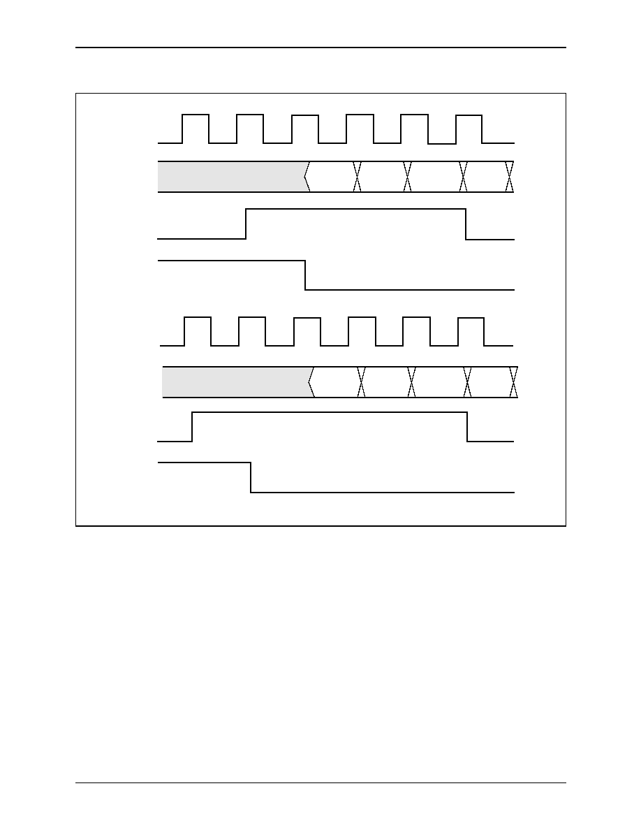
4.0 Electrical and Mechanical Specifications
CN8223
4.3 Timing
ATM Transmitter/Receiver with UTOPIA Interface
4-14
Conexant
100046C
Figure 4-7. UTOPIA Interface Timing
1
3
4
7
5
8
H1
H2
H3
H4
TxClk
TxData
TxPrty
TxSOC
TxFull
~
TxClav
TxEnb
~
2
6
RxClk
9
11
12
14
15
10
13
RxData
RxPrty
RxSOC
RxEmpty
~
RxClav
RxENB*
H1
H2
H3
H4
8223_039

CN8223
4.0 Electrical and Mechanical Specifications
ATM Transmitter/Receiver with UTOPIA Interface
4.3 Timing
100046C
Conexant
4-15
4.3.5 TAXI Interface Timing
Table 4-9
and
Figure 4-8
display the timing requirements and characteristics of
the TAXI interface. All times are in nanoseconds.
Table 4-9. TAXI Interface Timing
Name
Interval
Description
Min
Max
t
ptx
1≠5
Transmit Clock Input Period
50
--
t
tcl
1≠3
Transmit Clock High Pulse Width
25
--
t
tch
3≠5
Transmit Clock Low Pulse Width
25
--
t
clsh
3≠4
Transmit Clock Low to Strobe Output High
3.0
--
t
sh
4≠6
Strobe Output Pulse Width High
t
ptx
/2
12.0
t
cssh
2≠4
Command Out Setup before Strobe High
25
--
t
chsh
4≠7
Command Out Hold after Strobe High
24
--
t
dssh
8≠9
Data Out Setup before Strobe High
22
--
t
dhsh
9≠10
Data Out Hold after Strobe High
25
--
t
prx
11≠17
Receive Clock Input Period
50
--
t
rcl
11≠14
Receive Clock Low Pulse Width
25
--
t
rch
14≠17
Receive Clock High Pulse Width
25
--
t
ssch
12≠14
Command Strobe Setup before Clock High
4
--
t
csch
13≠14
Command Input Setup before Clock High
8
--
t
shch
14≠15
Command Strobe Hold after Clock High
0
--
t
chch
14≠16
Command Input Hold after Clock High
5
--
t
dsch
18≠19
Data/Violation Input Setup before Clock High
5
--
t
dhch
19≠20
Data/Violation Input Hold after Clock High
5
--
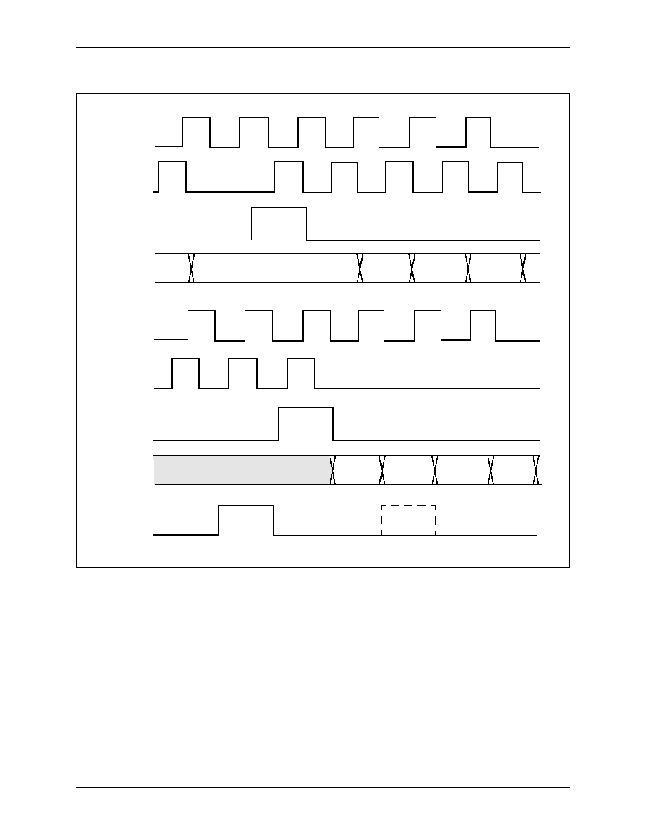
4.0 Electrical and Mechanical Specifications
CN8223
4.3 Timing
ATM Transmitter/Receiver with UTOPIA Interface
4-16
Conexant
100046C
Figure 4-8. TAXI Port Interface Timing
TXCKI
(CLK)
TXOUT[8]
(CI 1)
TXOUT[7:0]
D[7:0]
RXCKI
(CLK)
RCVHLD
(CSTRB)
RXIN[7:0]
DO [7:0]
RXIN[8]
(VLTN)
TXIN
(CO 1)
TXCLKO
(STRB)
HI
1
3
5
4
6
9
8
2
7
10
H2
H3
H4
11
14
17
19
12
15
13
16
HI
H2
H3
H4
18
20
8223_040

CN8223
4.0 Electrical and Mechanical Specifications
ATM Transmitter/Receiver with UTOPIA Interface
4.4 Mechanical Drawing
100046C
Conexant
4-17
4.4 Mechanical Drawing
The CN8223 is a 160-pin Plastic Quad Flat Pack (PQFP) as illustrated in
Figure 4-9
.
Figure 4-9. CN8223 160-Pin Plastic Quad Flat Pack
160 MQFP - 1.60/0.33 Form
TOP VIEW
BOTTOM VIEW
D
E
E1
D1
b
e
A2
A
A1
1.60
(.063)
REF.
L
S
Y
M
B
O
L
ALL DIMENSIONS
IN MILLIMETERS
A
A1
A2
D
D1
E
E1
L
e
b
MIN.
----
0.25
3.17
30.95
27.90
30.95
27.90
0.60
0.22
NOM.
----
----
3.37
31.20
28.00
31.20
28.00
----
0.65 BSC.
----
MAX.
4.20
----
3.67
31.45
28.10
31.45
28.10
1.15
0.38
8223_041

4.0 Electrical and Mechanical Specifications
CN8223
4.4 Mechanical Drawing
ATM Transmitter/Receiver with UTOPIA Interface
4-18
Conexant
100046C

10046C
Conexant
A-1
A
Appendix A: Transmit FIFO Port Rates
This appendix describes the arbitration mechanism used to control and prioritize
the Transmit FIFO port rate. The CN8223 has two options for its ATM layer
interface: UTOPIA or FIFO mode. UTOPIA mode is discussed in the body of the
data sheet. FIFO mode provides four bidirectional ports. Since they operate
independently, multiple ports may attempt to send data during the same cell slot.
When these collisions occur, the CN8223 implements an arbitration mechanism
to select which port will transmit data.
The CN8223 combines rate control and priority when selecting a port. First,
the rate control circuit determines the eligibility of the port. Then the CN8223
arbitrates between eligible ports on a priority basis. This entire process is repeated
for each cell slot. A cell which has lost arbitration due to priority may still be
determined ineligible for transmission during the next interval.
The priority and rate setting of a channel must not be changed once
transmission has begun. This will cause unpredictable behavior. It could cause a
port to stop transmitting. Users can change both priority and rate for ports during
an "idle" interval. During such an interval, all ports, including unused ports,
should assert FIFO empty flags.
A.1 Rate Control
The CN8223 provides a rate control mechanism to establish fairness. As
described in the specification, each port is assigned a maximum rate through a
register. This rate is based on a 256-cell slot interval. Each port can be allowed to
transmit on a percentage of these cell slots. This is accomplished by assigning a
rate between 0 and 255 in the TX_RATE_xx register. A rate of 0 inhibits
transmission on a port, while a rate of 255 allows transmission in any slot. This
rate establishes an upper bound on an individual port's rate. It does not guarantee
a rate for ports sharing a priority with, or at a lower priority than, other active
ports.
Table A-1
lists thresholds for each port's TX_RATE value. In a given cell slot,
these thresholds are compared with the TX_RATE_xx register for the port. If the
TX_RATE value is greater than or equal to the threshold, then the port is eligible
to transmit in that slot. Otherwise, it is ineligible. Note that each port is unique in
its transmission characteristics for a given TX_RATE value. For instance, with a
TX_RATE setting of 127 (50 %), Port 0 will be eligible for eight cells, then
ineligible for eight cells. Port 3 will be eligible every other cell. Both ports may
transmit on 50 % of the cell slots, but the burst length varies.

Appendix A: Transmit FIFO Port Rates
CN8223
A.2 Port Priority
ATM Transmitter/Receiver with UTOPIA Interface
A-2
Conexant
10046C
A.2 Port Priority
The user can define a priority for each port. This priority can range from 0 to 3,
with 0 being the highest priority. A higher priority port will always preempt one
with a lower priority. This priority is programmable for each register in bits 3≠2 of
the CELL_GEN_X register.
The user can configure multiple ports to be the same priority. Within the
lowest priority, arbitration is on a "round-robin" basis. For example, if Port 0 is
carrying CBR signals it should be assigned the highest priority. Ports 1 and 2,
carrying less jitter-sensitive data, can be programmed to a lower priority. Port 0
will preempt Ports 1 and 2 when data is available. As long as both ports have data
available, Ports 1 and 2 will alternate transmission in slots where Port 0 is not
active.
Only the lowest priority ports should share a priority. Round-robin scheduling
may break down for multiple ports sharing a priority above a lower priority port.
If the CN8223 has been transmitting at priority 1, and a priority 0 port preempts
this transmission; that priority 0 port will not share the channel with other ports. It
will continue winning arbitration until it no longer has data available. At that
time, another priority 0 or lower priority channels will be allowed to transmit.
A.3 Summary
The CN8223's transmit rate shaping is controlled via a user-assigned priority and
rate for each FIFO port. The CN8223 scheduling attempts to provide a fair
arbitration algorithm and to limit burst transmission by a single channel on the
line. A system designer should consider each data stream's characteristics when
choosing the port, priority, and rate to assign.

CN8223
Appendix A: Transmit FIFO Port Rates
ATM Transmitter/Receiver with UTOPIA Interface
A.3 Summary
10046C
Conexant
A-3
Slot
Port 0
Port 1
Port 2
Port 3
0
0
0
0
0
1
1
2
4
128
2
2
4
128
8
3
3
6
132
136
4
4
128
8
64
5
5
130
12
192
6
6
132
136
72
7
7
134
140
200
8
128
8
64
16
9
129
10
68
144
10
130
12
192
24
11
131
14
196
152
12
132
136
72
80
13
133
138
76
208
14
134
140
200
88
15
135
142
204
216
16
8
64
16
32
17
9
66
20
160
18
10
68
144
40
19
11
70
148
168
20
12
192
24
96
21
13
194
28
224
22
14
196
152
104
23
15
198
156
232
24
136
72
80
48
25
137
74
84
176
26
138
76
208
56
27
139
78
212
184
28
140
200
88
112
29
141
202
92
240
30
142
204
216
120
31
143
206
220
248
32
64
16
32
1
33
65
18
36
129
34
66
20
160
9
35
67
22
164
137
36
68
144
40
65
37
69
146
44
193
38
70
148
168
73
39
71
150
172
201
40
192
24
96
17
41
193
26
100
145
42
194
28
224
25
43
195
30
228
153
44
196
152
104
81
45
197
154
108
209
46
198
156
232
89
47
199
158
236
217
48
72
80
48
33
49
73
82
52
161
50
74
84
176
41
51
75
86
180
169
52
76
208
56
97
53
77
210
60
225
54
78
212
184
105
55
79
214
188
233
56
200
88
112
49
57
201
90
116
177
58
202
92
240
57
59
203
94
244
185
60
204
216
120
113
61
205
218
124
241
62
206
220
248
121
63
207
222
252
249
64
16
32
1
2
65
17
34
5
130
66
18
36
129
10
67
19
38
133
138
Slot
Port 0
Port 1
Port 2
Port 3
Table A-1. Cell Thresholds (1 of 4)

Appendix A: Transmit FIFO Port Rates
CN8223
A.3 Summary
ATM Transmitter/Receiver with UTOPIA Interface
A-4
Conexant
10046C
68
20
160
9
66
69
21
162
13
194
70
22
164
137
74
71
23
166
141
202
72
144
40
65
18
73
145
42
69
146
74
146
44
193
26
75
147
46
197
154
76
148
168
73
82
77
149
170
77
210
78
150
172
201
90
79
151
174
205
218
80
24
96
17
34
81
25
98
21
162
82
26
100
145
42
83
27
102
148
170
84
28
224
25
98
85
29
226
29
226
86
30
228
153
106
87
31
230
157
234
88
152
104
81
50
89
153
106
85
178
90
154
108
209
58
91
155
110
213
186
92
156
232
89
114
93
157
234
93
242
94
158
236
217
122
95
159
238
221
250
96
80
48
33
3
97
81
50
37
131
98
82
52
161
11
99
83
54
165
139
100
84
176
41
67
101
85
178
45
195
Slot
Port 0
Port 1
Port 2
Port 3
102
86
180
169
75
103
87
182
173
203
104
208
56
97
19
105
209
58
101
147
106
210
60
225
27
107
211
62
229
155
108
212
184
105
83
109
213
186
109
211
110
214
188
233
91
111
215
190
237
219
112
88
112
49
35
113
89
114
53
163
114
90
116
177
43
115
91
118
181
171
116
92
240
57
99
117
93
242
61
227
118
94
244
185
107
119
95
246
189
235
120
216
120
113
51
121
217
122
117
179
122
218
124
241
59
123
219
126
245
187
124
220
248
121
115
125
221
250
125
243
126
222
252
249
123
127
223
254
253
251
128
32
1
2
4
129
33
3
6
132
130
34
5
130
12
131
35
7
134
140
132
36
129
10
68
133
37
131
14
196
134
38
133
138
76
135
39
135
142
204
Slot
Port 0
Port 1
Port 2
Port 3
Table A-1. Cell Thresholds (2 of 4)

CN8223
Appendix A: Transmit FIFO Port Rates
ATM Transmitter/Receiver with UTOPIA Interface
A.3 Summary
10046C
Conexant
A-5
136
160
9
66
20
137
161
11
70
148
138
162
13
194
28
139
163
15
198
156
140
164
137
74
84
141
165
139
78
212
142
166
141
202
92
143
167
143
206
220
144
40
65
18
36
145
41
67
22
164
146
42
69
146
44
147
43
71
150
172
148
44
193
26
100
149
45
195
30
228
150
46
197
154
108
151
47
199
158
236
152
168
73
82
52
153
169
75
86
180
154
170
77
210
60
155
171
79
214
188
156
172
201
90
116
157
173
203
94
244
158
174
205
218
124
159
175
207
222
252
160
96
17
34
5
161
97
19
38
133
162
98
21
162
13
163
99
23
166
141
164
100
145
42
69
165
101
147
46
197
166
102
149
170
77
167
103
151
174
205
168
224
25
98
21
169
225
27
102
149
Slot
Port 0
Port 1
Port 2
Port 3
170
226
29
226
29
171
227
31
230
157
172
228
153
106
85
173
229
155
110
213
174
230
157
234
93
175
231
159
238
221
176
104
81
50
37
177
105
83
54
165
178
106
85
178
45
179
107
87
182
173
180
108
209
58
101
181
109
211
62
229
182
110
213
186
109
183
111
215
190
237
184
232
89
114
53
185
233
91
118
181
186
234
93
242
61
187
235
95
246
189
188
236
217
122
117
189
237
219
126
245
190
238
221
250
125
191
239
223
254
253
192
48
33
3
6
193
49
35
7
134
194
50
37
131
14
195
51
39
135
142
196
52
161
11
70
197
53
163
15
198
198
54
165
139
78
199
55
167
143
206
200
176
41
67
22
201
177
43
71
150
202
178
45
195
30
203
179
47
199
158
Slot
Port 0
Port 1
Port 2
Port 3
Table A-1. Cell Thresholds (3 of 4)

Appendix A: Transmit FIFO Port Rates
CN8223
A.3 Summary
ATM Transmitter/Receiver with UTOPIA Interface
A-6
Conexant
10046C
204
180
169
75
86
205
181
171
79
214
206
182
173
203
94
207
183
175
207
222
208
56
97
19
38
209
57
99
23
166
210
58
101
147
46
211
59
103
151
174
212
60
225
27
102
213
61
227
31
230
214
62
229
155
110
215
63
231
159
238
216
184
105
83
54
217
185
107
87
182
218
186
109
211
62
219
187
111
215
190
220
188
233
91
118
221
189
235
95
246
222
190
237
219
126
223
191
239
223
254
224
112
49
35
7
225
113
51
39
135
226
114
53
163
15
Slot
Port 0
Port 1
Port 2
Port 3
227
115
55
167
143
228
116
177
43
71
229
117
179
47
199
230
118
181
171
79
231
119
183
175
207
232
240
57
99
23
233
241
59
103
151
234
242
61
227
31
235
243
63
231
159
236
244
185
107
87
237
245
187
111
215
238
246
189
235
95
239
247
191
239
223
240
120
113
51
39
241
121
115
55
167
242
122
117
179
47
243
123
119
183
175
244
124
241
59
103
245
125
243
63
231
246
126
245
187
111
247
127
247
191
239
248
248
121
115
55
249
249
123
119
183
250
250
125
243
63
251
251
127
247
191
252
252
249
123
119
253
253
251
127
247
254
254
253
251
127
255
255
255
255
255
Slot
Port 0
Port 1
Port 2
Port 3
Table A-1. Cell Thresholds (4 of 4)

100046C
Conexant
B-1
B
Appendix B: Acronym List
AAL
ATM Adaptation Layer
AIS
Alarm Indication Signal
APS
Automatic Protection Switching
ATM
Asynchronous Transfer Mode
BIP-8
Octet Bit Interleaved Parity
BOM
Beginning of Message
CMOS
Complementary Metal-Oxide Semiconductor
COM
Continuation of Message
Coset
A byte with a specific value
CPE
Customer Premise Equipment
CRC
Cyclic Redundancy Check
EOM
End of Message
FAS
Frame Alignment Signal
FCS
Frame Check Sequence
FEAC
Far End Alarm Control
FEBE
Far End Block Error
FERF
Line Far End Receive Failure
FIFO
First In First Out
HDLC
High-Level Data Link Control
HEC
Header Error Control
ISR
Interrupt Service Routine
LAPD
Link Access Procedure on the D Channel
LCV
Line Code Violation
LIU
Line Interface Unit
LOC
Loss of Cell
LOCD
Loss of Cell Delineation
LOF
Loss of Frame
LOS
Loss of Signal
LSB
Least Significant Bit
MSB
Most Significant Bit
NNI
Network-to-Network Interface
NRZ
Non-Return to Zero
OOF
Out of Frame
PECL
Pseudo-Emitter Coupled Logic
PHY
Physical Interface
PLCP
Physical Layer Convergence Protocol
PMD
Physical Medium Dependent

Appendix B: Acronym List
CN8223
ATM Transmitter/Receiver with UTOPIA Interface
B-2
Conexant
100046C
POI
Path Overhead Identifier
PQFP
Plastic Quad Flat Pack
RDI
Remote Defect Indication
SDH
Synchronous Digital Hierarchy
SMDS
Switched Multimegabit Data Service
SONET
Synchronous Optical Network [an ANSI standard]
SPE
Synchronous Payload Envelope
SSM
Single Segment Message
STS
Synchronous Transport Signal
TAXI
Transparent Asynchronous Transmitter/Receiver Interface
UNI
User-to-Network Interface
UTOPIA
Universal Test And Operation Physical Interface For ATM
VCI
Virtual Channel Identifier
VPI
Virtual Path Identifier

Further Information:
literature@conexant.com
1-800-854-8099 (North America)
33-14-906-3980 (International)
Web Site
www.conexant.com
World Headquarters
Conexant Systems, Inc.
4311 Jamboree Road,
P.O. Box C
Newport Beach, CA 92658-8902
Phone: (949) 483-4600
Fax: (949) 483-6375
U.S. Florida/South America
Phone: (727) 799-8406
Fax: (727) 799-8306
U.S. Los Angeles
Phone: (805) 376-0559
Fax: (805) 376-8180
U.S. Mid-Atlantic
Phone: (215) 244-6784
Fax: (215) 244-9292
U.S. North Central
Phone: (630) 773-3454
Fax: (630) 773-3907
U.S. Northeast
Phone: (978) 692-7660
Fax: (978) 692-8185
U.S. Northwest/Pacific West
Phone: (408) 249-9696
Fax: (408) 249-7113
U.S. South Central
Phone: (972) 733-0723
Fax: (972) 407-0639
U.S. Southeast
Phone: (919) 858-9110
Fax: (919) 858-8669
U.S. Southwest
Phone: (949) 483-9119
Fax: (949) 483-9090
APAC Headquarters
Conexant Systems Singapore,
Pte. Ltd.
1 Kim Seng Promenade
Great World City
#09-01 East Tower
Singapore 237994
Phone: (65) 737 7355
Fax: (65) 737 9077
Australia
Phone: (61 2) 9869 4088
Fax: (61 2) 9869 4077
China
Phone: (86 2) 6361 2515
Fax: (86 2) 6361 2516
Hong Kong
Phone: (852) 2 827 0181
Fax: (852) 2 827 6488
India
Phone: (91 11) 692 4780
Fax: (91 11) 692 4712
Korea
Phone: (82 2) 565 2880
Fax: (82 2) 565 1440
Europe Headquarters
Conexant Systems France
Les Taissounieres B1
1681 Route des Dolines
BP 283
06905 Sophia Antipolis Cedex
France
Phone: (33 4) 93 00 33 35
Fax: (33 4) 93 00 33 03
Europe Central
Phone: (49 89) 829 1320
Fax: (49 89) 834 2734
Europe Mediterranean
Phone: (39 02) 9317 9911
Fax: (39 02) 9317 9913
Europe North
Phone: (44 1344) 486 444
Fax: (44 1344) 486 555
Europe South
Phone: (33 1) 41 44 36 50
Fax: (33 1) 41 44 36 90
Middle East Headquarters
Conexant Systems
Commercial (Israel) Ltd.
P.O. Box 12660
Herzlia 46733, Israel
Phone: (972 9) 952 4064
Fax: (972 9) 951 3924
Japan Headquarters
Conexant Systems Japan Co., Ltd.
Shimomoto Building
1-46-3 Hatsudai,
Shibuya-ku, Tokyo
151-0061 Japan
Phone: (81 3) 5371 1567
Fax: (81 3) 5371 1501
Taiwan Headquarters
Conexant Systems, Taiwan Co., Ltd.
Room 2808
International Trade Building
333 Keelung Road, Section 1
Taipei 110, Taiwan, ROC
Phone: (886 2) 2720 0282
Fax: (886 2) 2757 6760
0.0 Sales Offices