Data Sheet
100441E
October 13, 1999
CN8330
DS3/E3 Framer with 52 Mbps HDLC Controller
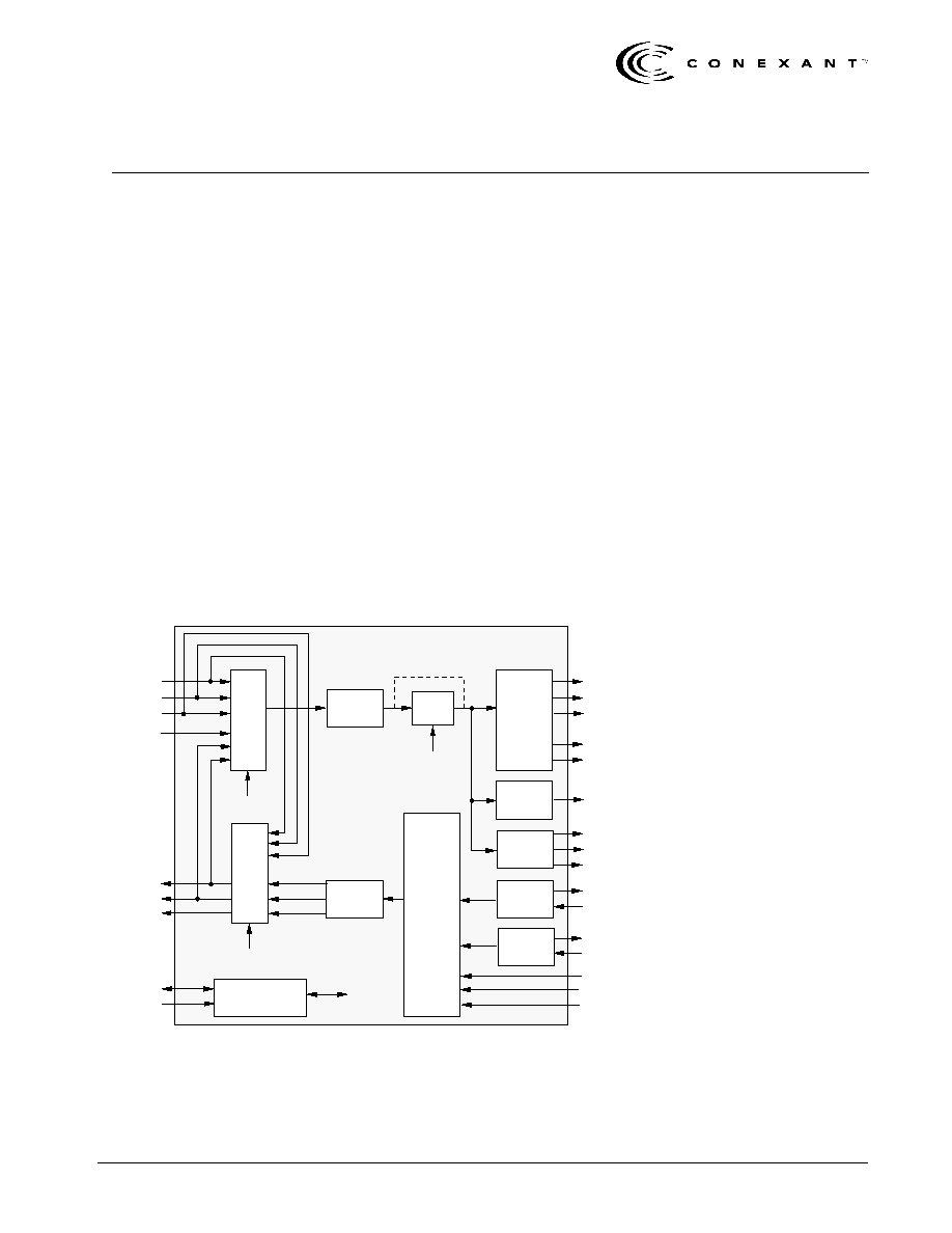
The CN8330 is an integral DS3/E3 framer designed to support the transmission
formats defined by ANSI T1.107-1988, T1.107a-1989, T1.404, and ITU-T G.751
standards. All maintenance features required by Bellcore TR-TSY-000009 and AT&T
PUB 54014 are provided. In addition, the CN8330 can be optionally configured as a
High-Level Data Link Controller (HDLC) usable with or without DS3/E3 framing
overhead.
The CN8330 provides framing recovery for M13, C-bit parity, Syntran, and G.751
E3 formatted signals. A First In First Out (FIFO) buffer in the receive path can be
enabled to reduce jitter on the incoming data. Transmit and receive data is available to
the host in either serial or parallel byte and nibble formats. Access is provided to the
terminal data link and the Far End Alarm/Control (FEAC) channel, as specified in
T1.107a-1989. Counters are included for frame-bit errors, Line Code Violations
(LCVs), parity errors, and Far End Block Errors (FEBEs).
Two operational modes are available: microprocessor and stand-alone monitor
control modes. The microprocessor control mode monitors all status conditions and
provides configuration control. The stand-alone monitor mode allows the CN8330 to
operate as a monitor providing status and alarm information on external pins.
Functional Block Diagram
M
U
X
Source
Loopback
Unipolar
Conversion
FIFO
FIFO
Enable
RXMSY
CBITO
RXCCK
RXDAT
RXCLK
Framing
Recovery
Overhead/
Data Link
Processing
Status
PPDL
Receiver
RDAT[7:0]
RXBCK
Status
PPDL
Transmitter
Bipolar
Encoder
Framing/
Overhead
Insertion
Overhead/
Data Link
Processing
Line
Loopback
TXPOS
TXNEG
TCLKO
Microprocessor
Interface
AD[7:0]
Control
TXBCK
TDAT[7:0]
TXCCK
CBITI
TXCKI
TXDATI
TXSYI
To/From
All Blocks
Bypass
M
U
X
RXPOS
RXNEG
DS3CKI
TXCKI
Distinguishing Features
∑
Supports DS3/E3 framing modes
∑
Includes high-speed HDLC controller
(52 MHz)
∑
Framing recovery for M13, C-bit
parity, Syntran, and G.751 E3 signals
∑
Serial or parallel (octet or nibble)
interface modes
∑
Average reframe time of less than
1 ms for DS3 and less than 250 µs
for E3
∑
Supports the LAPD terminal data link
and FEAC channel as defined in
T1.107a-1989
∑
68-pin PLCC or 80-pin MQFP
surface-mount package
∑
Operates from a single +5 VDC ±5%
power supply
∑
Low-power CMOS technology
Applications
∑
Digital PCM switches
∑
Digital Cross-Connect Systems
∑
Channel Service Units (CSUs)
∑
Channel extenders
∑
ATM Switches/Concentrators
∑
PBXs
∑
Switched Multimegabit Digital
Service (SMDS) Equipment
∑
Test equipment
∑
Routers (including HSSI ports)
100441E
Conexant
Information provided by Conexant Systems, Inc. (Conexant) is believed to be accurate and reliable. However, no responsibility is
assumed by Conexant for its use, nor any infringement of patents or other rights of third parties which may result from its use. No
license is granted by implication or otherwise under any patent rights of Conexant other than for circuitry embodied in Conexant
products. Conexant reserves the right to change circuitry at any time without notice. This document is subject to change without
notice.
Conexant products are not designed or intended for use in life support appliances, devices, or systems where malfunction of a
Conexant product can reasonably be expected to result in personal injury or death. Conexant customers using or selling Conexant
products for use in such applications do so at their own risk and agree to fully indemnify Conexant for any damages resulting from
such improper use or sale.
The trademarks "Conexant" and the Conexant symbol are trademarks of Conexant Systems, Inc.
Product names or services listed in this publication are for identification purposes only, and may be trademarks or registered
trademarks of their respective companies. All other marks mentioned herein are the property of their respective holders.
© 1999 Conexant Systems, Inc.
Printed in U.S.A.
All Rights Reserved
Reader Response: Conexant strives to produce quality documentation, and welcomes your feedback. Please send
comments and suggestions to
conexant.tech.pubs@conexant.com
. For technical questions, contact your local
Conexant
sales office
or field applications engineer.
Ordering Information
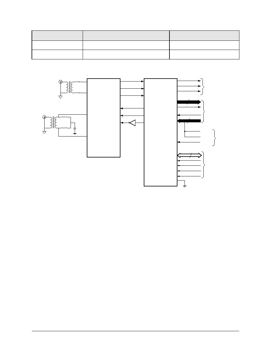
CN8330 Typical DS3 Application
Model Number
Package
Ambient Temperature
CN8330EPJD
68-Pin Plastic Leaded Chip Carrier (PLCC)
≠40 to 85
∞
C
CN8330EPD
80-Pin Metric Quad Flat Pack (MQFP)
≠40 to 85
∞
C
CN8331
CN8330
DS3/E3 Framer
TPOS1
TNEG1
TCLK1
RLINE1P
RLINE1N
TLINE1P
TLINE1N
RXDAT
RXCLK
RXMSY
RXPOS
RXNEG
DS3CKI
TXPOS
TXNEG
TCLKO
Receive
Serial
Data
Interface
31.6
31.6
0.01
37.4
37.4
RPOS1
RNEG1
RCLK1
RDAT[7:0]
RXBCK
TXBCK
TDAT[7:0]
8
Parallel
Data
Interface
(Also used
for HDLC
payload
data)
TDAT7
TDAT6
8
(M-Sync)
(Data)
(Clock)
Transmit
Serial
Data
Interface
8
AD[7:0]
RD*
WR*
CS
ALE
Microprocessor
Interface
TXCKI
MON/MIC*

100441E
Conexant
i
Table of Contents
List of Figures
. . . . . . . . . . . . . . . . . . . . . . . . . . . . . . . . . . . . . . . . . . . . . . . . . . . . . . . . . . . . . . . . . . . . . . . . . v
List of Tables
. . . . . . . . . . . . . . . . . . . . . . . . . . . . . . . . . . . . . . . . . . . . . . . . . . . . . . . . . . . . . . . . . . . . . . . . . vii
1.0
Product Description
. . . . . . . . . . . . . . . . . . . . . . . . . . . . . . . . . . . . . . . . . . . . . . . . . . . . . . . . . . . . . 1-1
1.1
Pin Descriptions
. . . . . . . . . . . . . . . . . . . . . . . . . . . . . . . . . . . . . . . . . . . . . . . . . . . . . . . . . . . . 1-3
2.0
Functional Description
. . . . . . . . . . . . . . . . . . . . . . . . . . . . . . . . . . . . . . . . . . . . . . . . . . . . . . . . . . 2-1
2.1
Overview
. . . . . . . . . . . . . . . . . . . . . . . . . . . . . . . . . . . . . . . . . . . . . . . . . . . . . . . . . . . . . . . . . . 2-1
2.1.1
Brief Block Description
. . . . . . . . . . . . . . . . . . . . . . . . . . . . . . . . . . . . . . . . . . . . . . . . . . 2-1
2.1.2
Clock Interface and Initialization
. . . . . . . . . . . . . . . . . . . . . . . . . . . . . . . . . . . . . . . . . . . 2-3
2.1.2.1
Initialization
. . . . . . . . . . . . . . . . . . . . . . . . . . . . . . . . . . . . . . . . . . . . . . . . . 2-3
2.1.3
Microprocessor Interface
. . . . . . . . . . . . . . . . . . . . . . . . . . . . . . . . . . . . . . . . . . . . . . . . 2-3
2.1.3.1
Using with Specific Microcontrollers
. . . . . . . . . . . . . . . . . . . . . . . . . . . . . . . 2-3
2.1.3.2
Microprocessor Interrupts
. . . . . . . . . . . . . . . . . . . . . . . . . . . . . . . . . . . . . . . 2-4
2.1.3.3
Address Map
. . . . . . . . . . . . . . . . . . . . . . . . . . . . . . . . . . . . . . . . . . . . . . . . 2-4
2.2
Line Interfaces
. . . . . . . . . . . . . . . . . . . . . . . . . . . . . . . . . . . . . . . . . . . . . . . . . . . . . . . . . . . . . 2-5
2.2.1
Transmitter Line Interface
. . . . . . . . . . . . . . . . . . . . . . . . . . . . . . . . . . . . . . . . . . . . . . . . 2-5
2.2.2
Receiver Line Interface
. . . . . . . . . . . . . . . . . . . . . . . . . . . . . . . . . . . . . . . . . . . . . . . . . . 2-6
2.3
Transmitter Operation
. . . . . . . . . . . . . . . . . . . . . . . . . . . . . . . . . . . . . . . . . . . . . . . . . . . . . . . . 2-7
2.3.1
Input and Synchronization
. . . . . . . . . . . . . . . . . . . . . . . . . . . . . . . . . . . . . . . . . . . . . . . 2-7
2.3.2
DS3 Mode
. . . . . . . . . . . . . . . . . . . . . . . . . . . . . . . . . . . . . . . . . . . . . . . . . . . . . . . . . . . 2-7
2.3.3
E3 Mode
. . . . . . . . . . . . . . . . . . . . . . . . . . . . . . . . . . . . . . . . . . . . . . . . . . . . . . . . . . . . 2-9
2.3.4
Framing Bit Generation
. . . . . . . . . . . . . . . . . . . . . . . . . . . . . . . . . . . . . . . . . . . . . . . . . 2-10
2.3.5
Alarm Signal Generation
. . . . . . . . . . . . . . . . . . . . . . . . . . . . . . . . . . . . . . . . . . . . . . . . 2-11
2.3.6
Terminal Data Link Transmitter
. . . . . . . . . . . . . . . . . . . . . . . . . . . . . . . . . . . . . . . . . . . 2-12
2.3.6.1
Sending a Message
. . . . . . . . . . . . . . . . . . . . . . . . . . . . . . . . . . . . . . . . . . . 2-13
2.3.6.2
Aborting a Message
. . . . . . . . . . . . . . . . . . . . . . . . . . . . . . . . . . . . . . . . . . 2-14
2.3.6.3
Transmitter Interrupts
. . . . . . . . . . . . . . . . . . . . . . . . . . . . . . . . . . . . . . . . . 2-14
2.3.6.4
Transmitter Control Example
. . . . . . . . . . . . . . . . . . . . . . . . . . . . . . . . . . . . 2-15
2.3.7
TxFEAC Channel Transmission
. . . . . . . . . . . . . . . . . . . . . . . . . . . . . . . . . . . . . . . . . . . 2-15
2.3.8
PPDL Transmitter
. . . . . . . . . . . . . . . . . . . . . . . . . . . . . . . . . . . . . . . . . . . . . . . . . . . . . 2-16
2.3.9
PPDLONLY Mode
. . . . . . . . . . . . . . . . . . . . . . . . . . . . . . . . . . . . . . . . . . . . . . . . . . . . . 2-20
2.3.10
Transmitter Outputs
. . . . . . . . . . . . . . . . . . . . . . . . . . . . . . . . . . . . . . . . . . . . . . . . . . . 2-20
2.3.11
Test Equipment Specific Features
. . . . . . . . . . . . . . . . . . . . . . . . . . . . . . . . . . . . . . . . . 2-21

CN8330
DS3/E3 Framer with 52 Mbps HDLC Controller
ii
Conexant
100441E
2.4
Receiver Operation
. . . . . . . . . . . . . . . . . . . . . . . . . . . . . . . . . . . . . . . . . . . . . . . . . . . . . . . . . 2-22
2.4.1
Bipolar-to-Unipolar Conversion
. . . . . . . . . . . . . . . . . . . . . . . . . . . . . . . . . . . . . . . . . . . 2-22
2.4.2
Receive FIFO
. . . . . . . . . . . . . . . . . . . . . . . . . . . . . . . . . . . . . . . . . . . . . . . . . . . . . . . . 2-22
2.4.3
Received Signal Output
. . . . . . . . . . . . . . . . . . . . . . . . . . . . . . . . . . . . . . . . . . . . . . . . 2-23
2.4.4
Framing Operation
. . . . . . . . . . . . . . . . . . . . . . . . . . . . . . . . . . . . . . . . . . . . . . . . . . . . 2-25
2.4.5
Alarm Detection
. . . . . . . . . . . . . . . . . . . . . . . . . . . . . . . . . . . . . . . . . . . . . . . . . . . . . . 2-25
2.4.6
Terminal Data Link Reception
. . . . . . . . . . . . . . . . . . . . . . . . . . . . . . . . . . . . . . . . . . . . 2-26
2.4.6.1
Receiver Interrupts
. . . . . . . . . . . . . . . . . . . . . . . . . . . . . . . . . . . . . . . . . . . 2-28
2.4.6.2
Receiver Response Example
. . . . . . . . . . . . . . . . . . . . . . . . . . . . . . . . . . . . 2-28
2.4.7
RxFEAC Channel Reception
. . . . . . . . . . . . . . . . . . . . . . . . . . . . . . . . . . . . . . . . . . . . . . 2-29
2.4.8
PPDL Receiver
. . . . . . . . . . . . . . . . . . . . . . . . . . . . . . . . . . . . . . . . . . . . . . . . . . . . . . . 2-30
2.4.9
PPDLONLY Mode
. . . . . . . . . . . . . . . . . . . . . . . . . . . . . . . . . . . . . . . . . . . . . . . . . . . . . 2-32
2.4.10
Serial C-Bit Output
. . . . . . . . . . . . . . . . . . . . . . . . . . . . . . . . . . . . . . . . . . . . . . . . . . . . 2-33
2.5
Monitor Mode for Stand-Alone Operation
. . . . . . . . . . . . . . . . . . . . . . . . . . . . . . . . . . . . . . . . 2-34
2.5.1
DS3 Monitor Mode Error Outputs
. . . . . . . . . . . . . . . . . . . . . . . . . . . . . . . . . . . . . . . . . 2-35
3.0
Registers
. . . . . . . . . . . . . . . . . . . . . . . . . . . . . . . . . . . . . . . . . . . . . . . . . . . . . . . . . . . . . . . . . . . . . . 3-1
3.1
Control Registers
. . . . . . . . . . . . . . . . . . . . . . . . . . . . . . . . . . . . . . . . . . . . . . . . . . . . . . . . . . . 3-1
0x00--Mode Control Register (CR00)
. . . . . . . . . . . . . . . . . . . . . . . . . . . . . . . . . . . . . . . 3-1
0x01--Terminal Data Link Control Register (CR01)
. . . . . . . . . . . . . . . . . . . . . . . . . . . . . 3-3
0x02--Status Interrupt Control Register (CR02)
. . . . . . . . . . . . . . . . . . . . . . . . . . . . . . . 3-3
0x03--Transmit FEAC Channel Byte (CR03)
. . . . . . . . . . . . . . . . . . . . . . . . . . . . . . . . . . 3-4
0x04--Feature Control Register (CR04)
. . . . . . . . . . . . . . . . . . . . . . . . . . . . . . . . . . . . . 3-4
0x05--PPDL Control Register (CR05)
. . . . . . . . . . . . . . . . . . . . . . . . . . . . . . . . . . . . . . . 3-5
3.2
Status Registers
. . . . . . . . . . . . . . . . . . . . . . . . . . . . . . . . . . . . . . . . . . . . . . . . . . . . . . . . . . . . 3-6
0x10--DS3/E3 Maintenance Status Register (SR00)
. . . . . . . . . . . . . . . . . . . . . . . . . . . . 3-6
0x11--Counter Interrupt Status Register (SR01)
. . . . . . . . . . . . . . . . . . . . . . . . . . . . . . . 3-7
0x12--Data Link Interrupt Status Register (SR02)
. . . . . . . . . . . . . . . . . . . . . . . . . . . . . 3-8
0x13--Receive FEAC Channel Byte (SR03)
. . . . . . . . . . . . . . . . . . . . . . . . . . . . . . . . . . . 3-8
0x14--Terminal Data Link Status Register (SR04)
. . . . . . . . . . . . . . . . . . . . . . . . . . . . . . 3-9
0x15--Part Number/Hardware Version Register (SR05)
. . . . . . . . . . . . . . . . . . . . . . . . . 3-9
0x16--Shadow Status Register (SR06)
. . . . . . . . . . . . . . . . . . . . . . . . . . . . . . . . . . . . 3-10
0x20≠0x26--DS3/E3 Error Counters
. . . . . . . . . . . . . . . . . . . . . . . . . . . . . . . . . . . . . . . 3-11
0x20--DS3 Parity Error Counter (SR07)
. . . . . . . . . . . . . . . . . . . . . . . . . . . . . . . . . . . . 3-11
0x21--DS3 Disagreement Counter (SR08)
. . . . . . . . . . . . . . . . . . . . . . . . . . . . . . . . . . 3-12
0x22--DS3/E3 Frame Error Counter (SR09)
. . . . . . . . . . . . . . . . . . . . . . . . . . . . . . . . . 3-12
0x23--DS3 Path Parity Error Counter (SR10)
. . . . . . . . . . . . . . . . . . . . . . . . . . . . . . . . 3-12
0x24--DS3 FEBE Event Counter (SR11)
. . . . . . . . . . . . . . . . . . . . . . . . . . . . . . . . . . . . 3-13
0x25,0x26--DS3/E3 LCV Counter--Low and High Bytes (SR12,SR13)
. . . . . . . . . . . . . 3-13
3.3
Memory Registers
. . . . . . . . . . . . . . . . . . . . . . . . . . . . . . . . . . . . . . . . . . . . . . . . . . . . . . . . . 3-14
0x30≠0x37--Transmit Terminal Data Link Message Buffer (TxTDL)
. . . . . . . . . . . . . . . . 3-14
0x40≠0x47--Receive Terminal Data Link Message Buffer (RxTDL)
. . . . . . . . . . . . . . . . 3-14
3.4
Register Summary
. . . . . . . . . . . . . . . . . . . . . . . . . . . . . . . . . . . . . . . . . . . . . . . . . . . . . . . . . 3-15

CN8330
DS3/E3 Framer with 52 Mbps HDLC Controller
100441E
Conexant
iii
4.0
Mechanical/Electrical Specifications
. . . . . . . . . . . . . . . . . . . . . . . . . . . . . . . . . . . . . . . . . . . . . 4-1
4.1
Timing Requirements
. . . . . . . . . . . . . . . . . . . . . . . . . . . . . . . . . . . . . . . . . . . . . . . . . . . . . . . . 4-1
4.2
Environmental Conditions
. . . . . . . . . . . . . . . . . . . . . . . . . . . . . . . . . . . . . . . . . . . . . . . . . . . . . 4-5
4.2.1
Power Requirements and Temperature Range
. . . . . . . . . . . . . . . . . . . . . . . . . . . . . . . . . 4-5
4.3
Electrical Characteristics
. . . . . . . . . . . . . . . . . . . . . . . . . . . . . . . . . . . . . . . . . . . . . . . . . . . . . 4-6
4.3.1
DC Characteristics
. . . . . . . . . . . . . . . . . . . . . . . . . . . . . . . . . . . . . . . . . . . . . . . . . . . . . 4-6
4.4
Mechanical Specifications
. . . . . . . . . . . . . . . . . . . . . . . . . . . . . . . . . . . . . . . . . . . . . . . . . . . . 4-8
Appendix A Multimegabit HDLC Formatter
. . . . . . . . . . . . . . . . . . . . . . . . . . . . . . . . . . . . . . . . . . . . . . A-1
A.1
Introduction
. . . . . . . . . . . . . . . . . . . . . . . . . . . . . . . . . . . . . . . . . . . . . . . . . . . . . . . . . . . . . . . A-1
A.2
Block and Logic Diagrams
. . . . . . . . . . . . . . . . . . . . . . . . . . . . . . . . . . . . . . . . . . . . . . . . . . . . . A-3
A.3
PPDL Transmitter
. . . . . . . . . . . . . . . . . . . . . . . . . . . . . . . . . . . . . . . . . . . . . . . . . . . . . . . . . . . A-6
A.3.1
PPDL Receiver
. . . . . . . . . . . . . . . . . . . . . . . . . . . . . . . . . . . . . . . . . . . . . . . . . . . . . . . A-7
Appendix B
. . . . . . . . . . . . . . . . . . . . . . . . . . . . . . . . . . . . . . . . . . . . . . . . . . . . . . . . . . . . . . . . . . . . . . . . . . B-1
B.1
DS3CKI Clock Duty Cycle
. . . . . . . . . . . . . . . . . . . . . . . . . . . . . . . . . . . . . . . . . . . . . . . . . . . . . . B-1
B.2
Overhead Bit Insertion in E3 Parallel Payload Mode
. . . . . . . . . . . . . . . . . . . . . . . . . . . . . . . . . B-1
B.3
HDLC Formatter Mode Support While Configured for E3 Framing
. . . . . . . . . . . . . . . . . . . . . . . B-2
Appendix C
. . . . . . . . . . . . . . . . . . . . . . . . . . . . . . . . . . . . . . . . . . . . . . . . . . . . . . . . . . . . . . . . . . . . . . . . . . C-1