Data Sheet
Advance Information
N8380DSA
April 26, 1999
Advance Information
This document contains information on a product under development. The parametric information
contains target parameters that are subject to change.
CN8380
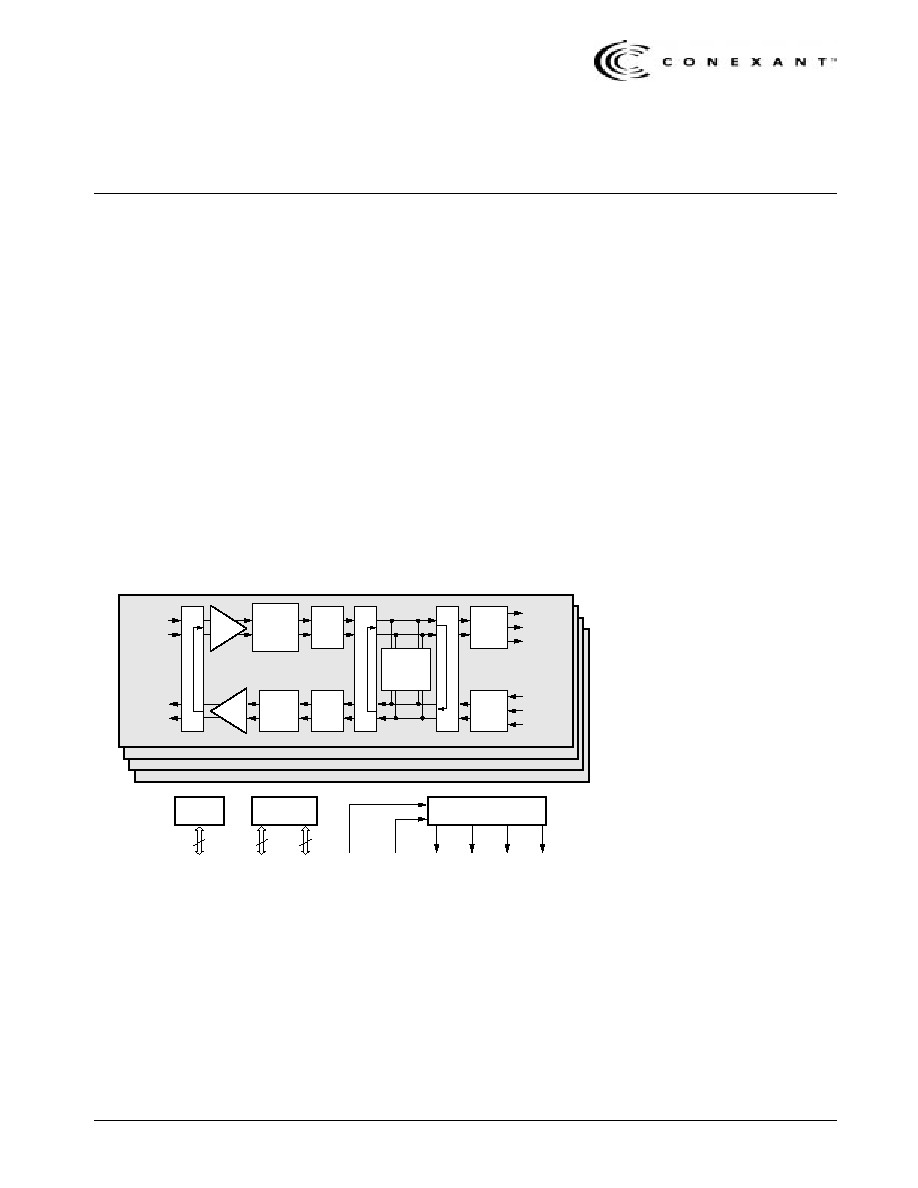
Quad T1/E1 Line Interface
The CN8380 is a fully integrated quad line interface unit for both 1.544 Mbps (T1) and
2.048 Mbps (E1) applications. It is designed to complement T1/E1 framers or operate as
a stand-alone line interface to synchronous or plesiochronous mappers and
multiplexers. The device can be controlled through a host mode serial port or by
hardware mode operation, where device control and status are obtained through
non-multiplexed dedicated pins. Many of these pins are also dedicated to individual
channels for maximum flexibility and for use in redundant systems. Integrated in the
CN8380 device is a clock rate adapter (CLAD), which provides various low-jitter
programmable system clock outputs. The receive section of the CN8380 is designed to
recover encoded signals from lines having up to 12 dB of attenuation. The transmit
section consists of a programmable, precision pulse shaper.
Functional Block Diagram
RPOSO[1]
RCKO[1]
TCLK[1]
TPOSI[1]
TNEGI[1]
RNEGO[1]
XTIP[1]
XRING[1]
RTIP[1]
RRING[1]
LIU #1
LIU #2
LIU #3
LIU #4
Clock Rate Adapter
Control
JTAG
Test Port
5
47
4
Pulse
Shaping
Driver
Jitter
Attenuator
ZCS
Decode
Local Analog Loopback
Re-
ceiver
TAIS
Clock
and
Data
Recovery
RLOS
Detect
Remote Line Loopback
Local Digital Loopback
ZCS
Decode
JTAG
Test
Signals
Control and
Alarm Signals
Host
Serial
Port
10 MHz
Fixed
Reference
Variable
Reference
1.544
MHz
2.048
MHz
32.768
MHz
8 kHz≠32 MHz
Selectable
8380_001
Distinguishing Features
∑
Four T1/E1 short haul line interfaces
in a single chip
∑
On-chip CLAD /system synchronizer
∑
Digital (crystal-less) jitter attenuators
selectable for transmitter/receiver on
each line interface
∑
Meets AT&T pub 62411 jitter specs
∑
Meets ITU G.703, ETS 300 011
(PSTNX) Connections
∑
AMI/B8ZS/HDB3 line codes
∑
Host serial port or hardware only
control modes
∑
On-chip receive clock recovery
∑
Common transformers for 120/75
E1 and 100
T1
∑
Low-power 3.3 V power supply
∑
Transmitter performance monitor
∑
Compatible with latest ANSI, ITU-T,
and ETSI standards
∑
128-pin MQFP package
∑
Remote and local loopbacks
Applications
∑
SONET/SDH multiplexers
∑
T3 and E3/E4 (PDH) multiplexers
∑
ATM multiplexers
∑
Voice compression and voice
processing equipment
∑
WAN routers and bridges
∑
Digital loop carrier terminals (DLC)
∑
HDSL terminal units
∑
Remote concentrators
∑
Central office equipment
∑
PBXs and rural switches
∑
PCM/voice channel banks
∑
Digital access and cross-connect
systems (DACS)

N8380DSA
Conexant
Advance Information
Information provided by Conexant Systems, Inc. (Conexant) is believed to be accurate and reliable. However, no responsibility is
assumed by Conexant for its use, nor any infringement of patents or other rights of third parties which may result from its use. No
license is granted by implication or otherwise under any patent rights of Conexant other than for circuitry embodied in Conexant
products. Conexant reserves the right to change circuitry at any time without notice. This document is subject to change without
notice.
Conexant and "What's Next in Communications Technologies" are trademarks of Conexant Systems, Inc.
Product names or services listed in this publication are for identification purposes only, and may be trademarks or registered
trademarks of their respective companies. All other marks mentioned herein are the property of their respective holders.
© 1999 Conexant Systems, Inc.
Printed in U.S.A.
All Rights Reserved
Reader Response: To improve the quality of our publications, we welcome your feedback. Please send comments or
suggestions via e-mail to
Conexant Reader Response@conexant.com
. Sorry, we can't answer your technical
questions at this address. Please contact your local Conexant
sales office
or local field applications engineer if you
have technical questions.
Ordering Information
Revision History
Model Number
Package
Operating Temperature
CN8380EPF
128-pin MQFP
≠40 ∞C to +85 ∞C
CN8398EVM
BT00≠D660≠001
Revision
Level
Date
Description
A
Advance
April 26, 1999
Created
N8380DSA
Conexant
Advance Information
Detailed Feature Summary
Interface Compatibility
∑
T1.102≠1993
∑
G.703 at 1.544 or 2.048 Mbps
∑
ITU-T Recommendation I.431
Receive Line Interface
∑
External Termination
∑
Equalizer compensation for ≠ 20 dB
bridged monitor levels
∑
+ 3 dB to ≠12 dB receiver sensitivity
Transmit Line Interface
∑
Pulse shapes for 0≠655 ft., in 133 ft.
steps (T1 DSX≠1)
∑
External termination for improved
return loss
∑
Line driver enable/disable for
protection switching
∑
Output short circuit protection (for
BABT applications)
Jitter Attenuator Elastic Store
∑
Receive or transmit direction
∑
8-, 16-, 32-, 64-, or 128-bit depth
∑
Automatic and manual centering
Line Codes
∑
Bipolar alternate mark inversion line
coding
∑
Optional zero code suppression:
≠ Independent transmit and receive
≠ T1: B8ZS
≠ E1: HDB3
Loopbacks
∑
Remote loopback towards line
≠ With or without JAT
≠ Retains BPV transparency
∑
Local loopback towards system
≠ Analog line loopback
≠ Local digital loopback
∑
Simultaneous local and remote line
loopbacks
Clock Rate Adapter
∑
Outputs jitter attenuated line rate
clock
≠ CLK1544 = 1544 k (T1)
≠ CLK2048 = 2048 k (E1)
∑
CLAD output supports 14 output
clock frequencies: 8 kHz to
32,768 kHz
∑
Programmable input timing
reference:
≠ Receive recovered clock from any
channel
≠ Internal clock (REFCKI)
≠ CLADI
∑
Subrate CLADI timing reference:
≠ Line rate
˜
2
N
, N = 0 to 7
≠ References as low as 8 kHz
Host Serial Interface
∑
Compatible with existing framers
∑
Compatible with microprocessor
serial ports
∑
Bit rates up to 8 Mbps
In-Service Performance Monitoring
∑
Transmit alarm detectors:
≠ Loss of Transmit Clock (TLOC)
≠ Transmit Short Circuit (TSHORT)
∑
Receive alarm detectors:
≠ Loss of Signal (RLOS)
≠ Loss of Analog Input (RALOS)
≠ Bipolar/Line Code Violations
∑
Automatic and on-demand transmit
alarms:
≠ AIS following TLOC
≠ Automatic AIS clock switching
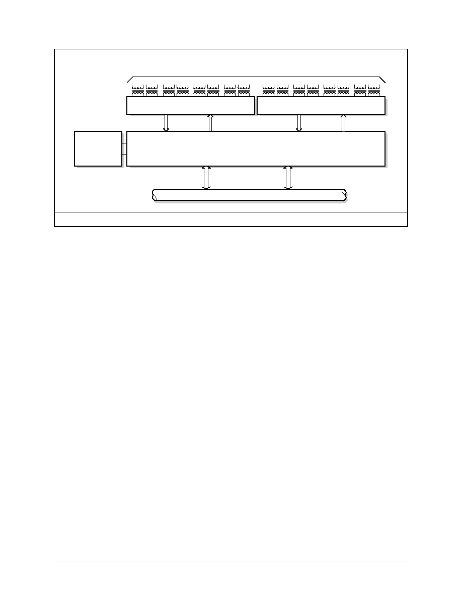
CN8398EVM Octal T1/E1 Evaluation Module
Contact a Conexant representative for EVM availability and price.
CN8380 Quad T1/E1 LIU
CN8380 Quad T1/E1 LIU
CN8398 Octal T1/E1 Framer
Local PCM Highway (i.e., 2 @ 8192 kbps)
Microprocessor
Control
Eight RJ48C T1 or E1 Line Connections
8380_002

N8380DSA
Conexant
v
Advance Information
Table of Contents
List of Figures
. . . . . . . . . . . . . . . . . . . . . . . . . . . . . . . . . . . . . . . . . . . . . . . . . . . . . . . . . . . . . . . . . . . . . . . . . ix
List of Tables
. . . . . . . . . . . . . . . . . . . . . . . . . . . . . . . . . . . . . . . . . . . . . . . . . . . . . . . . . . . . . . . . . . . . . . . . . . x i
1.0 Pin Descriptions
. . . . . . . . . . . . . . . . . . . . . . . . . . . . . . . . . . . . . . . . . . . . . . . . . . . . . . . . . . . . . . . . 1-1
2.0 Circuit Description
. . . . . . . . . . . . . . . . . . . . . . . . . . . . . . . . . . . . . . . . . . . . . . . . . . . . . . . . . . . . . . 2-1
2.1 Overview
. . . . . . . . . . . . . . . . . . . . . . . . . . . . . . . . . . . . . . . . . . . . . . . . . . . . . . . . . . . . . . . . . . 2-1
2.2 Configuration and Control
. . . . . . . . . . . . . . . . . . . . . . . . . . . . . . . . . . . . . . . . . . . . . . . . . . . . . 2-3
2.2.1 Hardware Mode
. . . . . . . . . . . . . . . . . . . . . . . . . . . . . . . . . . . . . . . . . . . . . . . . . . . . . . . 2-3
2.2.2 Host Mode
. . . . . . . . . . . . . . . . . . . . . . . . . . . . . . . . . . . . . . . . . . . . . . . . . . . . . . . . . . . 2-3
2.2.3 Host Serial Control Interface
. . . . . . . . . . . . . . . . . . . . . . . . . . . . . . . . . . . . . . . . . . . . . . 2-3
2.2.4 Reset
. . . . . . . . . . . . . . . . . . . . . . . . . . . . . . . . . . . . . . . . . . . . . . . . . . . . . . . . . . . . . . . 2-4
2.2.4.1 Power-on Reset
. . . . . . . . . . . . . . . . . . . . . . . . . . . . . . . . . . . . . . . . . . . . . . 2-5
2.2.4.2 Hard Reset
. . . . . . . . . . . . . . . . . . . . . . . . . . . . . . . . . . . . . . . . . . . . . . . . . . 2-5
2.2.4.3 Soft Reset
. . . . . . . . . . . . . . . . . . . . . . . . . . . . . . . . . . . . . . . . . . . . . . . . . . . 2-5
2.3 Receiver
. . . . . . . . . . . . . . . . . . . . . . . . . . . . . . . . . . . . . . . . . . . . . . . . . . . . . . . . . . . . . . . . . . 2-6
2.3.1 Data Recovery
. . . . . . . . . . . . . . . . . . . . . . . . . . . . . . . . . . . . . . . . . . . . . . . . . . . . . . . . 2-6
2.3.1.1 Raw Receive Mode
. . . . . . . . . . . . . . . . . . . . . . . . . . . . . . . . . . . . . . . . . . . . 2-7
2.3.1.2 Sensitivity
. . . . . . . . . . . . . . . . . . . . . . . . . . . . . . . . . . . . . . . . . . . . . . . . . . . 2-7
2.3.1.3 Bridge Mode
. . . . . . . . . . . . . . . . . . . . . . . . . . . . . . . . . . . . . . . . . . . . . . . . . 2-7
2.3.1.4 Loss Of Signal Detector
. . . . . . . . . . . . . . . . . . . . . . . . . . . . . . . . . . . . . . . . . 2-8
2.3.2 Clock Recovery
. . . . . . . . . . . . . . . . . . . . . . . . . . . . . . . . . . . . . . . . . . . . . . . . . . . . . . . 2-8
2.3.2.1 Phase Lock Loop
. . . . . . . . . . . . . . . . . . . . . . . . . . . . . . . . . . . . . . . . . . . . . 2-8
2.3.2.2 Jitter Tolerance
. . . . . . . . . . . . . . . . . . . . . . . . . . . . . . . . . . . . . . . . . . . . . . . 2-8
2.3.3 Receive Jitter Attenuator
. . . . . . . . . . . . . . . . . . . . . . . . . . . . . . . . . . . . . . . . . . . . . . . . . 2-8
2.3.4 RZCS Decoder
. . . . . . . . . . . . . . . . . . . . . . . . . . . . . . . . . . . . . . . . . . . . . . . . . . . . . . . . 2-9
2.3.5 Receive Digital Interface
. . . . . . . . . . . . . . . . . . . . . . . . . . . . . . . . . . . . . . . . . . . . . . . . . 2-9
2.3.5.1 Bipolar Mode
. . . . . . . . . . . . . . . . . . . . . . . . . . . . . . . . . . . . . . . . . . . . . . . . 2-9
2.3.5.2 Unipolar Mode
. . . . . . . . . . . . . . . . . . . . . . . . . . . . . . . . . . . . . . . . . . . . . . . 2-9
