TM
Virtual Components for the Converging World
Amphion continues to expand its family of application-specific cores
1
See http://www.amphion.com for a current list of products
CS3110/12
Reed-Solomon Encoders
The CS3110 and CS3112 Reed-Solomon encoders are designed to provide high performance solutions for a broad
range of applications requiring forward error correction. These application specific cores are developed for high
data rate digital video and audio, satellite broadcast or data storage and retrieval applications and are fully
compliant with the European DVB (CS3110) and IntelSat (CS3112) Standards. The cores are configurable Reed-
Solomon encoders featuring user-selectable codeword length (50-255 symbols) and number of parity symbols
(0-20 symbols) providing up to 1.6 Gigabits per second data throughput. The CS3110 and CS3112 are available in
both ASIC and programmable logic versions that have been handcrafted by Amphion for optimal performance
while minimizing power consumption and silicon area.
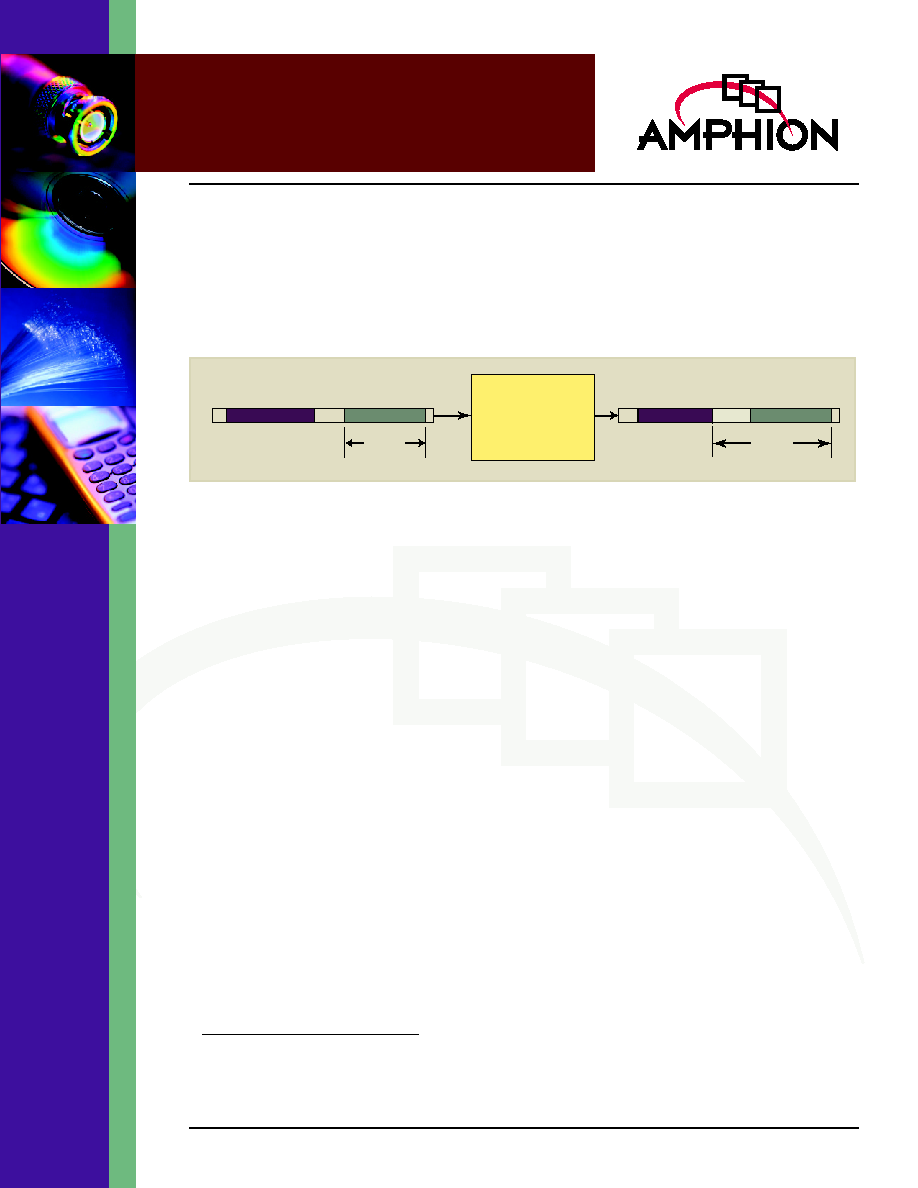
Figure 1: CS3110/12 Function
Input Data Steam
symbols
K=30-255
K
2
K
1
Output Data Stream
symbols
N=50-255
CS3110
or
CS3112
K
2
K
1
Parity
ENCODER FEATURES
Configurable Codeword Length (N) and
Number of Parity Symbols (T)
-
N = 50 � 255 symbols
-
T = 0 � 20 symbols
-
Single implementation supports any valid
block length and parity length
High Performance Solution for High Data Rate
Reed Solomon Encoding
-
Can process burst and continuous data
-
Low latency � 2 clock cycles
Supports a Range of Standards, Including
Intelsat IESS 308/309, European DVB
Telecommunication Standards ETS 300-421
and ETS 300-429
Byte-Wide Input and Output, Clocked by a
Single Symbol Rate Clock
Ease of Integration
-
Tapeout-ReadyTM firm-IP targeted netlist
-
Simple core interface for easy integration into
larger systems
KEY METRICS AND
SPECIFICATIONS
Size:
15.5k Gates
Maximum Frequency:
200 MHz
1
8 Bits per Symbol Yields 1.6 Gbits
per Second Throughput
CS3110 (DVB compliant)
-
Generator Polynomial:
g(x)=(x+1)(x+a)(x+a
2
). . .(x+a
(2t-1)
)
[2]
-
Field Polynomial:
f(x)=x
8
+x
4
+x
3
+x
2
+1
CS3112 (Intelsat compliant)
-
Generator Polynomial:
g(x)=(x+a
120
)(x+a
121
)...(x+a
120+(2t-1)
)
-
Field Polynomial:
f(x)=x
8
+x
7
+x
2
+x+1
APPLICATIONS
Digital Video and Audio Broadcast
Digital Satellite Broadcast
Data Storage and Retrieval Systems
(e.g. Hard Disk Drives, CD-ROM, DVD, etc.
1. Performance is dependent on the silicon process and libraries selected. 200MHz operation is representative of
180nm silicon using standard cell libraries.
2. "t" represents the number of correctable symbol errors (excluding erasures) and equals one-half the number of
parity symbols "T".
2
CS3110/12
Reed-Solomon Encoders
CS3110/CS3112
FUNCTIONAL DESCRIPTION
BLOCK CODES FOR
ERROR CORRECTION
In digital communications systems, channel coding is used to
introduce controlled redundancy into a data sequence on the
transmission (encode) side of a communications channel. The
redundant information is then exploited by the receiver
(decoder) to overcome the effects of data corrupting channel
distortions and noise. Block codes are a type of channel coding
scheme characterized by the independent coding of successive
discrete blocks or groups of information bits with no
dependencies between successive blocks of data. Binary codes
operate on sequences of bits, whereas non-binary codes
encode data as multi-bit symbols � 8 bits per symbol for most
applications. Reed-Solomon codes are a particularly powerful
type of non-binary, linear block code.
The CS3110 and CS3112 are designed to provide high-
performance forward error correction (FEC) compliant with
digital video broadcast (DVB) standards and other
applications using Reed-Solomon. The cores are capable of
processing both burst and continuous data streams and input
and output will be symbol wide, clocked by a single symbol
rate clock. The implementation is low latency (2 symbol clock
cycles) and the simple core interface allows easy integration
into larger systems.
The encoder accepts an input data block and outputs the
unaltered input data block followed by parity symbols at the
end of the code block; i.e., the encoders produce systematic
codes. As shown in Figure 1, the length of the input data
stream "K" ranges between 30 and 255 symbols with the out-
put data stream "N" a function of the input stream and the
number of parity symbols "T". N ranges between 50 to 255
symbols.
CS3110/CS3112 OPERATION
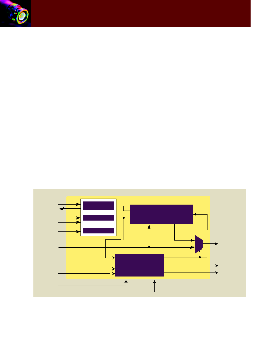
The encoders consist of 3 primary blocks as shown in Figure 2.
A section of storage is reserved for the generator polynomial
coefficients, the total number of symbols in the codeword
(codeword length), and the number of appended check
symbols (parity length). The codeword length and parity
length registers are written and read via standard processor
interface signals, as are the generator polynomial coefficients,
a series of stored constants covering the range of 0 to 20
appended parity symbols. The parity symbol calculation
block is responsible for producing the parity values from the
input data sequence and the generator polynomial
coefficients. The count and control circuitry performs internal
control operations and switches the output data stream
between the input information data stream and the generated
parity values.
Figure 2: CS3110/CS3112 Block Diagram
UP_Din
UP_ Dout
Codeword Generator
Coefficients
Parity Symbol Calculation
Data_Out
FStart_Out
Data_Valid_Out
Count and Control
FStart_In
Data_In
Data_Valid_In
Clk
Reset
Parity Length
Codeword Length
RD
WR
Add
3
TM
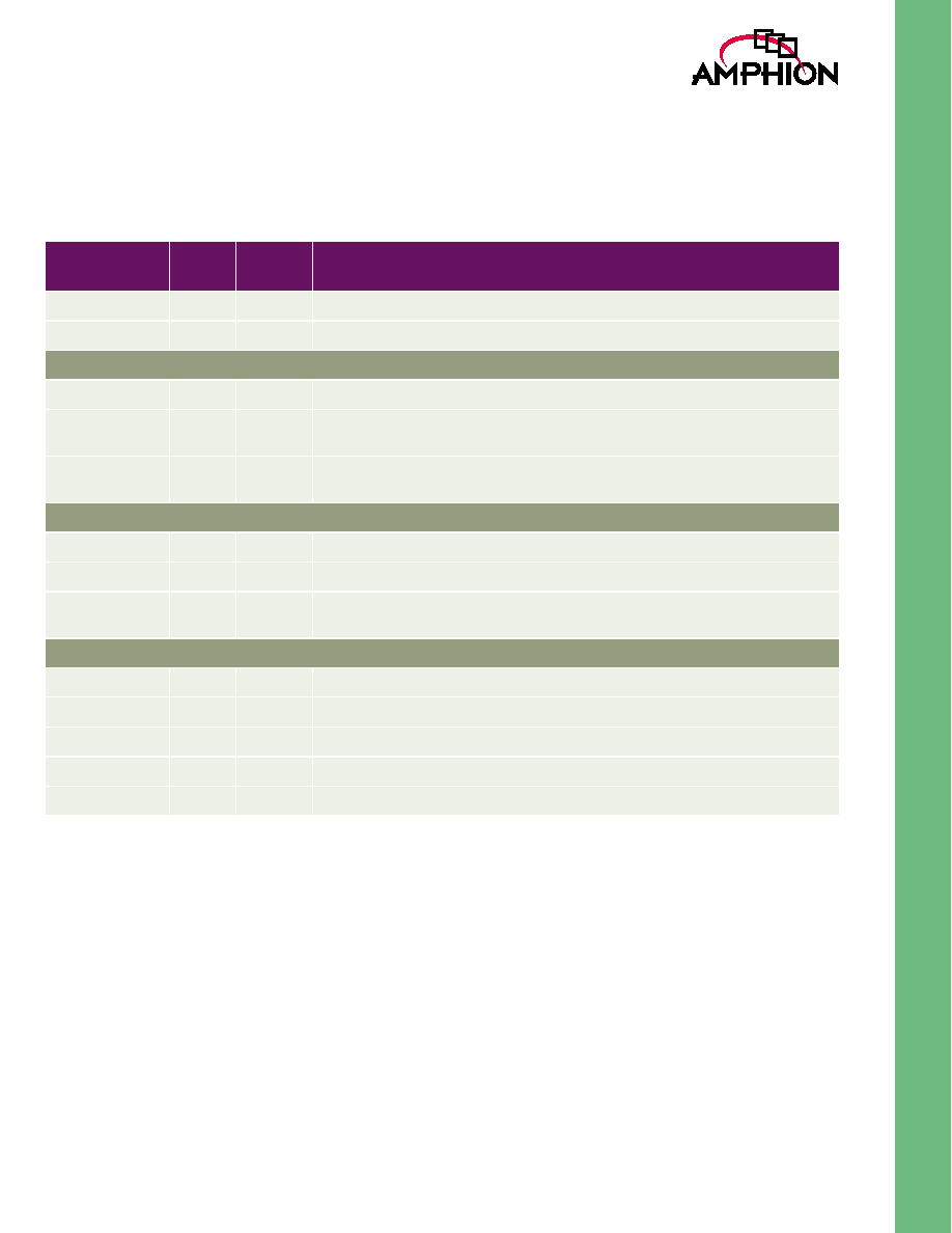
PIN/PORT DESCRIPTION
Table 1 gives the descriptions of the input and output ports of the CS3110 and CS3112 Reed Solomon encoders. Unless otherwise
stated, all signals are active high and bit (0) is the least significant bit.
Table 1: Input and Output Descriptions
SIGNAL
I/O
WIDTH
(Bits)
Description
CLK
I
1
Symbol rate clock, rising edge active
Reset
I
1
Asynchronous Master Reset, active high
Data Stream Input Port
Data_In [7:0]
I
8
Input data symbol, 8 bits wide
FStart_In
I
1
When high, indicates the data on Data_In is the first symbol in a new information
sequence
Data_Valid_In
I
1
When high signifies that the signals at the Data_In and FStart_In ports contain
valid information
Data Stream Output Port
Data_Out [7:0]
O
8
Output data symbol, 8 bits wide
FStart_Out
O
1
When high, indicates the data on Data_Out is the first symbol in a new coded block
Data_Valid_Out
O
1
When high, signifies that the signals at the Data_Out and FStart_Out ports contain
valid information
Control and Configuration
UP_Din [7:0]
I
18
Data Bus input from microprocessor
Add [4:0]
I
5
Address Bus from microprocessor
RD
I
1
Read Enable for Data Bus
WR
I
1
Write Enable for Data Bus
UP_Dout [7:0]
O
8
Data Bus output to microprocessor
4
CS3110/12
Reed-Solomon Encoders
PROCESSOR INTERFACE
Before operation of the encoder can commence, the code generator polynomial coefficients, the codeword length and the parity
length must be loaded into their appropriate registers via the processor interface. The addresses of the respective registers are
given in Table 2.
Addresses 00
HEX
� 13
HEX
contain the code generator
polynomial coefficients, while address 1F
HEX
contains the
codeword length value (in symbols) and address 1F
HEX
contains the parity length value. Every time the parity length
changes, its value and the values of the appropriate generator
coefficients must be loaded into their registers before error-
free encoding can commence. Values are loaded into their
respective registers by applying the correct address signal to
Add, the parameter values to UP_Din and then asserting the
write enable signal. The inputs Add and UP_Din are sampled
on the write signal WR rising edge. The contents of the
registers can be read by applying the correct address signal to
Add and asserting the read enable signal RD. The contents are
loaded to UP_Dout on the read signal RD rising edge.
RESET AND CLOCKING STRATEGY
All synchronous elements in the encoders are clocked using
the rising edge of the Clk signal. The exceptions to this are the
registers holding the generator polynomial coefficients,
codeword length and parity length. These are written and
read using strobe signals present in the processor interface.
Additionally, all I/O signals are registered on the rising edge
of Clk, with the exception of Reset. When the reset signal
Reset is asserted, all registers will be set to zero value. The
codeword length register will be loaded with the value FF
HEX
(255
10
) and the parity length register will be loaded with the
value 10
HEX
(16
10
). The code generator polynomial registers
are loaded with the corresponding coefficients for the given
parity length. The default code rate is therefore (255, 239).
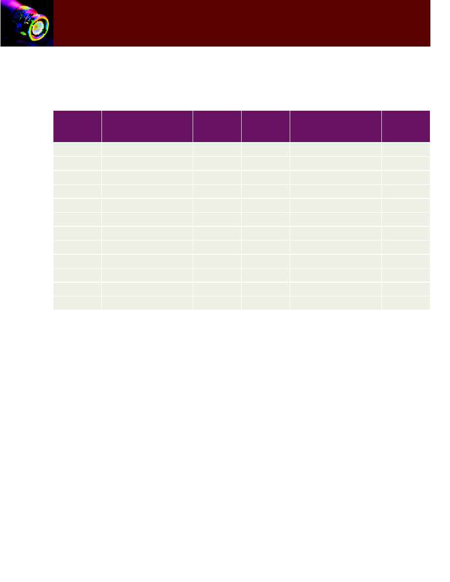
Table 2: Register Address Contents for Microprocessor Interface
ADDRESS
(HEX)
CONTENT
CONTENT
WIDTH
(bits)
ADDRESS
(HEX)
CONTENT
CONTENT
WIDTH
(bits)
00
Generator Coefficient (0)
8
OC
Generator Coefficient (12)
8
01
Generator Coefficient (1)
8
OD
Generator Coefficient (13)
8
02
Generator Coefficient (2)
8
OE
Generator Coefficient (14)
8
03
Generator Coefficient (3)
8
OF
Generator Coefficient (15)
8
04
Generator Coefficient (4)
8
10
Generator Coefficient (16)
8
05
Generator Coefficient (5)
8
11
Generator Coefficient (17)
8
06
Generator Coefficient (6)
8
12
Generator Coefficient (18)
8
07
Generator Coefficient (7)
8
13
Generator Coefficient (19)
8
08
Generator Coefficient (8)
8
14-1D
Reserved
x
09
Generator Coefficient (9)
8
1E
Codeword Length (symbols)
8
0A
Generator Coefficient (10)
8
1F
Parity Length (symbols)
5
0B
Generator Coefficient (11)
8
5
TM
INPUT DATA INTERFACE
The Data_Valid_In signal should be asserted whenever valid
data is present on Data_In and FStart_In. Data_Valid_In acts as
a clock enable and if de-asserted, the encoder will not sample
the signals at FStart_In and Data_In. Therefore, there is no
requirement for the information sequence to be input in a
continuous stream. If Data_Valid_In is de-asserted after a
complete information sequence has been input, the encoder
will continue to clock out the output parity values, despite the
fact that the input data flow has stalled.
FStart_In should be asserted for one clock cycle at the same
time as the first information symbol in a new sequence is
applied to Data_In, allowing the appropriate parameters to be
read. After k information symbols have been applied to the
encoder, Data_In will not be sampled for a further N � K clock
cycle, to allow the parity symbols to be output. The only
exception to this scheme occurs if FStart_In signal is asserted
at any time before a complete codeword has been output. In
this case the encoder will restart the encoding process with the
current value on Data_In as the start of a new information
sequence; and, output data values for the previous coded
block that have not yet emerged from the encoder will be lost.
If the values held in the generator polynomial coefficients,
codeword length and parity length registers are updated, the
updated register values are not applied until the next
assertion of FStart_In. Therefore, the programmable registers
can be updated while the encoder is still processing the
previous block. All programmable parameters must be stable
one clock cycle before the beginning of the new information
sequence to which the updated parameters should be applied.
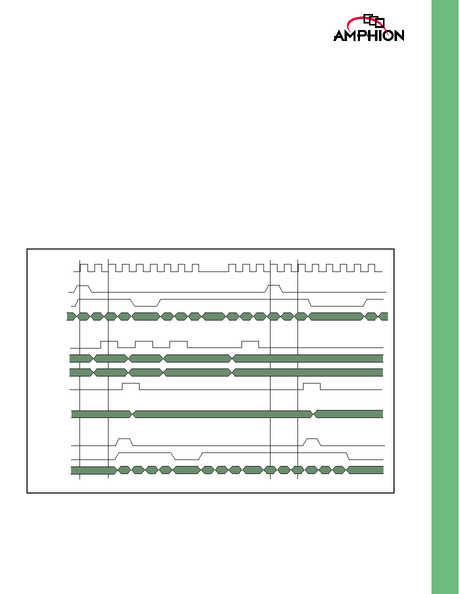
OUTPUT DATA INTERFACE
FStart_Out is asserted high for one clock cycle at the same
time as the first codeword symbol appears on Data_Out.
When valid information symbols are present on Data_Out, the
output Data_Valid_Out signal is asserted high.
Figure 3: Functional Timing Characteristics of the CS3110 and CS3112
CLK (I)
FStart_In
FStart_Out
Data_Valid_In
Symbol 0
Symbol 1
Symbol 3
Generator Coefficient #2
Generator Coefficient #3
Codeword Length
Codeword Length
Generator Coefficient #1
Generator Coefficient #1
Symbol 4
Symbol 0
Symbol 1
Symbol 3
Symbol 4
Symbol
n-2
Symbol
n-1
Symbol 0
Symbol
n-2
Symbol
n-1
Symbol 0
Data_In
Data_Valid_Out