 | –≠–ª–µ–∫—Ç—Ä–æ–Ω–Ω—ã–π –∫–æ–º–ø–æ–Ω–µ–Ω—Ç: CS3410AA | –°–∫–∞—á–∞—Ç—å:  PDF PDF  ZIP ZIP |

TM
Virtual Components for the Converging World
Amphion continues to expand its family of application-specific cores
1
See http://www.amphion.com for a current list of products
CS3410
High Speed Viterbi/TCM Decoder
The CS3410 Viterbi/TCM Decoder is a high performance implementation suitable for a range of Forward Error
Correction applications. This highly integrated Application Specific Virtual Component (ASVC) can be used in
conjunction with other FEC related cores available from Amphion to rapidly construct complete FEC solutions.
The Viterbi/TCM decoder operates in Viterbi or Trellis modes and provides a wide range of coding rates. The
CS3410 is available in both ASIC and programmable logic versions that have been hand crafted by Amphion to
deliver high performance while minimizing power consumption and silicon area.
Figure 1: Typical Transmission System Mode
Data In
CS3310
Convolutional
Encoder
Data Out
CS3410
Viterbi/TCM
Decoder
Noise
DECODER FEATURES
Viterbi/TCM decoder
-
Constraint length = 7
-
Traceback length = 170
Supports block and continuous mode
operations
Generator polynomials
-
G0 = 171 (octal)
-
G1 = 133 (octal)
-
G2 = 165 (octal) Viterbi mode
High coding gains at 10
-5
BER
5.6dB rate Viterbi
5.2dB rate Viterbi
3.3dB rate TCM
3.5dB rate TCM
Synchronization status monitoring
Microprocessor style interface for setup/
control and status monitoring
Automatic phase synchronization
"Force-to-Zero" mechanism (block mode)
Viterbi mode:
-
Fully compliant with:
INTELSAT IESS-308/ 309
DVB ETS 300-421
DVB-T ETSI 300-744
-
4-bit soft decision OR 1-bit hard decision
inputs
-
Coding rates:
1/2, 1/3 for QPSK
2/3, 3/4, 5/6, 7/8 obtainable via external
puncture control
-
BER monitoring
Trellis mode:
-
8-bit I/Q input (direct from demodulator)
-
Coding rates:
2/3 (8-PSK), 3/4 (16-PSK)
KEY METRICS
Size: 272K Gates (STD Cells)
Memory: 203K Gates
Logic area: 69K Gates
Input clock: 100 MHz
See Tables 7-8 for more details.
APPLICATIONS
Wireless LANs
Digital cellular phones
Satellite communications
1
3
---
1
3
---
1
2
---
2
3
---
3
4
---

2
CS3410
High Speed Viterbi/TCM Decoder
CS3410 SYMBOL AND
PIN DESCRIPTION
Table 1 provides the descriptions of the input and output
ports of the CS3410 Viterbi/TCM decoder (shown graphically
in Figure 2). Unless otherwise stated, all signals are active
high and bit(0) is the least significant bit.
Figure 2: CS3410 Symbol
R2ERASE
R1ERASE
R0ERASE
R1
R2
R0
Q
I
CLK
RESET
µ
P Interface
OSYNC
SYNCS
BERDONE
VITDATA
TCMDATA
DVALO
BLKSTARTO
BLKSTOPO
CHSYNC
BLKST
AR
TI
BLKST
OPI
DV
ALI
Sync
Status
WR
ADD
UP_DIN
UP_
DOUT
RD
BLKERR
SYNCUP
Table 1: CS3410 - Viterbi/TCM Decoder Interface Signal Definitions
Signal
I/O
Width (Bits)
Description
R0
I
4
Soft decision vector from demodulator (Viterbi mode)
R1
I
4
Soft decision vector from demodulator (Viterbi mode)
R2
I
4
Soft decision vector from demodulator (Viterbi mode ≠ rate 1/3)
R0ERASE
I
1
Erase flag (used to obtain external punctured codes in Viterbi mode) ≠ when active,
internal circuitry ignores R0 vector contribution during branch metric calculations.
R1ERASE
I
1
Erase flag (used to obtain external punctured codes in Viterbi mode) ≠ when active,
internal circuitry ignores R1 vector contribution during branch metric calculations.
R2ERASE
I
1
Erase flag (used to obtain external punctured codes in Viterbi mode) ≠ when active,
internal circuitry ignores R2 vector contribution during branch metric calculations
(Viterbi mode ≠ rate 1/3)
I
I
8
I vector direct from demodulator (TCM mode)
Q
I
8
Q vector direct from demodulator (TCM mode)
CLK
I
1
Clock
RESET
I
1
Asynchronous reset
CHSYNC
I
1
External synchronization control (see ADD8 register) ≠ rising edge sensitive.
BLKSTARTI
I
1
Start of block marker ≠ marks the first valid input data symbol
BLKSTOPI
I
1
End of block marker ≠ marks the last valid input data symbol
DVALI
I
1
Input data valid
SYNCS
O
1
Synchronization status: 0 indicates perfect synchronization; 1 indicates that input
data is rotated and synchronization is required - updated on SYNCUP.
OSYNC
O
1
`Out-of-sync' as a result of THRES comparison ≠ high if THRES is exceeded during
any test period. This signal indicates a loss of synchronization ≠ updated on SYN-
CUP (valid for one clock cycle).

3
TM
CONVOLUTIONAL CODES FOR ERROR
CORRECTION
Convolutional error-correction capabilities result from
outputs that depend on past data values. Each coded bit is
generated by convolving the input bit with the previous
uncoded bits. Convolving a signal with itself adds a level of
dependence on the past values. This mechanism provides the
ability to correct (to a certain level) a signal that has been
corrupted with noise such as Additive White Gaussian Noise
(AWGN).
Data that is convolutionally encoded can be decoded through
knowledge of the possible state transitions, created from the
dependence of the current symbol on past data. The allowable
state transitions are represented by a trellis diagram. Both the
Viterbi and TCM (Trellis Coded Modulation) decoder
functions supported by CS3410 utilize this principal.
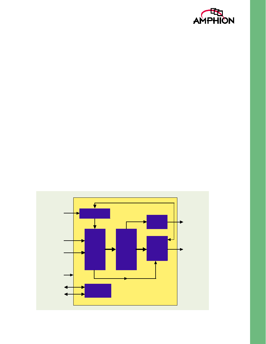
FUNCTIONAL DESCRIPTION
The CS3410 has been designed with high performance
applications in mind, e.g. DVB. The speed, error correcting
performance and flexibility of CS3410 makes it an all-round
contender for many FEC applications. The Viterbi mode is
typically used for systems that are power-limited but not
bandwidth-limited, whereas the TCM mode is typically used
for systems that are both power-limited and bandwidth-
limited. As a result, the CS3410 is well suited to many FEC
applications including satellite communication networks
(IMARSAT and INTELSAT IESS-308/9), microwave links and
modems. The following sections describe the main functional
blocks for CS3410 configured for Viterbi (Figure 3) or TCM
(Figure 4) decoding respectively. These blocks conceptually
describe the operation of the CS3410 in these two different
modes of operation.
VITERBI MODE
Input Data Interface
Input Data Interface block, formats and arranges data ready
for branch metric calculation. This includes a soft decision
"swap-and-invert" function as well as erasure tracking control
for punctured code rates, where certain bits of the encoded
data may be `punctured', or deleted, and not transmitted. At
the receiver, these punctured bits are replaced with null bits
prior to decoding with the rate 1/2 decoder. For punctured
operation, inserted null bits are marked using the RxERASE
input pins. The CS3410 supports signed magnitude or offset
binary formatted soft decision input vectors. Table 2 describes
these formats.
SYNCUP
O
1
Indicates synchronization update period ≠ valid for one clock cycle.
BLKERR
O
1
Indicates synchronization loss in block mode ≠ updated on SYNCUP
BERDONE
O
1
BER register updated (Viterbi mode only)
VITDATA
O
1
Viterbi Decoder output
TCMDATA
O
3
TCM decoder output
DVALO
O
1
Output data (decoded) valid
BLK-
STARTO
O
1
Start of block marker ≠ marks the first valid output bit(s) of a burst
BLKSTOPO
O
1
End of block marker ≠ marks the last valid output bit(s) of a burst
Microprocessor Interface
WR
I
1
Write strobe
RD
I
1
Read strobe
ADD
I
4
Address bus
UP_DIN
I
8
Input data
UP_DOUT
O
8
Output data
Table 1: CS3410 - Viterbi/TCM Decoder Interface Signal Definitions
Signal
I/O
Width (Bits)
Description

4
CS3410
High Speed Viterbi/TCM Decoder
Figure 3: Viterbi Decoder BLock Diagram
A hard decision mode of operation is also available in Viterbi
mode. In this case the input data bits must be connected to the
MSB of the Rx ports on the core.
Sync Control
Sync Control block provides a method to control/adjust the
phase synchronization of input soft decision vectors ("swap-
and-invert"). Used to eliminate
±90∞ phase ambiguities
introduced by QPSK demodulation.
BM Unit
This block is the Branch Metric calculator for Viterbi decoder.
When the RxERASE flags are active, the internal circuitry
ignores their vector contribution during branch metric
calculations.
Viterbi Decoder Core
This block is a 64-state Viterbi core and associated control and
memory units.
Input Data
Interface
Viterbi
Decoder
BM Unit
Differential
Decoder
Sync Control
Sync
Monitor
BER
Monitor
VITDATA
Sync Status
µP Interface
Status/Control
µP Interface
R2ERASE
R1ERASE
R0ERASE
R1
R2
R0
CLK
Sync Control
Table 2: Input Data Format (Viterbi Mode)
FSEL = 0
(Sign
Magnitude)
FSEL = 1
(Offset
Binary)
Value
1111
1111
Most confident +
1110
1110
(Data = 1)
1101
1101
1100
1100
1011
1011
1010
1010
1001
1001
1000
1000
Least confident +
0000
0111
Least confident -
0001
0110
0010
0101
0011
0100
0100
0011
0101
0010
0110
0001
(Data = 0)
0111
0000
Most confident -
Table 2: Input Data Format (Viterbi Mode)
FSEL = 0
(Sign
Magnitude)
FSEL = 1
(Offset
Binary)
Value
5
TM
Differential Decoder
Differential Decoder block is required to eliminate
±180∞
phase ambiguities introduced by QPSK demodulation
(assumes that input data to convolutional encoder has been
differentially encoded). A bypass mode is also available.
Sync Monitor
Synchronisation monitor indicates the phase synchronisation
status/error with respect to the input data vectors.
BER Monitor
Channel bit error rate estimation unit
µP Interface
Microprocessor interface facilitates the decoder setup/control
and status monitoring.
TCM MODE
Input Data Format
In TCM mode, input I/Q vectors must be provided in a signed
magnitude form.
TCM BM Unit
This unit provides the branch metric calculator and rotation
logic for TCM decoder. It computes branch metrics using 8-bit
signed magnitude formatted I/Q vectors. Branch metric
rotation is supported for 'out-of-sync' states thus eliminating
any ±
/4 (8-PSK) and ±
/8 (16-PSK) phase ambiguities that
may arise. A sector number which describes a receive point in
PSK space is generated for the PARD unit.
Sync Control
Provides a method to control/adjust the phase
synchronization of input I/Q vectors through the rotation of
branch metrics in the TCM BM unit.
Viterbi Decoder Core
This block is a 64-state Viterbi core and associated control and
memory units.
Differential Decoder/PARD
Differential Decoder and Phase Ambiguity Resolution
Decoder (PARD) are used to obtain TCM decoded bits
(includes a PARD pre-processor). A differential bypass mode
is also available.
Sync Monitor
Synchronization monitor indicates the phase synchronization
status/error with respect to the input data vectors.
µ
P Interface
Microprocessor interface facilitates the decoder setup/control
and status monitoring.
Figure 4: TCM Decoder Block Diagram
Viterbi
Decoder
TCM BM
Unit
+
BM
Rotation
Differential
Decoder/
PARD
Sync Control
Sync
Monitor
TCMDATA
Sync Status
µ
P Interface
Status/Control
µ
P Interface
Q
I
CLK
Sync Control