 | –≠–ª–µ–∫—Ç—Ä–æ–Ω–Ω—ã–π –∫–æ–º–ø–æ–Ω–µ–Ω—Ç: CS3411 | –°–∫–∞—á–∞—Ç—å:  PDF PDF  ZIP ZIP |
TM
Virtual Components for the Converging World
Amphion continues to expand its family of application-specific cores
1
See http://www.amphion.com for a current list of products
CS3411
High Speed Viterbi Decoder
The CS3411 Viterbi Decoder is a high performance implementation suitable for a range of Forward Error
Correction applications. This highly integrated application specific core can be used in conjunction with other
FEC related cores available from Amphion to rapidly construct complete FEC solutions. The Viterbi decoder
provides a wide range of coding rates and is available in both ASIC and programmable logic versions that have
been handcrafted by Amphion to deliver high performance while minimizing power consumption and silicon
area.
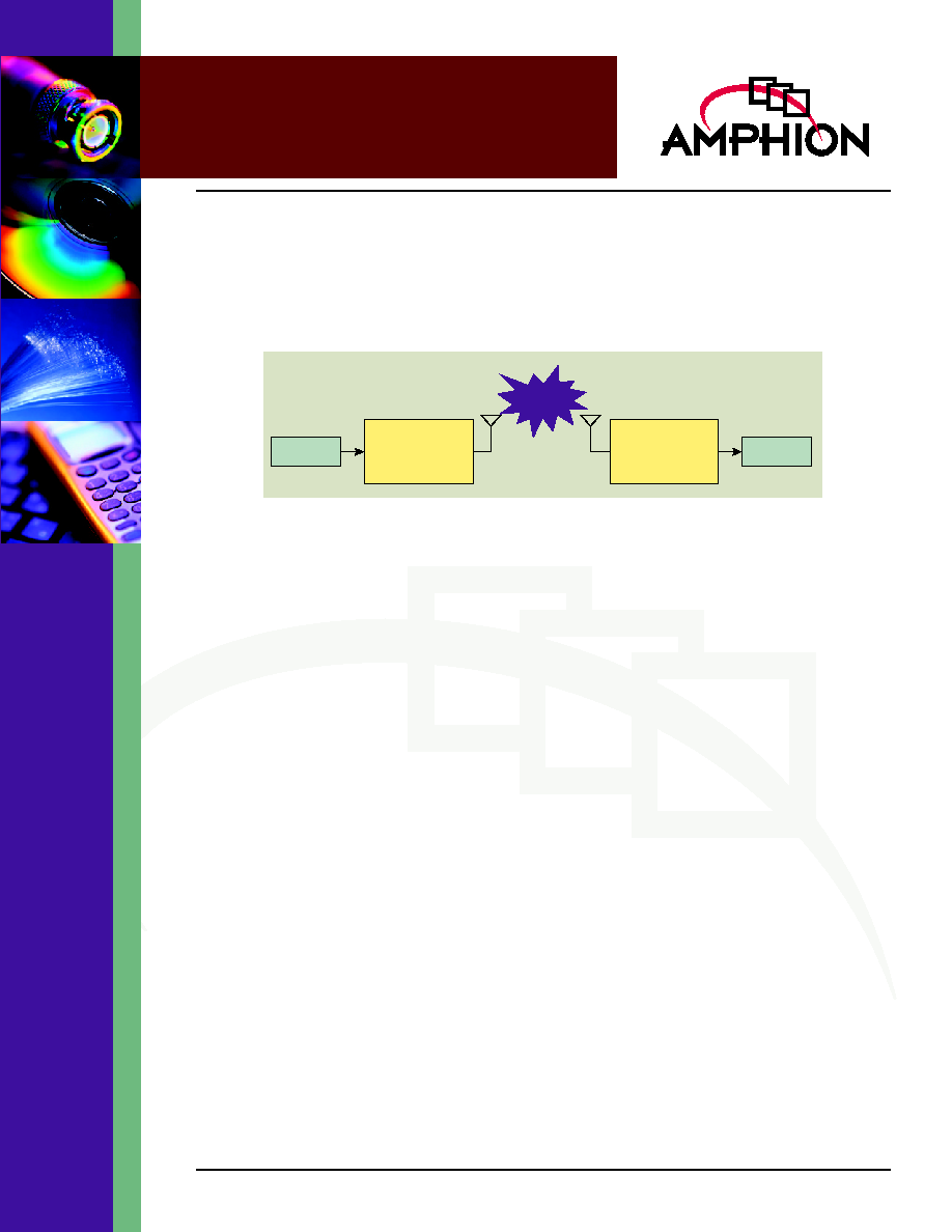
Figure 1: Typical Transmission System Model
Data In
CS3311
Convolutional
Encoder
Data Out
CS3411
Viterbi
Decoder
Noise
DECODER FEATURES
Fully compliant with INTELSAT IESS-308/ 309
Block mode operation
Constraint length = 7
Traceback length = 170
3-bit soft decision and 1-bit hard decision
inputs (4-bit I/Q inputs)
Coding rates up to 7/8 obtainable via external
puncture control
Generator Polynomials:
-
G0 = 171 (Octal)
-
G1 = 133 (Octal)
"Force-to-Zero" mechanism
High coding gains at BERs of 10
-5
KEY METRICS
Size:
208K Gates (STD Cells) - including
memory
Memory:
174K Gates equivalent
Logic area:
34K Gates
Input clock:
>100 MHz
See Tables 5-6 for more details.
APPLICATIONS
Wireless LANs
Digital cellular phones
Satellite communications
2
CS3411
High Speed Viterbi Decoder
CONVOLUTIONAL CODES FOR ERROR
CORRECTION
Convolutional error-correction capabilities result from
outputs that depend on past data values. Each coded bit is
generated by convolving the input bit with the previous
uncoded bits. Convolving a signal with itself adds a level of
dependence on the past values. This mechanism provides the
ability to correct (to a certain level) a signal that has been
corrupted with noise such as Additive White Gaussian Noise
(AWGN).
Data that is convolutionally encoded can be decoded through
knowledge of the possible state transitions, created from the
dependence of the current symbol on past data. The Viterbi
decoder functions supported by CS3411 utilize this principal.
FUNCTIONAL DESCRIPTION
The CS3411 has been designed with high performance
applications in mind. The speed, error correcting performance
and flexibility of the CS3411 makes it an all-round contender
for many FEC applications. The Viterbi decoder is typically
used for systems that are power-limited systems. As a result,
the CS3411 is well suited to many FEC applications including
satellite communication networks (IMARSAT and INTELSAT
IESS-308/9), microwave links, data storage and modems. The
following sections describe the main functional blocks for the
CS3411. A block diagram of the CS3411 is shown in Figure 2.
Figure 2: Viterbi Decoder Block Diagram
Viterbi
Decoder
BM Unit
BER
Monitor
Viterbi
Parameters
QERASE
IERASE
TPERIOD
Q
THRES
I
CLK
Input Data
Interface
Burst
Control
RESETN
BLKSTOPI
BLKSTARTI
BLKSTOPO
BLKSTARTO
DO
DVALID
BLKERR
BER
BPERIOD
3
TM
CS3411 SYMBOL AND
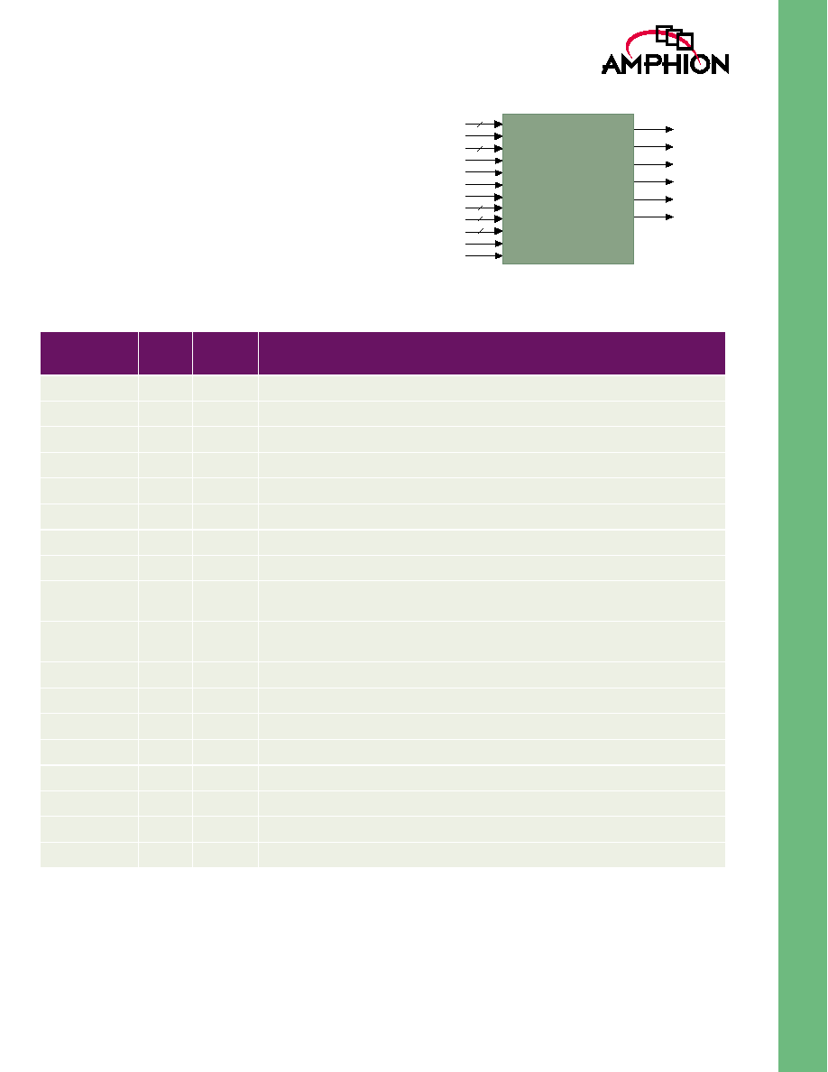
PIN DESCRIPTION
Table 1 describes the input and output ports (shown
graphically in Figure 3) of the CS3411 High Speed Viterbi
decoder. Unless otherwise stated, all signals are active high
and bit(0) is the least significant bit.
Figure 3: CS3411 Symbol
IQVALID
QERASE
IERASE
I[3:0]
Q[3:0]
BLKSTARTI
CLK
RESETN
DVALID
DO
BLKSTOPO
BER[15:0]
BLKERR
BLKSTARTO
CS3411
BLKSTOPI
TPERIOD{11:0}
THRES[11:0]
BPERIOD[15:0]
Table 1: CS3410 - Viterbi Decoder Interface Signal Definitions
Signal
I/O
Width
(Bits)
Description
I
I
4
I[3:0] - 4 bit I symbol (see Table 2 for definition)
IERASE
I
1
Active high I input symbol erase
Q
I
4
Q[3:0] - 4 bit Q symbol (see Table 2 for definition)
QERASE
I
1
Active high Q input symbol erase
IQVALID
I
1
Active high input symbol-pair/burst valid
BLKSTARTI
I
1
Active high start of burst marker - marks the first valid input symbol pair of a burst
BLKSTOPI
I
1
Active high end of burst marker - marks the last valid input symbol pair of a burst
THRES
I
12
Threshold setting used in generation of BLKERR
TPERIOD
I
12
Period count register. Sets count period over which metric normalizations will be
counted
BPERIOD
I
16
BER period count register. Sets count period over which BER measurement will take
place.
CLK
I
1
Clock input. Note: Clock is not related to data rate (hence requirement for DVALID)
RESETN
I
1
Active low, Asynchronous reset - resets decoder to known state
DO
O
1
Decoded serial output data valid
DVALID
O
Active high output data valid
BLKSTARTO
O
1
Active high start of burst marker - marks the first valid output bit of a burst
BLKSTOPO
O
1
Active high end of burst marker - marks the last valid output bit of a burst
BLKERR
O
1
Active high block error indicator
BER
O
16
Channel bit error rate measurement

4
CS3411
High Speed Viterbi Decoder
INPUT DATA INTERFACE
The input format for I and Q symbols is a sign-magnitude
format as defined in Table 2.
OPERATIONAL DESCRIPTION
A BLKERR event occurs when the rate of normalization is
exceeded, this being determined by the THRES value. To
obtain useful values of THRES, the normalization count (for a
single Viterbi trellis state) is observed with the decoder wired
in-sync and then out-of-sync configurations. Out-of-sync refers
to the I/Q inputs to the decoder that are rotated (±90∞) while
in-sync refers to the correct/direct connection of the I/Q ports
(0∞ rotation). Any value equal to or greater than THRES
indicates a block error (BLKERR). BLKERR is updated at the
end of the count period TPERIOD. The BLKERR register is
reset by BLKSTOPO (and RESETN). The THRES values in
Table 3 correspond to the "PathMetric Normalization" count
of a complete burst sequence that will trigger BLKERR - these
are example guidelines values. Note: A BLKERR cannot be
detected with ±180∞ rotated input I/Q vectors.
The internal circuitry will flag when a bit error occurs and the
bit error is counted over the period of an output burst. The
BER register gives an indication of the channel BER as it
contains the number of bit errors collected during a burst. It
should be noted that this circuitry is free running when
DVALID is active and is reset between bursts (BER is updated
every count period, i.e. TPERIOD). BLKSTOPI is used to
initiate the forcing of the metrics such that all survivor paths
go through the zero state between bursts. This requires that
the end of an encoder burst sequence contain at least 6 zero
bits.
The decoder has been designed to release valid output data as
soon as it is available. All survivor paths are forced through
the zero state and decisions can immediately be made on all
states prior to that. Therefore all the data up to this point will
be released from the traceback store on subsequent successive
clock cycles, regardless of the availability of valid symbols at
the input to the decoder.
TRACEBACK ARCHITECTURE AND
CORE LATENCY
The latency of the core is split into two categories dependant
upon burst length:
Bursts <= 340 bits, Latency = Burstlength + Burstlength/2+8
Bursts > 340 bits, Latency = 518 clocks
The burst processing nature of the decoder requires that there
be a minimum deadtime (in clock cycles) between bursts.
Bursts types/ranges can be categorized to describe this
deadtime. Burst ranges (length) are described by the equation
1. The minimum deadtime for each burst category (n) is
described in Table 4.
Table 2: CS3411 Data Input Interface
Indication
I/Q[3]
I/Q[2]
I/Q[1]
I/Q[0]
Strongest 1
1
1
1
1
1
1
1
0
1
1
0
0
1
0
1
1
1
0
1
0
1
0
0
1
Weakest 1
1
0
0
0
Weakest 0
0
0
0
0
0
0
1
0
0
1
0
0
0
1
1
0
1
0
0
0
1
0
1
0
1
1
0
Strongest 0
0
1
1
1
Table 3: Guideline THRES values for R=1/2 bursts
(Eb/N0 = 4.3, I/Q rotation 90
o
)
Burst length
TPERIOD
(base10)
THRES
(base 10)
56
55
6
180
179
17
360
359
39
792
791
73
1188
1187
103
2048
2047
180
n 170
◊
(
) 1
+
n 1
+
(
) 170
◊
where n ranges 0,.. [EQN 1]

5
TM
TIMING DIAGRAMS
Figure 4 and Figure 5 illustrate the functional timing diagrams
for the input and output signals of the CS3411. Figure 4
demonstrates the use of IQVALID, IERASE, QERASE,
BLKSTARTI and BLKSTOPI, whereas Figure 5 provides
similar information for DVALID, BLKERR, BLKSTARTO and
BLKSTOPO.
Note
: IERASE and QERASE could also be used for complete
symbol pair erasure as well as external depuncturing. Also
note that if DVALID is low then DO is low.
Figure 4: Input Timing Diagram
Figure 5: Output Timing Diagram
Table 4: Deadtime Burst Length Dependency
N
Burst range
(bits)
Deadtime
(clocks)
0
1 to 170
90
1, 2
171 to 510
260
3, 4, 5, 6,....
511 to
430
CLK
IQVALID
I[3:0]
IERASE
BLKSTARTI
BLKSTOPI
QERASE
Q[3:0]
CLK
DVALID
DO
BLKERR
BLKSTARTO
BLKSTOPO