 | –≠–ª–µ–∫—Ç—Ä–æ–Ω–Ω—ã–π –∫–æ–º–ø–æ–Ω–µ–Ω—Ç: CS3530TK | –°–∫–∞—á–∞—Ç—å:  PDF PDF  ZIP ZIP |
TM
Virtual Components for the Converging World
Amphion continues to expand its family of application-specific cores
1
See http://www.amphion.com for a current list of products
CS3530
Turbo Encoder
The CS3530 Turbo Encoder is designed to provide efficient and high performance solutions for a broad range of
applications requiring reliable communications in bandwidth scarce environments such as satellite and mobile
communications systems. This highly integrated application specific silicon core is fully compliant with 3GPP
and CDMA2000 standards. The CS3530 is available in both ASIC and FPGA versions that have been handcrafted
by Amphion for maximum performance while minimising power consumption and silicon area.
Figure 1: Turbo Encoder Overview Diagram
Interleaver
Encoder 2
Encoder 1
Puncture
Input
Output
FEATURES
Supports full range of W-CDMA and
CDMA2000 data block lengths and coding
rates
Throughput of 2.048 Mbps @ 30.72 MHz
clock
1
Simple processor interface allows easy
programming of configuration registers
Up to four different block length and coding
rate combinations can be pre-loaded into the
configuration registers, then switched within
a single cycle
Supports the production of coded output
symbols at the full clock rate.
Novel implementation of turbo interleaving
algorithm:
-
Continuous generation of interleaved address
sequence without stalls for invalid addresses
Core output can be stalled via external input
from downstream circuitry
All-synchronous design employing a single
clock, with exception of global asynchronous
reset
KEY METRICS
Logic Area:
20K gates
Core Memory:
4 Kbits (SP RAM)
Input Clock:
30.72
1
MHz
APPLICATIONS
3G cellular communications user equipment
3G cellular communications prototype and
test equipment
1. Max input clock can be scaled up to 200MHz in 180 nm technology and hence throughput increases.
2
CS3530
Turbo Encoder
TURBO CODES FOR ERROR CORRECTION
Turbo coding is a relatively recent development in the field of
Forward Error Correction. It permits reliable transmission of
data at rates approaching the theoretical capacity of a noisy
channel. Turbo codes are based on the use of several simple
encoders in the transmitter and decoders in the receiver,
arranged in a parallel or serial concatenation. Turbo codes
generally operate over blocks of data, with each constituent
encoder or decoder processing a differently-interleaved
version of the same data block. For 3rd generation (3G)
cellular systems, the specified configuration is two parallel
encoders or decoders, each employing an identical simple
convolutional code. The constituent code is systematic,
meaning that one of the coded output bits is identical to the
input data bit as shown in Figure 1.
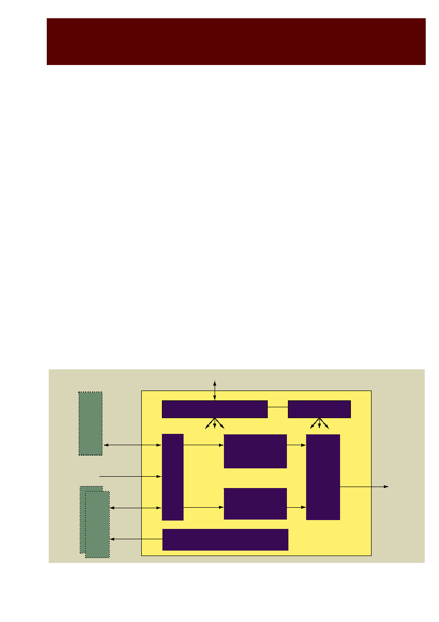
CS3530 FUNCTIONAL DESCRIPTION
The CS3530 Turbo Encoder is designed to provide an efficient
and high-performance solution for the turbo encoder
specifications supplied by the W-CDMA and CDMA2000
standards for 3rd generation cellular communications. It
supports all modes and configurations specified in the
aforementioned standards, and is capable of producing a
continuous encoded data stream at the full clock rate.
Parameters such as data Block Lengths, Coding Rates, etc. can
be written to and read from a series of configuration registers
within the core. A basic processor interface permits simple
access to these registers.
The CS3530 reads input data from two external synchronous
RAMs, one supplying the natural-order input data block to
the first convolutional encoder, and the second supplying the
interleaved data block to the second convolutional encoder.
By keeping these memories external to the core, system
designers have the option of sharing the memories with other
system functions not directly related to the turbo encoder.
Single-port memory is assumed for all large blocks of storage
in the ASIC architecture for reasons of power-efficiency. For
the FPGA architecture, the external storage may use memory
on or off the device.
Storage requirements for the systematic data vary depending
on whether the systematic memory is an independent
memory bank or a mapped region in a memory time-shared
between the turbo encoder and other system functions. In the
former case, a 4096x8 single-port RAM is required, while in
the latter case a memory region at least 2592x8 must be
reserved. Similar requirements exist for the interleaved data,
except two independent banks of 4096x8 single-port RAM, or
two independently accessible memory address regions sized
at least 2592x8 are required.
The following subsections provide brief, high-level
description of the internal blocks of the core shown in
Figure 2.
Figure 2: CS3530 Turbo Encoder Overview Diagram
Systematic
Storage
Interleaver
Storage
CS3530
µP Interface
Output Data
Input Data
Configuration Registers
Controller
Interleaved Address Generator
Convolutional
Encoder 1
Input Memory Interface
Puncture Unit
Convolutional
Encoder 2
3
TM
CONFIGURATION REGISTERS
The configuration registers are written to and read from a
simple processor interface. The registers hold the current
CS3530 configuration in terms of the 3G standard (W-CDMA
or CDMA2000), data block length and coding rate. The valid
values for the data block length and coding rate for W-CDMA
and CDMA2000 are shown in Table 1.
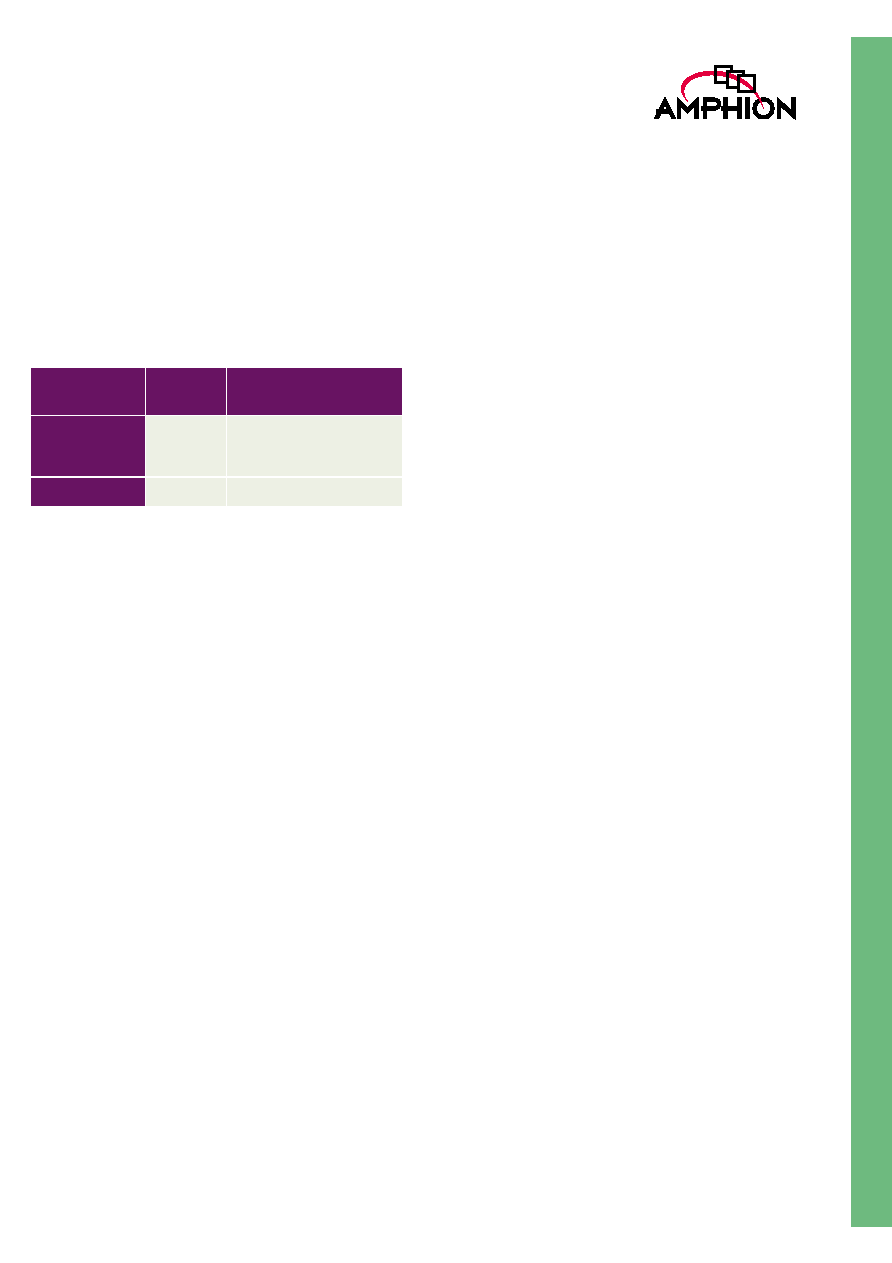
Please note that not all combinations of the CDMA2000 block
lengths and coding rates listed here are valid, and the reader is
referred to the appropriate standard for more information.
Four different data block length and coding rate combinations
can be pre-loaded into the configuration registers. These are
initially written to shadow registers, so that updated
parameters can be written while data processing continues
using the current four sets of parameters. A flag
(loadblklngth) to the core indicates when the contents of all
the shadow registers are transferred as a block into the
corresponding main registers. Selection between the four sets
of current parameters is carried out via another input signal
(swblklngth), and the next parameter set is switched in the
following cycle.
INPUT MEMORY INTERFACE
The CS3530 accepts a bit-serial stream of input data to be
encoded. This data is packed into 8-bit bytes, and written
concurrently to two external synchronous memories. Once the
entire data block has been written, data is read back out of the
storage. The systematic storage, when read back, supplies the
natural-order input data block to the first convolutional
encoder, and the interleaver storage supplies the interleaved
data block to the second convolutional encoder. Single-port
memory is assumed for all large blocks of storage in the ASIC
architecture, for reasons of power-efficiency. For the FPGA
architecture, the external storage may use the memory on or
off the device. Access to the input memories is byte-wide, and
allows continuous encoding at output coded symbol rates up
to the full clock rate. By keeping these memories external to
the core, system designers have the option of sharing the
memories with other system functions not directly related to
the turbo encoder.
By allowing the read interface to the systematic RAM to be
byte-wide, the number of individual memory accesses is
reduced, resulting in reduced power consumption. Since
encoding can be continuous at the full clock rate, writing a
block to systematic memory is overlapped with the reading of
the previous block from the RAMs. However, each byte write
or read only occurs every 8th cycle, hence a single time-shared
bank of single-port RAM can be used.
In compliance with the W-CDMA and CDMA2000 standards,
the interleave function is executed by writing a data block to
memory in natural order, and reading it using a pseudo-
random address sequence produced by a separate interleaved
address generation unit, discussed in a subsequent
subsection. The reader is referred to the applicable standards
documents for more details on the algorithm that calculates
the interleaved address sequence. Since writing is carried out
in natural order, byte-wide write access to the interleaver
RAM can again be carried out once every 8th cycle. Assuming
continuous data processing, the read interface to the
interleaver memory, which employs the pseudo-random
address sequence, can be active every cycle. The most
significant bits of the address provide the byte value, while
the 3 least significant bits are used to select which bit within
the byte is the next interleaved data value. The CS3530
supplies the complete address, and the selection of the
appropriate bit from the read byte is carried out externally to
the core.
CONTROLLER
The controller is responsible for the derivation of some global
control signals that are passed to the other modules, chiefly
enable and reset signals. It is also responsible for monitoring
the state of the encoder pipeline and issuing stall signals if
necessary. The use of the core input signal that stalls the
CS3530 output to downstream circuitry can cause data to
accumulate within the core and input memories. Additionally,
changing the data block length causes the interleaved address
generator unit to re-initialise, during which time data cannot
be read from the input memories to the core. This is explained
in greater detail in the subsequent subsection. The controller
monitors how full the input memories are, and the current
initialisation state of the interleaver, and flags to the upstream
circuitry when it is not possible for the core to accept further
input data bits.
Table 1: Valid BLock Length and Coding Rate for
W-CDMA and CDMA2000
W-
CDMA
CDMA2000
Block Length
40 to 5114
378, 570, 762, 1146, 1530,
2298, 3066, 4602, 6138,
9210, 12282, 20730
Coding Rate
1/3
1/2, 1/3, 1/4
4
CS3530
Turbo Encoder
INTERLEAVED ADDRESS GENERATOR
The interleaved address generator is responsible for
producing the pseudo-random address sequence for reading
the interleaver storage. The address generator can produce the
next value in the address sequence every clock cycle and can
bypass the production of invalid addresses. These two
features are inherent characteristics of the address generation
algorithms of both W-CDMA and CDMA2000. An invalid
address is defined as an address value equal to or exceeding
the data block length, assuming addressing begins from zero.
The interleaved address generator requires a certain
initialisation time between receiving an updated data block
length from the configuration registers, and production of the
first interleaved address value. The number of clock cycles
required for initialisation varies with the value of the new data
block length. However, the number of clock cycles required
for interleaver initialisation is always less than the value of the
new data block length. While the interleaver is initialising,
reading from the interleaver memory and systematic memory
is stalled. This situation only requires the stalling of input data
to the core if the writing to the input memories of a complete
block of data at the new block length completes before
interleaver initialisation to that new block length. If this
condition occurs, the core flags that the input data bit stream
should be temporarily stalled.
CONVOLUTIONAL ENCODER
Each constituent convolutional encoder is capable of encoding
data as specified in the 3G standards. The convolutional
encoder carries out an 8-state systematic recursive
convolutional code, with a transfer function of
where:
d(D) = 1 + D
2
+ D
3
n
0
(D) = 1 + D + D
3
n
1
(D) = 1 + D + D
3
(CDMA2000)
n
1
(D) = 0
(W-CDMA)
Therefore, the constituent convolutional encoder is rate 1/3 for
CDMA2000 and rate Ω for W-CDMA.
Since 3G turbo coding forces a block structure on the
convolutional code, a series of three tail bits needs to be driven
into the convolutional encoder after the input data sequence.
This forces the encoding trellis to terminate in a known state,
which is defined in the standards as state zero. The input tail
bits are formed by connecting the recursive feedback bit in the
encoder to the data input. During the three successive enabled
clock cycles, the three coded output tail values emerge. The
timing of the tail production is controlled by the controller
unit. The tail for the first convolutional encoder is produced
first, with the second encoder disabled. After this, the tail for
the second encoder is produced.
PUNCTURE UNIT
The puncture unit accepts the coded values from the two
convolutional encoders. Hence, for each turbo encoder input
bit, the puncture unit accepts 4 bits and produces 3 bits in the
case of W-CDMA, since the overall turbo encoding rate is
fixed at 1/3. An exception occurs when the W-CDMA turbo
encoder produces tail outputs, when only 2 coded bits are
retained for each input data bit. For CDMA2000, the puncture
unit accepts 6 bits and produces either 2, 3, or 4 bits,
depending on whether the selected overall coding rate is 1/2,
1/3 or 1/4. This is the case when processing both normal data
and tail inputs.
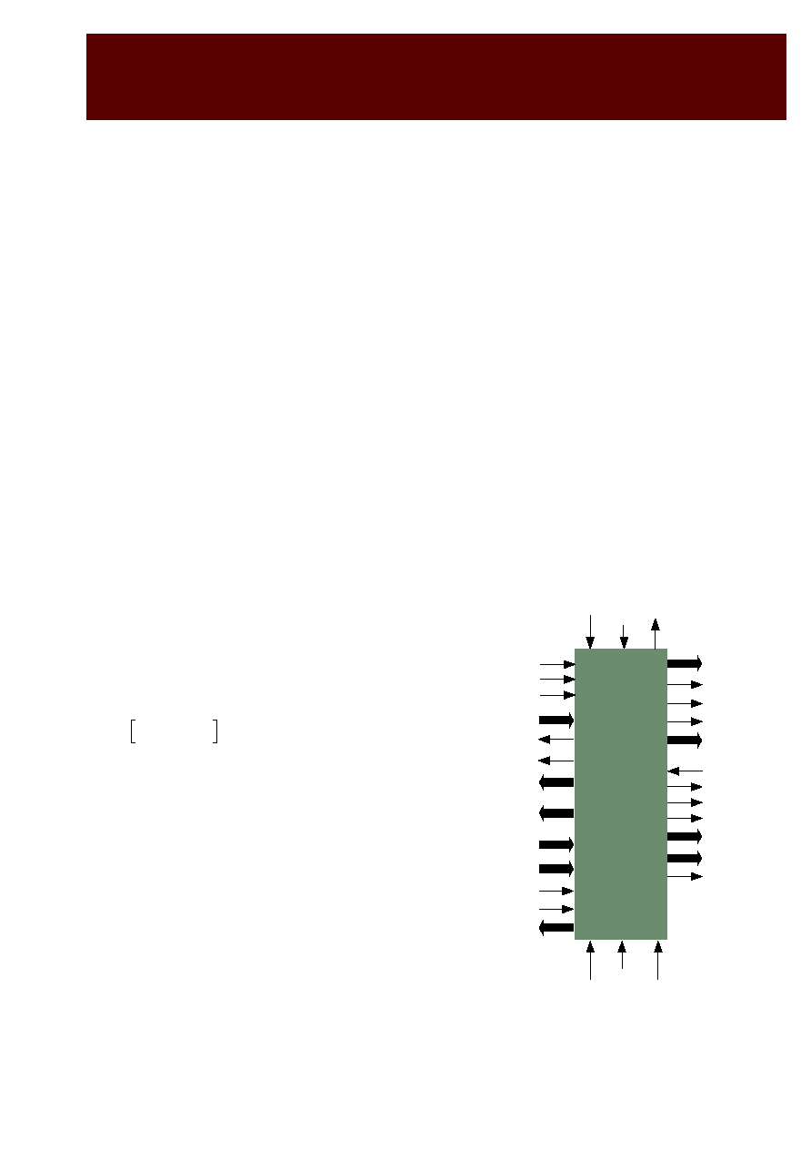
CS3530 SYMBOL
AND PIN DESCRIPTION
Table 2 describes the input and output ports (shown
graphically in Figure 3) of the CS3530 Turbo Encoder core.
Unless otherwise stated, all signals are active high and bit (0)
is the least significant bit.
Figure 3: CS3530 Symbol
G
D
1
n
0
D
( )
d D
( )
---------------
n
1
D
( )
d D
( )
---------------
=
CS3530
data_in
blkst_in
dvalid_in
sys_ram_out[7:0]
sys_ram_in[7:0]
sys_ram_csn
sys_ram_wrn_rd
sys_ram_add[11:0]
data_out[3:0]
blkst_out
blkend_out
dvalid_out
data_out_wth[1:0]
int_ram_in
int_ram_wcsn
int_ram_rcsn
int_ram_blksel
int_ram_wadd[11:0]
int_ram_radd[14:0]
int_ram_out[7:0]
up_din[15:0]
up_add[2:0]
up_csn
up_rd_wrn
up_dout[15:0]
loadblklngth
swblklngth
opbusy
clk
reset_n
encbusy

5
TM
Table 2: CS3530 I/O Definition
Signal
Width
(bits)
I/O
Description
Global Signals
clk
1
I
Clock rate must be at least the maximum short-term data rate, including
the overhead of the 6 tail symbols. All I/O (except reset_n) is assumed to
be synchronous to this clock. All sequential elements are clocked on the
rising edge of this signal.
reset_n
1
I
Global asynchronous reset, active low
Configuration Register Interface Signals
up_din
16
I
Data input port for microprocessor interface for access to configuration
registers. Data on this port is latched to the register addressed when the
chip select is active, and the read/write strobe selects a write operation.
up_add
3
I
Address port for the microprocessor interface to select configuration reg-
isters.
up_csn
1
I
Chip select strobe for the microprocessor interface to the configuration
registers ≠ active low.
up_wrn_rd
1
I
Read / write strobe for the microprocessor interface ≠ writes when low,
reads when high.
up_dout
16
O
Data output port for microprocessor interface for access to configuration
registers. Data from the addressed register is clocked out on this port
after the chip select is active, and the read/write strobe selects a read
operation.
loadblklngth
1
I
Input flag which is asserted when the set of block lengths and code rates
loaded via the microprocessor interface into the shadow registers should
be transferred into the corresponding main registers. It is asserted high
for 1 clock cycle during the last symbol of the last block using the current
block lengths
swblklngth
1
I
Input flag which is asserted when the next block length and code rate
combination from the set of 4 should be selected. It is asserted high for 1
clock cycle during the last data input of the last block using the old block
length and code rate combination. This cycle should also correspond to
dvalid_in being high for the last block input.
Data Input Signals
data_in
1
I
Input data bit. Data can be burst in at the full clock rate, but must be
stalled temporarily if the insertion of the tail symbols causes further data
input to be unacceptable.
blkst_in
1
I
When high, indicates the first input value in a turbo coding data block. It
is asserted one clock cycle before the first bit of a block is on the input
dvalid_in
1
I
When high, indicates valid data on data_in.
Data Output Signals
data_out
4
O
Data output. For CDMA2000, up to 4 output bits are produced for every
input bit (depending on coding rate), while for W-CDMA only the 3 least
significant bits of this output are valid.