 | –≠–ª–µ–∫—Ç—Ä–æ–Ω–Ω—ã–π –∫–æ–º–ø–æ–Ω–µ–Ω—Ç: CS3630 | –°–∫–∞—á–∞—Ç—å:  PDF PDF  ZIP ZIP |
TM
Virtual Components for the Converging World
Amphion continues to expand its family of application-specific cores
1
See http://www.amphion.com for a current list of products
CS3630
Turbo Decoder
The CS3630 Turbo Decoder is designed to provide efficient and high performance solutions for a broad range of
applications requiring reliable communications in bandwidth scarce environments such as satellite and mobile
communications systems. This highly integrated application specific silicon core is fully compliant with 3GPP
and CDMA2000 standards. The CS3630 is available in both ASIC and FPGA versions that have been handcrafted
by Amphion for maximum performance while minimising power consumption and silicon area.
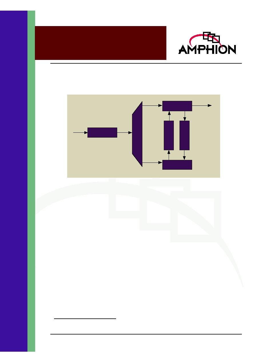
Figure 1: A Turbo Decoder Overview Diagram
Interleaver
Decoder 2
Decoder 1
De-puncture
Input
Output
De-interleaver
FEATURES
Supports full range of W-CDMA and
CDMA2000 data block lengths and coding
rates
Throughput of 2.048 Mbps (for 7 iterations) @
30.72
1
MHz clock
Up to four different block length and coding
rate combinations can be pre-loaded to the
configuration registers, then switched within
a single cycle
Power minimization features:
-
Early termination mechanism to prevent
unnecessary iterations
-
Max and min number of half-iterations can be
programmed into configuration registers
Novel implementation of turbo interleaving
algorithm
-
Continuous generation of interleaved address
sequence without stalls for invalid addresses
Efficient implementation of log-MAP SISO
decoding algorithm to provide:
-
Significant extra coding gain over the max-
log-MAP or SOVA
-
High error-correcting performance using a
small number of bits for internal decoder met-
rics to save silicon area and power
Simple processor interface for easy
programming of configuration registers
All-synchronous design using a single clock,
except for global asynchronous reset
KEY METRICS
Logic Area:
60K
Core Memory:
187 Kbits (SP RAM)
Input Clock:
30.72
1
MHz
APPLICATIONS
3G cellular communications user equipment
3G cellular communications base stations
3G cellular communications prototype and
test equipment
1. The Max clock can be scaled up to 150MHz hence the throughput and number of iterations increase.
2
CS3630
Turbo Decoder
TURBO CODES FOR ERROR CORRECTION
Turbo coding is a relatively recent development in the field of
Forward Error Correction. It permits reliable transmission of
data at rates approaching the theoretical capacity of a noisy
channel. Turbo codes are based on the use of several simple
encoders in the transmitter and decoders in the receiver,
arranged in a parallel or serial concatenation. Turbo codes
generally operate over blocks of data, with each constituent
encoder or decoder processing a differently-interleaved
version of the same data block. For 3rd generation (3G)
cellular systems, the specified configuration is two parallel
encoders or decoders, each employing an identical simple
convolutional code.
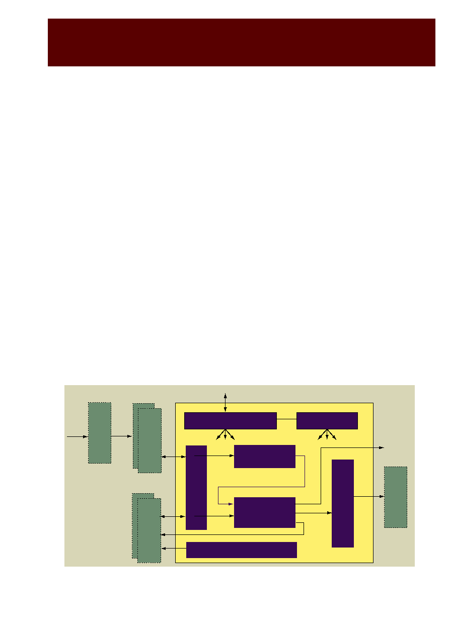
CS3630 FUNCTIONAL DESCRIPTION
The CS3630 Turbo Decoder is designed to provide an efficient
and high-performance solution for the turbo decoder
specifications supplied by the W-CDMA and CDMA2000
standards for 3rd generation cellular communications. It
supports all modes and configurations specified in the
aforementioned standards, and is capable of producing a
decoded data stream at a maximum average data rate of 2.048
Mbits/sec. Parameters such as data block lengths, coding rates,
etc. can be written to and read from a series of configuration
registers within the core. A basic processor interface permits
simple access to these registers. Figure 2, represents a
functional block diagram of the CS3630 Turbo decoder.
The CS3630 reads input data from, and writes the decoded
data to, external synchronous RAMs. Similarly, an additional
area of synchronous storage is used to hold soft output data
from the decoder for interleaving purposes. By keeping these
memories external to the core, system designers have the
option of sharing the memories with other system functions
not directly related to the turbo decoder. Single-port memory
is assumed for all large blocks of storage in the ASIC
architecture, for reasons of power-efficiency. For the FPGA
architecture, the external storage may use the memory on or
off the device.
Two independent banks of single-port RAM, each sized
20736x4, are required to hold input data for each soft input
value. Therefore, to support the CDMA2000 coding rate 1/4,
four sets of two banks are needed. This arrangement allows
independent access to each soft input value for power-saving
purposes, since concurrent access to all four soft input values
is not necessary. For the interleaver, two independent banks of
single-port RAM, each sized 20730x4, are required. The
requirement for multiple banks arises from the fact that new
input data can be written while turbo decoding is still being
carried out for the previous data block. Also, writing of new
soft output values to the interleaver can occur while reading
of old values from the opposite bank is still under way. For the
decoded output bit stream, one bank of single-port RAM,
sized 20730x1 is required. The lack of multiple banks for the
output data puts the responsibility on the system designer to
ensure decoded data blocks are completely read from storage
before the turbo decoder starts writing a new decoded
sequence.
The following subsections provide brief, high-level
descriptions of the internal blocks of the core shown in
Figure 2.
Figure 2: CS3630 Turbo Decoder Overview Diagram
Input Data
Storage
Interleaver
Storage
CS3630
µP Interface
Configuration Registers
Controller
De-puncture
Input Memory Interface
Output Memory Interface
MAP Decoder
Output Data
Statistics
Input Data
Pre-scaling
Output Data
Storage
Interleaved Address Generator

3
TM
DATA INPUT PRE-SCALING
Input data pre-scaling is actually carried out external to the
CS3630, but it is integral to achieving good performance from
the turbo decoder. Data scaling is a requirement for the log-
MAP algorithm to work correctly, and the value of the scaling
factor that multiplies the data is dependent on the current
state of the fading communications channel, and the levels of
additive noise. The level by which the turbo decoder input
data values should be scaled before application to the CS3630
is given by the expression a
k
x (2/
2
), where
2
is the variance
of the Additive White Gaussian Noise, and a
k
is the current
estimate of the faded signal amplitude at the receiver input.
By scaling the input data, the relative weighting of the data
received directly from the channel and the data re-circulated
within the turbo decoder between successive iterations is
varied, dependent on channel and noise conditions.
CONFIGURATION REGISTERS
The configuration registers are written to and read from a
simple processor interface. The registers hold the current
CS3630 configuration in terms of the 3G standard (W-CDMA
or CDMA2000), data block length, coding rate, maximum and
minimum number of half-iterations, and early termination
threshold. The valid values for the data block length and
coding rate for W-CDMA and CDMA2000 are shown in
Table 1.
Please note that not all combinations of the CDMA2000 block
lengths and coding rates listed here are valid, and the reader is
referred to the appropriate standard for more information.
Four different data block length and coding rate combinations
can be pre-loaded into the configuration registers. These are
initially written to shadow registers, so that updated
parameters can be written while data processing continues
using the current four sets of parameters. A flag to the core
indicates when the contents of all the shadow registers are
transferred as a block into the corresponding main registers.
Selection between the four sets of current parameters is
carried out via another input signal, and the next parameter
set is switched in the following cycle.
The registers holding the maximum and minimum number of
half-iterations provide the ability to program the CS3630 with
upper and lower bounds on the number of decoding half-
iterations. The term "half-iteration" implies a single pass of the
data through the MAP decoder. A complete turbo decoding
iteration consists of two half-iterations, one processing data in
natural order and the other in interleaved order. Iterative
decoding can terminate after either half-iteration in a
complete iteration, for maximal decoding efficiency. The
CS3630 will always complete the number of half-iterations
specified in the minimum half-iteration configuration register,
regardless of any other decoding termination mechanism. The
CS3630 will always terminate iterative decoding, and write
out the current estimate for the decoded data block, once the
number of half-iterations contained in the maximum half-
iteration configuration register have completed.
The value held in the early termination threshold register
forms part of the CS3630 early termination procedure. This
allows decoding iterations to stop once the magnitude of the
MAP decoder soft output value for every position in the data
block exceeds the threshold value held in the register. For data
blocks that have not been badly corrupted by the channel and
noise, completely successful decoding may be possible long
before the maximum number of half-iterations has been
reached. This situation is detected by the magnitudes of the
MAP decoder soft output values quickly becoming large.
Once this occurs, iterative decoding can cease and the
decoded data based on the current block of MAP decoder
outputs can be written to the output memory. By preventing
the execution of unnecessary decoding iterations, significant
power savings can be achieved. The early termination
threshold value must be carefully chosen according to the
channel and noise conditions. Too large a value will result in
unnecessary processing, while too small a value will result in
decoding stopping before all possible output bit errors have
been corrected.
INPUT MEMORY INTERFACE
The input memory interface is responsible for deriving control
signals for the input data and interleaver buffers, and
obtaining data from these blocks of storage. In order to initiate
decoding for a block of data, the following procedure should
be followed. Once a complete block of input data values has
been written to the input data storage, a core input signal is
set, and the data is burst into the CS3630 at the full clock rate,
under the control of the memory interface. At this point, a core
output signal will be asserted, indicating that the decoder is
currently busy, and decoding should not be initiated for any
successive data blocks until the decoder indicates it is no
longer busy.
Table 1: Valid Block Length and Coding Rate for
W-CDMA and CDMA2000
W-
CDMA
CDMA2000
Block Length
40 to 5114
378, 570, 762, 1146, 1530,
2298, 3066, 4602, 6138,
9210, 12282, 20730
Coding Rate
1/3
1/2, 1/3, 1/4

4
CS3630
Turbo Decoder
In compliance with the W-CDMA and CDMA2000 standards,
the interleave function between the first and second half-
iterations is executed by writing a block of MAP decoder
outputs to memory in natural order, and reading it back using
a pseudo-random address sequence produced by a separate
interleaved address generation unit, discussed in a
subsequent subsection. The reader is referred to the applicable
standards documents for more details on the algorithm that
calculates the interleaved address sequence. Similarly,
between the second half-iteration of iteration N and the first
half-iteration of iteration N+1, the MAP decoder outputs are
written in interleaved order and read in natural order,
effecting a de-interleave operation.
CONTROLLER
The controller is responsible for the derivation of some global
control signals that are passed to the other modules, chiefly
enable and reset signals. It also has responsibility for
monitoring the number of half-iterations performed by the
decoder, and invocation of the early termination procedure.
INTERLEAVED ADDRESS GENERATOR
The interleaved address generator is responsible for
producing the pseudo-random address sequence for reading
the interleaver storage. The address generator can produce the
next value in the address sequence every clock cycle and can
bypass the production of invalid addresses. These two
features are inherent characteristics of the address generation
algorithms of both W-CDMA and CDMA2000. An invalid
address is defined as an address value equal to or exceeding
the data block length, assuming addressing begins from zero.
The interleaved address generator requires a certain
initialisation time between receiving an updated data block
length from the configuration registers, and production of the
first interleaved address value. The number of clock cycles
required for initialisation varies with the value of the new data
block length. However, the number of clock cycles required
for interleaver initialisation is always less than the value of the
new data block length. Since the interleaved address sequence
is not required until the start of the second half-iteration of
turbo decoding, re-initialisation of the interleaver does not
necessitate any additional stalling of decoder input data.
DE-PUNCTURE UNIT
De-puncturing is carried out on the decoder input data stream
before application to the MAP decoder inputs, as specified in
the 3G standards. De-punctured locations have null (zero)
values inserted at those positions in the data stream.
MAP DECODER
The MAP decoder is the decoding engine of the design, and is
responsible for carrying out the SOVA log-MAP algorithm. It
accepts input data from the channel, together with
information from the previous half-iteration, and produces a
sequence of soft output values that represent updated
estimates of the bit values in the data block. The
corresponding "hard" decoded bit for each soft output is
simply the sign bit of the soft output. The CS3630 uses 2's
complement number format exclusively.
The CS3630 uses a single MAP decoder, time-shared between
the two half-iterations associated with a full turbo decoding
iteration. The minimum clock rate of 30.72 MHz is sufficient to
allow this silicon-efficient architecture to maintain an average
decoded data rate of 2.048 Mbits/sec while carrying out 7
complete turbo decoding iterations. The MAP decoder, in
conjunction with the controller block, produces output
statistics for each decoded data block. It reports on the
number of half-iterations executed during the decoding of the
block, and whether decoding terminated as a result of the
early termination procedure. The CS3630 also calculates a
block reliability metric, which is an estimate of the reliability
of the complete decoded data block, based on the perceived
reliability of all the decoder decisions on each individual
decoded bit.
OUTPUT MEMORY INTERFACE
Once the CS3630 has determined that iterative turbo decoding
is complete for the current data block, the block of the
decoded bits is written to the output data memory under the
control of the output memory interface. The CS3630 only
provides control signals for the writing to this memory. It is
the responsibility of the system designer to ensure that
reading from this memory is carried out appropriately.

5
TM
CS3630 SYMBOL
AND PIN DESCRIPTION
Table 2 describes the input and output ports (shown
graphically in Figure 3) of the CS3630 Turbo Decoder core.
Unless otherwise stated, all signals are active high and bit (0)
is the least significant bit.
Figure 3: CS3630 Symbol
CS3630
blk_rdy
ipb_ram_in[15:0]
do_ram_csn
data_out
et_pass
hiter_done[4:0]
int_ram_in[3:0]
int_ram_wcsn
int_ram_rcsn
int_ram_blksel
int_ram_wadd[14:0]
int_ram_radd[14:0]
int_ram_out[3:0]
up_din[15:0]
up_add[3:0]
up_csn
up_wrn_rd
up_dout[15:0]
loadblklngth
swblklngth
clk
reset_n
dec_busy
do_ram_wadd[14:0]
blk_rel[3:0]
ipb_ram_csn[3:0]
ipb_ram_blksel
ipb_ram_radd[14:0]
Table 2: CS3630 Turbo Decoder Interface Signal Definition
Signal
Width
(bits)
I/O
Description
Global Signals
clk
1
I
Clock rate must be at least 30.72 MHz to support 7 full turbo decoding iterations at an
average user rate of 2.048 Mbits/sec. All I/O (except reset_n) is assumed to be synchro-
nous to this clock. All sequential elements are clocked on the rising edge of this signal.
reset_n
1
I
Global asynchronous reset, active low
Configuration Register Interface Signals
up_din
16
I
Data input port for microprocessor interface for access to configuration registers. Data
on this port is latched to the register addressed when the chip select is active, and the
read/write strobe selects a write operation.
up_add
4
I
Address port for the microprocessor interface to select configuration registers.
up_csn
1
I
Chip select strobe for the microprocessor interface to the configuration registers ≠ active
low.
up_wrn_rd
1
I
Read / write strobe for the microprocessor interface ≠ writes when low, reads when high.
up_dout
16
O
Data output port for microprocessor interface for access to configuration registers. Data
from the addressed register is clocked out on this port after the chip select is active, and
the read/write strobe selects a read operation.

6
CS3630
Turbo Decoder
loadblklngth
1
I
Input flag which is asserted when the set of block lengths and code rates loaded via the
microprocessor interface into the shadow registers should be transferred into the corre-
sponding main registers. It is asserted high for 1 clock cycle during the last symbol of the
last block using the current block lengths
swblklngth
1
I
Input flag which is asserted when the next block length and code rate combination from
the set of 4 should be selected. It is asserted high for 1 clock cycle during the last data
input of the last block using the old block length and code rate combination. This cycle
should also correspond to dvalid_in being high for the last block input.
Input Data Interface Signals
blk_rdy
1
I
Input flag which is asserted for a single cycle when a complete block of input data has
been written to the input data memory. Used as a "start decoding" flag by the CS3630.
Note that the dec_busy output is asserted once decoding has begun. Any attempt to re-
assert blk_rdy before dec_busy has been de-asserted from the previous data block will
be ignored by the core.
ipb_ram_in
16
I
Although depicted as a 16-bit bus, ipb_ram_in is really the concatenation of 4 streams of
4-bit soft input values read from independent storage regions (one for each soft value,
up to the 4 values implied by CDMA2000 rate
1
/
4
).
For each 4-bit soft value, the levels 1001 (-7) to 0111 (+7) are used to represent the most
confident 1 and the most confident 0 respectively. This implies that the value 1000 (-8) is
not used for valid data representation, and that 0000 represents a perfect null value. The
CS3630 treats a value of -8 as an unknown value, and replaces it with a value of 0. This
behavior is useful for 3GPP systems, where de-punctured locations from 3GPP rate
matching can be flagged to the CS3630 by setting the de-punctured data locations to a
value of -8.
ipb_ram_csn
4
O
Vector of 4 active-low chip selects for the 4 independent storage regions holding the soft
input data values. Since the CS3630 only controls the read interface of the storage,
these signals can also be considered as read enables.
ipb_ram_blksel
1
O
Each input data storage region contains 2 banks of single-port RAM. When
ipb_ram_blksel is low, reading should occur from bank 0, when high reading should
occur from bank 1.
ipb_ram_radd
15
O
Input data storage read address. Shared by all 4 independent storage regions.
Interleaver Storage Interface
int_ram_in
1
I
Data input bit from external RAM used for interleaving. The memory address for the
byte-wide storage is given by the top 12 bits of int_ram_radd. The 3 least significant bits
of int_ram_radd should be used to select the appropriate data input bit from the read
byte. Bit-to-byte packing is most significant bit first. Hence, if the 3 least significant bits of
int_ram_radd are 0, bit 7 of the byte value should be selected.
int_ram_wadd
12
O
Interleaver RAM write address. Bytes are written to the interleaver storage in natural
order.
int_ram_radd
15
O
Interleaver RAM read address. Produced in the interleaved address order via the inter-
leaved address generation unit in the core.
int_ram_wcsn
1
O
Chip select for interleaver RAM write accesses ≠ active low.
int_ram_rcsn
1
O
Chip select for interleaver RAM read accesses ≠ active low. Since the interleaver stor-
age comprises 2 independent banks of single-port memory (one reading and one writ-
ing), int_ram_rcsn and int_ram_wcsn are normally applied to opposite banks.
Table 2: CS3630 Turbo Decoder Interface Signal Definition
Signal
Width
(bits)
I/O
Description

7
TM
CONFIGURATION REGISTER ADDRESS MAP
The CS3630 uses a simple processor interface to write to and
read from the configuration registers. Configuration
parameters include the 3G standard used (W-CDMA or
CDMA2000), minimum and maximum number of half-
iterations, early termination threshold, and four sets of data
block length and coding rate combinations that can be
switched between using the input signal swblklngth. Updated
values for the four sets can be written to the core while data
processing with the current values of the four sets is ongoing.
This is possible because the updated values are initially
written to sets of shadow registers, which are loaded as a
complete block into the corresponding main registers using
the input signal loadblklngth.
The microprocessor interface consists of 16-bit data input and
output ports, 3-bit address bus, chip select and a read/write
strobe. The register address mapping is shown in Table 3.
int_ram_blksel
1
O
Interleaver RAM block. Selects between interleaver storage banks. Low when data
writes should be applied to bank 0, high when data writes should be applied to bank 1.
int_ram_out
4
O
Output data value from the MAP decoder to the interleaver RAM.
Output Data Interface SIgnals
data_out
1
O
Decoded output data bit.
do_ram_csn
1
O
Chip select for output RAM write access - active low
do_ram_wadd
15
O
Write address for output RAM
Output Data Statistics SIgnals
hiter_done
5
O
Number of half-iterations executed on the block of data just decoded. Values range from
0 to 31, although 14 is the upper limit for a sustained average data rate of 2.048 Mbits/
sec. However, for lower data rates, or when a previous block has decoded using rela-
tively few half-iterations, it is possible to raise the maximum number of iterations tempo-
rarily.
The value of hiter_done is updated 1 cycle after the last decoded bit value in the block
has been written to the output data storage
blk_rel
4
O
Block reliability value. Unsigned quantity ranging from 0 to 15. Larger values indicate
greater probability that the complete block has been decoded successfully.
The value of blk_rel is updated 1 cycle after the last decoded bit value in the block has
been written to the output data storage.
et_pass
1
O
Early termination pass indicator. If the block just decoded terminated as a result of the
early termination procedure, this signal goes high for 1 cycle after the last decoded bit
value in the block has been written to the output data storage.
Core Busy SIgnals
dec_busy
1
O
Decoder busy flag - active high. Asserted immediately after blk_rdy triggers the start of
decoding. De-asserted immediately after the decoded block is written to output storage.
Table 2: CS3630 Turbo Decoder Interface Signal Definition
Signal
Width
(bits)
I/O
Description

8
CS3630
Turbo Decoder
It should be noted that the state of the configuration registers after the core asynchronous reset has been activated corresponds to
the W-CDMA standard, with all block lengths set to 3856. The minimum number of iterations defaults to zero, and the maximum
number to 14. The early termination threshold is set to its most conservative value of 15. When reading configuration register
values, it is the value held in the main register that is placed on up_dout, not the current shadow register value.
Table 3: CS3630 Configuration Register Map
Address
Read/
Write
Default Value
(after reset)
Shadowed
Description
0000
R/W
3856 (base 10)
Y
First block length. Written and read using the 15 least sig-
nificant bits of up_din and up_dout, other unused.
0001
R/W
3856 (base 10)
Y
Second block length. Written and read using the 15 least
significant bits of up_din and up_dout, other unused.
0010
R/W
3856 (base 10)
Y
Third block length. Written and read using the 15 least
significant bits of up_din and up_dout, other unused.
0011
R/W
3856 (base 10)
Y
Fourth block length. Written and read using the 15 least
significant bits of up_din and up_dout, other unused.
0100
R/W
1
N
3G standard
0 = CDMA2000
1 = W-CDMA
0101
R/W
85 (base 10)
01010101 (base 2)
Y
Coding rates for the four block length parameters. Written
and read using the 8 least significant bits of up_din and
up_dout, others unused.
Bits [1:0] - code rate for block length 1
Bits [3:2] - code rate for block length 2
Bits [5:4] - code rate for block length 3
Bits [7:6] - code rate for block length 4
Each 2-bit coding rate identifier can take the following val-
ues
00 - rate 1/2
01 - rate 1/3
10 - rate 1/4
11 - unused
0110
R/W
14 (base 10)
N
Maximum number of half-iterations to be applied to each
data block. Written and read using the 5 least significant
bits of up_din and up_dout, others unused.
0111
R/W
0
N
Minimum number of half-iterations to be applied to each
data block. Written and read using the 5 least significant
bits of up_din and up_dout, others unused.
1000
R/W
15 (base 10)
N
Early termination threshold value. Early termination is
activated when the magnitude of all MAP decoder output
values in a block exceed this threshold. Written and read
using the 4 least significant bits of up_din and up_dout,
others unused.

9
TM
TIMING DIAGRAMS
This section provides an overview of data flow on the interfaces of the CS3630 during configuration register access, and normal
data processing.
CONFIGURATION REGISTER WRITE AND READ TIMING
This section provides an overview of data flow on the interfaces of the CS3630 during configuration register access, and normal
data processing.
The diagram in Figure 4 shows the setting up of the configuration registers with the four data block lengths bl1, bl2, bl3, and bl4
for W-CDMA. The maximum and minimum number of half-iterations is set to 14 and 2 respectively, and the early termination
threshold is 10. After writing the parameters, loadblklngth is asserted to transfer the values from shadow to main registers. At
some later time, the value in the register at address zero is read out.
Figure 4: Configuration Register Access Timing Diagram
clk
up_csn
up_wrn_rd
up_din
up_add
loadblklngth
up_dout
bl2
bl4
bl3
1
85
14
2
10
bl1
0
1
2
3
4
5
6
7
8
0
bl1

10
CS3630
Turbo Decoder
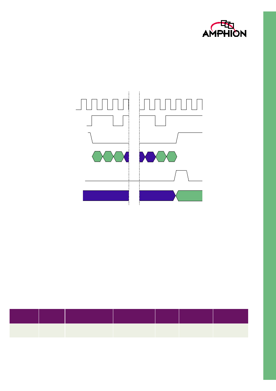
INPUT DATA TIMING
The diagram in Figure 5 shows the core input timing. After blk_rdy has been asserted for one cycle, the input buffer storage read
control signals are activated. The appropriate elements within the 4-bit ipb_ram_csn bus go low to activate the appropriate input
data storage regions. The value of ipb_ram_blksel toggles to select the appropriate bank of storage to read from. Note that the data
values read from the storage lag the address by a cycle, since the external storage has a synchronous read cycle.
Figure 5: Input Timing Diagram
0
1
2
bl-2
bl-1
0
1
clk
blk_rdy
ipb_ram_csn
ipb_ram_radd
ipb_ram_blksel
ipb_ram_in
D0
D1
D2
BLOCK N
BLOCK N+1
11
TM
OUTPUT DATA TIMING
The diagram in Figure 6 shows the core output timing. When the CS3630 decides that iterative decoding is complete, it writes the
decoded block continuously into the output data storage. The signal do_ram_csn goes active (low) while this is occurring.
Assuming the data block length is bl, the address sequence do_ram_wadd is either in natural order, assuming decoding terminates
after an odd number of half-iterations, or in the interleaved order for block length bl, assuming decoding terminates after an even
number of half-iterations. Immediately after the complete decoded block has been written to the output storage, the statistics
signals et_pass, blk_rel and hiter_done change to reflect the statistics of the data block just decoded.
Figure 6: Output Data Timing Diagram
AVAILABILITY AND IMPLEMENTATION INFORMATION
ASIC CORES
For applications that require the high performance, low cost and high integration of an ASIC, Amphion delivers application
specific silicon cores that are pre-optimized to a targeted silicon technology by Amphion experts.
Consult your local Amphion representative for product specific performance information, current availability of individual
products, and lead times on ASIC core porting.
*Performance figures based on silicon vendor design kit information. ASIC design is pre-layout using vendor-provided statistical wire loading information, under the
following condition: (T
J
= 125∫C, V
cc
-10%)
**Logic gates do not include clock circuitry
clk
data_out
do_ram_csn
do_ram_wadd
et_pass
hiter_done
blk_rel
A0
A1
A2
Abl-1
Table 4: CS3630 ASIC Core
PRODUCT
ID#
SILICON
VENDOR
PROCESS
PERFORMANCE*
(MBits/SEC)
LOGIC
GATES**
MEMORY
AREA
AVAILABILITY
CS3630TK
TSMC
180 nm using Artisan
standard Cell libraries
2.048
60K
187 Kbits single
port RAM
Now

CS3630
Turbo Decoder
TM
Virtual Components for the Converging World
CORPORATE HEADQUARTERS
Amphion Semiconductor Ltd
50 Malone Road
Belfast BT9 5BS
Northern Ireland, UK
Tel:
+44 28 9050 4000
Fax:
+44 28 9050 4001
EUROPEAN SALES
Amphion Semiconductor Ltd
CBXII, West Wing
382-390 Midsummer Boulevard
Central Milton Keynes
MK9 2RG England, UK
Tel:
+44 1908 847109
Fax:
+44 1908 847580
WORLDWIDE SALES & MARKETING
Amphion Semiconductor, Inc
2001 Gateway Place, Suite 130W
San Jose, CA 95110
Tel:
(408) 441 1248
Fax: (408)
441
1239
CANADA & EAST COAST US SALES
Amphion Semiconductor, Inc
Montreal
Quebec
Canada
Tel:
(450) 455 5544
Fax: (450)
455
5543
Web: www.amphion.com
Email: info@amphion.com
ABOUT AMPHION
Amphion (formerly Integrated
Silicon Systems) is the leading
supplier of speech coding, video/
image processing and channel
coding application specific silicon
cores for system-on-a-chip (SoC)
solutions in the broadband,
wireless, and mulitmedia markets
© 2002 Amphion Semiconductor Ltd. All rights reserved.
Amphion, the Amphion logo,"Virtual Components for the Converging World", are trademarks of Amphion Semiconductor Ltd. All others are the property of their
respective owners.
12
05/02 Publication #: DS3630v1.0
SALES AGENTS
SPS-DA PTE LTD
21 Science Park Rd
#03-19 The Aquarius
Singapore Science P ark II
Singapore 117628
T el:
+65 774 9070
Fax:
+65 774 9071
SPINNAKER SYSTEMS INC
Hatchobori SF Bldg. 5F 3-12-8
Hatchobori, Chuo-ku
T oky o 104-0033 Japan
Tel:
+81 3 3551 2275
Fax:
+81 3 3351 2614
V oy ageur T echnical Sales Inc
1 Rue Holiday
T our Est, Suite 501
P oint Claire, Quebec
Canada H9R 5N3
T el:
(905) 672 0361
Fax:
(905) 677 4986
JASONTECH, INC
Hansang Building, Suite 300
Bangyidong 181-3, Songpaku
Seoul Korea 138-050
T el:
+82 2 420 6700
Fax:
+82 2 420 8600
Phoenix T echnologies Ltd
3 Gavish Street
Kfar -Saba, 44424
Israel
T el:
+972 9 7644 800
Fax:
+972 9 7644 801