 | –≠–ª–µ–∫—Ç—Ä–æ–Ω–Ω—ã–π –∫–æ–º–ø–æ–Ω–µ–Ω—Ç: CS3810 | –°–∫–∞—á–∞—Ç—å:  PDF PDF  ZIP ZIP |
TM
Virtual Components for the Converging World
Amphion continues to expand its family of application-specific cores
1
See http://www.amphion.com for a current list of products
CS3810
32 QAM Demodulator
The CS3810 32 QAM broadband wireless demodulator core has been developed to provide an efficient and
highly optimized solution for wireless data networks. Combined with the CS3710 32 QAM modulator core data
transmission speeds of up to 155Mbps can be achieved at low error rates. The CS3810 is suited for applications
areas such as point-to-point WLAN, metropolitan area networks, wireless VPN and is easily combined with the
CS5200 series of AES cryptography cores to create secure high speed data links.
The CS3810 provides an integrated high performance complete baseband demodulation solution for wireless
data transmission. It includes symbol and timing recovery, adaptive filtering and precise lock tracking to ensure
optimal data recovery under adverse channel conditions. This includes signalling to control AGC and ADC,
ensuring straight forward system integration and deployment. A combined block synchronisation scheme and
error control/ correction system is included to deliver reliable data recovery. The core also includes a
straightforward microprocessor interface allowing the setting of demodulation parameters and easy system
integration.
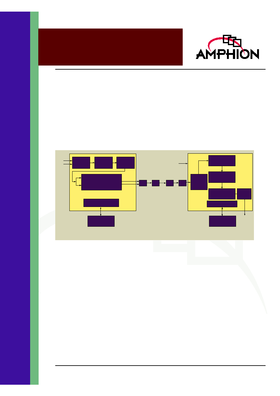
Figure 1: Block Diagram of CS3710/CS3810 Broadband Wireless Modulation/Demodulation Cores
Data
Encoding
Error
Protection
Mapping
Spectral Shaping
Control Registers
TXI_OUT
TXQ_OUT
Data Input
Test Input
Controller/
Processor
CS3710 Broadband Wireless Modulator Core
ADC
Timing/symbol
recovery
Decode &
Synchronisation
Error Correction
& Recovery
Control Registers
Filtering
Controller/
Processor
Test Input
Data Out
CS3810 Broadband Wireless Demodulator Core
Output
formatter
RF
RF
DAC
FEATURES
Fully integrated Digital Baseband
demodulator including timing and symbol
recovery and error correction
All digital timing and carrier recovery
Wide carrier tracking range
Acquisition time < 10ms.
Internal DC offset removal
I/Q imbalance adjustment
Programmable equalization adaptation rate
Residual BER better than 10
-12
Internal FIFO for smooth data output
Programmable carrier recovery loop
constants and damping factor
Equalizer weights read/write-able from
microprocessor bus
Forward Error Correction Features
Low FEC overhead
Concatenated RS-Convolutional interleaved
system
Interleaver employing the Intelsat method,
with depth of 4
Soft decision based Viterbi decoder, of
constraint length K=7 (64 states)
Input and output start of frame signals
Internal RS correction and Viterbi re-
normalization counters
Data Framing
Intelsat Style Frame/Superframe structure
Superframe detection output sync signals

2
CS3810
32 QAM Demodulator
APPLICATIONS
Wireless Metropolitan Area Network
Wireless LAN
Secure wireless VPN
Broadband voice, data and video transmission
INPUT/OUTPUT DESCRIPTION
Table 1 describes the input and output ports (shown
graphically in Figure 2) of the CS3810 demodulator core. All
the static programming signals can be overwritten by the
microprocessor interface except for ZIFMT that is set only by
the pin connection. Unless otherwise stated, all control signals
and input data are clocked in and all the outputs are clocked
out on the rising edge of the 74MHz clock signal (CLK), and
all control signals are active high.
The overall architecture of the demodulator core is illustrated
in Figure 3.
Figure 2: CS3810 Symbol
Figure 3: Block Diagram of the CS3810
RXUSRCLK
CLK
RESET
RESTART
ZIFMT
ZA
ZB
AGCREF
VCORNG
HBWBLL
FFKBLL
LCKTHBLL
LCKWINBLL
INIPCLL
AFCCLL
NAFCCLL
PILBWCLL
DDLBWCLL
MUCMAEQ
MUDDEQ
MapI
MapQ
MapStrb
Map Test
CS3810
Broadband
Wireless
Demodulator
RXSYNC
RXDATA
AGCP
VCSTRB
VCOV
AGCOK
AGCOK
LCKBLL
LCKCLL
STATCLL
FIFOERR
LCKTCM
LCKTUW
TCMERR
RSERR)U
RSERR_L
BLLSTRB
BLLIQ
BLLQI
DATA ADDR ALE CSB WRB OEB
RSERRPRD BYPASS UPTCM
16
5
8
12
3
16
16
16
11
11
11
Output
Data
VCO
control
Lock
Status
Stats
Test
Data
AGC
control
Global
control
P interface
Input
data
AGC
setting
BLL
settings
CLL
settings
FEC settings
10
10
8
2
2
2
2
4
4
8
2
Input
Data
Carrier
&
Symbol
Recovery
Phase
Lock &
Stream
Decode
Block
Synchron
-ization
Error
Correction
Descram-
bling
Deframing
Formatting
Output
Filtering
Control Register Bank
Symbol and Timing Recovery Core
(BLL/CLL)
FEC Decoder Core
Table 1: CS3810 32 QAM Demodulator Interface Signal Descriptions
Name
I/O
Width
Description
GLOBAL CONTROLS
CLK
Input
1
Input clock signal, generated by VCO and phase locked to the sampling
clock. Samples are clocked in and out on the rising edge
RXUSRCLK
Input
1
Output clock signal. Samples are clocked out of the demodulator FIFO
on the rising edge
RESET
Input
1
Asynchronous reset, active LOW

3
TM
RESTART
Input
1
Synchronous reset signal, active HIGH. The BLL restart the acquisition
process after it is activated. The CLL returns to idle state after RESTART
and re-starts acquisition until the BLL lock is achieved.
INPUT DATA
ZIFMT
Input
1
Input sample format, static programming signal
0: two's complement
1: offset binary
ZA
Input
10
Input sample A from DAC, 2x symbol rate (74MHz), format is determined
by ZIFMT
ZB
Input
10
Input sample B from DAC, 2x symbol rate (74MHz), format is determined
by ZIFMT
AGC SETTING
AGCREF
Input
8
AGC threshold reference, static programming signal
BLL SETTINGS
VCORNG
Input
1
VCO frequency range selection, static programming signal, specifying
the corresponding Df/f0 of the VCO when the 12-bit control signal VCOV
changes from the middle to the maximal or minimal value
0: 1/8192
1: 1/4092
The actual Df/f0 of the VCO may not be necessarily accurate as the
specified and the BLL can still be functioning. It only affects the BLL
acquisition range and speed.
HBWBLL
Input
1
Costas low pass filter H(f) gain factor selection, static programming sig-
nal
0: 1/32
1: 1/16
FFKBLL
Input
2
Frequency error low pass filter gain factor selection before the BLL lock
is declared, static programming signal
00: 1/2048
01: 1/1024
10: 1/512
11: 1/256
LFFKBLL
Input
2
Frequency error low pass filter gain factor selection, after the BLL lock is
declared, static programming signal
00: 1/16384
01: 1/8192
10: 1/4096
11: 1/2048
LCKTHBLL
Input
1
BLL Lock threshold selection, relative to the lock indicator value for ideal
signal, static programming signal
0: 1/2
1: æ
LCKWINBLL
Input
1
BLL lock detection window size selection, in terms of number of 32-QAM
symbols, static programming signal
0: 16384
1: 32768
Table 1: CS3810 32 QAM Demodulator Interface Signal Descriptions
Name
I/O
Width
Description

4
CS3810
32 QAM Demodulator
CLL SETTINGS
INIPCLL
Input
1
CLL initial period selection, in terms of 32-QAM symbols, static program-
ming signal,
0: 16384
1: 32768
When the BLL lock is declared, the CLL switches from idle state to initial
state in which the equalizer is put into CMA mode. The CLL acquisition
starts after the initial period.
AFCCLL
Input
1
Use or not use AFC for frequency offset estimate, static programming
signal
0: do not use AFC
1: use AFC
When AFC is not in use, the CLL uses a scan counter mechanism to
estimate the frequency offset. Every time when the pull-in fails the
counter is increased by one to give a new frequency offset value until the
lock is achieved.
NAFCCLL
Input
1
Number of AFC computations for averaging in AFC period
0: 16
1: 64
Simulation shows that in noisy conditions selection of 64 gives more reli-
able frequency offset estimate
PILBWCLL
Input
1
CLL pull-in (acquisition) mode bandwidth select
0: 0.0015(55KHz)
1: 0.003(110KHz)
The bandwidth is approximated based on the assumption of damping
factor of 0.71
DDLBWCLL
Input
1
CLL decision-direct (tracking) mode bandwidth select
0: 0.01(370KHz)
1: 0.02(740KHz)
The bandwidth is approximated based on the assumption of damping
factor of 0.71
MUCMAEQ
Input
2
Equalizer m select for CMA mode
00: 1/1024
01: 1/512
10: 1/256
11: 1/128
MUDDEQ
Input
2
Equalizer m select for DD LMS mode
00: 1/8192
01: 1/4096
10: 1/2048
11: 1/1024
OUTPUT DATA
RXSYNC
Output
1
Output ready flag. Signals that valid output data is present at the
RXDATA port
RXDATA
Output
8
Received output data port
Table 1: CS3810 32 QAM Demodulator Interface Signal Descriptions
Name
I/O
Width
Description

5
TM
ERROR CORRECTION STATISTICS
TCMERR
Output
16
Reports the number of estimated errors in the decoded IQ datastream
RSERR_U
Output
16
Reports the number of errors corrected by the Reed Solomon Decoder
(upper 16 bits)
RSERR_L
Output
16
Reports the number of errors corrected by the Reed Solomon Decoder
(lower 16 bits)
AGC CONTROL
AGCP
Output
1
AGC width-modulated pulse with period of 256 symbols. The pulse width
is proportional to the input signal level.
VCO CONTROL
VCOV
Output
12
VCO control voltage, 12-bit offset-binary format, normalized according to
the VCO frequency range such that the maximal value corresponds to
the lowest frequency and zero corresponds to the highest frequency,
updated every four symbols (9.25 MHz, 8 clock cycles)
VCSTRB
Output
1
VCO control voltage strobe, asserted for 4 cycles in every 8 clock cycles
to indicate the update of VCOV
ERROR CORRECTION CONTROL
RSERRPRD
Input
2
Static signal-sets the duration over which RS statistics are gathered
UPTCM
Input
8
Static signal used to control operation of TCM decoder
BYPASS
Input
1
Static signal, when asserted the TCM decoder is bypassed
LOCK STATUS
AGCOK
Output
1
AGC OK indicator, asserted when the average peak sample level is
within +/-15% of the ideal level
LCKBLL
Output
1
BLL lock flag, asserted when lock is declared or retained, updated once
every BLL lock detection window
LCKCLL
Output
1
CLL lock flag, asserted when lock is declared or retained, updated for
every output symbol (two clock cycles)
STATCLL
Output
3
CLL status, updated for every output symbol (two clock cycles)
000: idle (equalizer in initial mode, phase error set to 0)
001: initial (equalizer in CMA, phase error set to 0)
010: AFC (equalizer in CMA, estimate frequency offset)
011: DFS (equalizer in CMA, scan counter increases)
100: 4GC pull-in (equalizer in CMA, CLL 4GC pull-in)
110: DD pull-in (equalizer in CMA, CLL DD pull-in)
111: Lock (equalizer in DD, CLL DD tracking)
FIFOERROR
Output
1
When Asserted signifies the output fifo has overflowed and data has
been dropped
LCKTCM
Output
1
When asserted signifies the TCM decoder has achieved lock
LCKUW
Output
1
When asserted signifies that block synchronization has been achieved
Table 1: CS3810 32 QAM Demodulator Interface Signal Descriptions
Name
I/O
Width
Description

6
CS3810
32 QAM Demodulator
TEST DATA
BLLSTRB
Output
1
BLL output sample strobe, one cycle pulse every two clock cycles, indi-
cating the peak or transition samples after BLL lock is achieved
1: peak sample
0: transition sample
BLLIQ
Output
11
BLL output sample I, two's complement format
BLLQI
Output
11
BLL output sample Q, two's complement format
MAPI
Input
4
TCM decoder test input
MAPQ
Input
4
TCM decoder test input
MapStrb
Input
1
Active strobe signal used to sample MAPI and MAPQ
MapTest
Input
1
Static signal, when asserted MAPI and MAPQ are sampled otherwise
the demodulated data is decoded as normal
MICROPROCESSOR INTERFACE
DATA
Tri-state
16
16-bit data bus
ADDR
Input
5
5-bit address bus
ALE
Input
1
Address latch enable
CSB
Input
1
Chip select, level sensitive and active LOW
WRB
Input
1
Write/Read control signal
0: Write
1: Read
OEB
Input
1
Output enable, level sensitive and active LOW.
The demodulator drives the data bus only when both CSB and OEB are
active
Table 1: CS3810 32 QAM Demodulator Interface Signal Descriptions
Name
I/O
Width
Description

7
TM
DEMODULATOR OVERVIEW
The input to the demodulator may be fed directly from an A/
D converter. It samples the received spectrum at double the
symbol rate.
AGC
An AGC loop is implemented with an external gain control
element in order to achieve the desired receiver dynamic
range and maintain proper input level to the ADC. The AGC
module determines the average power of the input signal and
compares it to a programmed threshold. A pulse width
modulated signal is output by the AGC module. The PWM
stream is externally integrated and can be used as a AGC
control voltage.
TIMING RECOVERY
The received data stream then enters the symbol timing
recovery loop, which consists of resampling circuitry and
filtering, crosstalk removal, IQ imbalance adjustment and a
Digital Phase Locked Loop (DPLL). A combined resampling /
matched filter is used to enable transfer of the input data
stream from the input data domain to the symbol rate domain.
CARRIER RECOVERY
The recovered symbol rate data then enters the carrier
recovery loop of the demodulator. This consists of a de-
rotation module, removal of DC crosstalk, adjustment of any
I/Q imbalance, equalization and the DPLL. As the
constellation of the recovered symbol rate data can still be
rotating at this stage it is necessary to de-rotate this prior to
equalization.
After de-rotation the symbol rate data is applied to an
adaptive equaliser to remove transmission related distortions.
TCM
The recovered symbols are fed to the 64 state TCM decoder.
The user can select the puncture rate, lock thresholds or even
to bypass the TCM decoder. The TCM decoder provides BER
estimates which may be read via the microprocessor interface.
REED SOLOMON DECODING
Prior to RS decoding the block boundaries are recovered. The
sync detection circuitry searches for a unique word similar to
the scheme employed by Intelsat IESS-308. Once locked the
sync detection module also repacks the TCM output stream
into 8 bit Reed Solomon symbols.
The delineated blocks are de-interleaved and Reed Solomon
decoded. The corrected errors are reported and reflected on
the RSERR_U and RSERR_L output ports during a statistics
gathering period.
DESCRAMBLING
A self synchronizing descrambler utilizing a 2
20
-1 pattern
operates on the data stream thus de randomizing it to recover
the original modulated input message. Data from the
descrambler is written to a FIFO on the symbol rate clock and
output on RXDATA on the rising edge of the RXUSRCLK.
LOCK INDICATION
A number of lock indicators are provided as status registers
bits to enable the overall synchronisation status of the
demodulator to be monitored. These are:
∑
Symbol timing recovery loop lock
∑
Carrier recovery loop lock
∑
TCM decoder synchronized
∑
Unique word sync detection lock

8
CS3810
32 QAM Demodulator
TIMING CHARACTERISTICS
The programming signals are assumed to be static, i.e., they
do not change during normal operation process. The
microprocessor interface signals have been described in the
previous section. The timing diagrams of the other signals are
provided below, with reference to the clock and output
sample strobe signals.
Figure 4: Input Data Timing
Figure 5: AGC Control Timing
Figure 6: Test Data Timing
CLK
ZA
ZB
CLK
AGCP
AGCOK
ZSTRB
512 cycles (256 symbols)
CLK
BLLIQ
BLLQI
BLLSTRB

9
TM
PERFORMANCE
Figure 7 demonstrates the over all error correction performance of the Concatenated correction system employed by the decoder
(under AWGN conditions).
Figure 7: Error Correction Performance
The demodulator. acquisition performance is presented in shown in Table 2
BER Performance
1.00E-08
1.00E-07
1.00E-06
1.00E-05
1.00E-04
1.00E-03
1.00E-02
1.00E-01
1.00E+00
10
10.25
10.5
10.75
11
Eb/No (dB)
BE
R
Concatenated coded
data
Uncoded Data
Table 2: Demodulator Acquisition Performance
Metric
Performance
Carrier acquisition range
± 600KHz
Symbol acquisition range
>
± 140ppm of baud rate
Carrier tracking range
± 600KHz
Typical acquisition time
< 10 mS

10
CS3810
32 QAM Demodulator
PERFORMANCE AND DENSITY METRICS
PROGRAMMABLE LOGIC CORES - DENSITY METRICS
For ASIC prototyping or for projects requiring fast time-to-market of a programmable logic solution, Amphion programmable
logic cores offer the silicon-aware performance tuning found in all Amphion products, combined with the rapid design times
offered by today's leading programmable logic solutions.
The following performance and density metrics has been obtained when the demodulator core is implemented as a stand-alone
design in the device specified below. It should be noted that if the function is implemented on different FPGA devices, or
combined with additional logic in larger devices, then additional constraints might need to be applied to achieve the similar
metrics.
Note that the metrics are provided for demodulation (Table 3) and channel decoding (Table 4) separately.
Table 3: CS3810 FEC Decoder Programmable Logic Core - Altera
DEVICE
SILICON
VENDOR
AREA
MEMORY REQUIREMENT
CRITICAL PATH
(TXUSRXLK)
CRITICAL PATH
(CLK74M)
APEX20KC-7
Altera
10044 LEs
34 ESBs
56.82 MHz
(17.6 ns)
75.76 MHz
(13.2 ns)
Table 4: CS3810 Symbol & Timing Recovery Programmable Logic Core - Altera
DEVICE
SILICON
VENDOR
AREA
MEMORY REQUIREMENT
CRITICAL PATH
(CLK74M)
APEX20KC-7
Altera
11276 LEs
24 ESBs
74.63 MHz
(13.4 ns)

11
TM
Figure 8: Design Data Formats Supplied by Amphion
Data Formats
Supplied by AMPHION
Typical ASIC or FPGA Design Flow
(Conceptual)
Bit Accurate
C Model
RTL Simulation
Models
Testbench
(VHDL & Verilog)
Netlists
(Verilog, VHDL, EDIF, .bd)
FPGA Programming
Files
System-Level "C" Code simulation
Hardware RTL Development
RTL Simulation
Logic Synthesis
Gate-level analysis
(timing & functional)
Physical Design

CS3810
32 QAM Demodulator
TM
Virtual Components for the Converging World
CORPORATE HEADQUARTERS
Amphion Semiconductor Ltd
50 Malone Road
Belfast BT9 5BS
Northern Ireland, UK
Tel:
+44 28 9050 4000
Fax:
+44 28 9050 4001
EUROPEAN SALES
Amphion Semiconductor Ltd
CBXII, West Wing
382-390 Midsummer Boulevard
Central Milton Keynes
MK9 2RG England, UK
Tel:
+44 1908 847109
Fax:
+44 1908 847580
WORLDWIDE SALES & MARKETING
Amphion Semiconductor, Inc
2001 Gateway Place, Suite 130W
San Jose, CA 95110
Tel:
(408) 441 1248
Fax:
(408) 441 1239
CANADA & EAST COAST US SALES
Amphion Semiconductor, Inc
Montreal
Quebec
Canada
Tel:
(450) 455 5544
Fax:
(450) 455 5543
Web: www.amphion.com
Email: info@amphion.com
ABOUT AMPHION
Amphion (formerly Integrated
Silicon Systems) is the leading
supplier of speech coding, video/
image processing and channel
coding application specific silicon
cores for system-on-a-chip (SoC)
solutions in the broadband,
wireless, and mulitmedia markets
© 2002 Amphion Semiconductor Ltd. All rights reserved.
Amphion, the Amphion logo,"Virtual Components for the Converging World", are trademarks of Amphion Semiconductor Ltd. All others are the property of their
respective owners.
12
03/02 Publication #: DS3810 v1.0
SALES AGENTS
SPS-DA PTE LTD
21 Science Park Rd
#03-19 The Aquarius
Singapore Science P ark II
Singapore 117628
T el:
+65 774 9070
Fax:
+65 774 9071
SPINNAKER SYSTEMS INC
Hatchobori SF Bldg. 5F 3-12-8
Hatchobori, Chuo-ku
T oky o 104-0033 Japan
Tel:
+81 3 3551 2275
Fax:
+81 3 3351 2614
V oy ageur T echnical Sales Inc
1 Rue Holiday
T our Est, Suite 501
P oint Claire, Quebec
Canada H9R 5N3
T el:
(905) 672 0361
Fax:
(905) 677 4986
JASONTECH, INC
Hansang Building, Suite 300
Bangyidong 181-3, Songpaku
Seoul Korea 138-050
T el:
+82 2 420 6700
Fax:
+82 2 420 8600
Phoenix T echnologies Ltd
3 Gavish Street
Kfar -Saba, 44424
Israel
T el:
+972 9 7644 800
Fax:
+972 9 7644 801