 | –≠–ª–µ–∫—Ç—Ä–æ–Ω–Ω—ã–π –∫–æ–º–ø–æ–Ω–µ–Ω—Ç: CS4110TK | –°–∫–∞—á–∞—Ç—å:  PDF PDF  ZIP ZIP |

TM
Virtual Components for the Converging World
Amphion continues to expand its family of application-specific cores
1
See http://www.amphion.com for a current list of products
CS4100
ADPCM Speech Coders
The CS4100 family of adaptive differential pulse code modulators (ADPCMs) is designed to provide high
performance solutions for a broad range of applications requiring speech compression and decompression.
These application specific virtual components (ASVCs) support up to 1024 duplex channels, each of which is
independently selectable for encoding or decoding, and are fully compliant with ITU G.726, G.726a, G.727 and
G.727a standards. The CS4100 series of ASVCs is available in both ASIC and programmable logic versions that
have been handcrafted by Amphion for optimal performance while minimizing power consumption and silicon
area.
CODER FEATURES
Fully compliant with ITU standards G.721,
G.723, G.726, G.726a, G.727 and G.727a
Supports large number of simultaneous
channels:
-
CS4110: 8 duplex/16 simplex
-
CS4120: 32 duplex/64 simplex
-
CS4125: 64 duplex/128 simplex
-
CS4130: 128 duplex/256 simplex
-
CS4180: 512 duplex/1024 simplex
1
-
CS4190: 512 duplex/1024 simplex
2
-
CS4191: 1024 duplex/2048 simplex
Online configurable for Different
Compression Rates,
µ-law and A-law for each
Encoding or Decoding Channel
Burst Mode or Continuous Operation
Ease of integration
-
Simple core interface for easy integration into
larger systems.
KEY METRICS
Logic area:
~20K gates
Memory:
4.5-288 Kbits Single-Port SRAM
3
209 Kbits Dual-Port SRAM (CS4180)
Operating Frequency:
2-49 MHz
4
Total Die Area
5
-
0.32 mm
2
(CS4110)
-
0.41 mm
2
(CS4120)
-
0.51 mm
2
(CS4125)
-
0.73 mm
2
(CS4130)
-
2.3 mm
2
(CS4190TK)
-
4.3 mm
2
(CS4191TK)
APPLICATIONS
Wireless Communications
-
DECT phones
-
Digital cellular
Satellite Communications
Wired Telecommunications
-
Video conferencing
-
Voicemail systems
-
PBXs
1.
Programmable logic version of the CS4180 and CS4180 support 384 duplex/768 simplex channels, and the ASIC version of CS4180 supports 512
duplex/1024 simplex channels.
2.
Refers to ASIC version. Programmable logic version supports 384 duplex/768 simplex channels (CSC4190XE) or 256 duplex/512 simplex channels
(CSC4190AA).
3.
Applies to CS4110-30 and CS4190. Amount of memory is dependent upon the maximum number of channels supported. For example, the 8 duplex
channel CSO4110 uses 4.48 Kbits while the 128 duplex channel CSO4130 uses 71.68 Kbits.
4.
Operating frequency is dependent upon the maximum number of channels supported. For example, the 8 duplex channel CS4110 runs at 2.048 MHz
(min.) while the 128 duplex channel CS4130 runs at 32.768 MHz minimum.
5.
Calculation assumes logic density of 90K gates/mm
2
; SRAM density of 150 Kbits/mm
2
plus 20% area overhead for memory peripheral circuitry.

2
CS4100
ADPCM Speech Coders
SPEECH COMPRESSION
In digital communications systems, speech coding
(compression and decompression) is used to reduce the bit
rate of a speech signal with no, or minimal, noticeable
degradation. Without such coding, the typical voice channel
would require 12-bit precision at a sampling rate of 8000 times
per second, equivalent to a data rate of 96 Kbits/second. As the
ear is less sensitive to errors at high volume levels than at low
volumes, logarithmic quantization can reduce this data rate to
64 Kbits/second with very little degradation; standard
techniques are the European A-law PCM and the American µ-
law PCM, both found in the CCITT G.711 standard. The data
rate can be further reduced through the use of ADPCM, which
transmits only the error between the actual signal and an
adaptively predicted signal. The current standards, G.726 and
G.727, support data rates of 40 Kbits/second down to as little
as 16 Kbits/second.
The CS4100 cores are designed to provide up to 1024 duplex
channels of speech coding respectively, compliant with the
G.726 and G.727 standards as well as the extensions found in
G.726a and G.727a. The cores are capable of processing both
burst and continuous data streams, with the flexibility to
assign any channel to encode or decode arbitrarily. The
implementation is low latency (ranging from 1 clock cycle in
the CS4180 to 16 clock cycles in the CS4110-30) and the simple
core interface allows easy integration into larger systems.
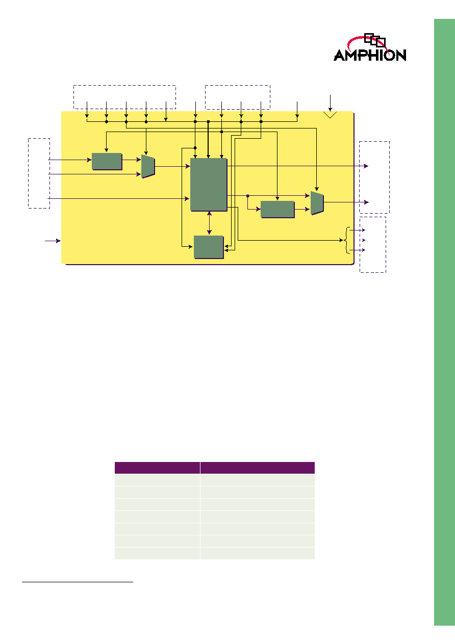
CS4100 FUNCTIONAL DESCRIPTION
AND OPERATION
The Amphion ADPCM core consists of 5 primary sections: an
ADPCM transcoding engine, logarithmic PCM/uniform PCM
expander, uniform PCM/logarithmic PCM compressor,
channel configuration and control, and coding states storage
memory, as illustrated in Figure 1. The core operates on one
input sample at a time, using 1, 6 or 16 clock cycles
1
to
complete the encoding or decoding. Multichannel coding is
implemented on time-multiplexing basis. The input/output
channel multiplexing and serial to/from parallel conversion
circuitry may be added to suit the target system as required.
The CS4100 cores have two channel addressing modes: the
flexible mode and the duplex mode
2
. In the duplex mode, half
of the channels are set to encode and half to decode. The
flexible mode allows each channel to be set, and reset,
individually. Within each of these modes the core can encode
data from three types of PCM format, as specified by ITU
standard G.711, to 2, 3, 4 or 5-bit ADPCM format. These are 8-
bit µ-law or A-law logarithmic PCM, 14-bit µ-law uniform
PCM or 13-bit A-law uniform PCM. The core can also decode
data from the 2, 3, 4 or 5-bit ADPCM format to the three types
of PCM format.
The cores are on-line configurable in terms of compression
rate and PCM law
3
and allow on-the-fly selection of PCM/
uniform PCM input/output. Each member of Amphion's
ADPCM family has been tested and verified to be fully
compliant using the ITU standard test vectors.
LOGARITHMIC
PCM/UNIFORM PCM EXPANDER
This block converts the input PCM signal from 8-bit A or µ-
law logarithmic PCM format to a 13-bit A-law or 14-bit µ-law
uniform PCM signal. This decoding is performed according to
the G.711 standard.
LOGARITHMIC
PCM/UNIFORM PCM COMPRESSOR
This block converts the output PCM signal from either 13-bit
A-law or 14-bit µ-law uniform PCM format to an 8-bit A- or µ-
law logarithmic PCM signal. This encoding is performed
according to the G.711 standard.
ADPCM TRANSCODING ENGINE
The primary encoding and decoding operations of the CS4100
ASVC take place within the ADPCM transcoding engine.
When encoding, the difference between the uniform PCM
input signal with a prediction of this signal is calculated. The
difference signal is then passed to an adaptive quantizer
where 5, 4, 3 or 2 binary digits are assigned as its value,
following the quantization methods stipulated by the G.726 or
G.727 standards. The result is the ADPCM signal for
transmission.
The current ADPCM signal is then used to predict the next
signal estimate. It is fed to an inverse adaptive quantizer and
the output is added to the current input signal estimate to
determine the reconstructed version of the input signal. This
signal and the output of the adaptive quantizer are then used
by the adaptive predictor to determine the estimate of the next
input signal, which is then fed back to determine the next
difference signal.
When decoding, the reverse procedure is performed. First, the
ADPCM signal is inversely quantized; then the resulting
signal is added to a prediction of this signal, forming a
reconstructed signal. The inversely quantized signal and the
reconstructed signal are used by the adaptive predictor to
determine the signal estimate for the next iteration.
This reconstructed signal is converted to a PCM signal before
passing through an additional block needed for synchronous
coding adjustment. This block prevents cumulative distortion
occurring on synchronous tandem codings. This is when the
signal is converted from PCM to ADPCM to PCM and back to
ADPCM. The idea is that when the PCM signal is converted
the resulting ADPCM signal is the same at every stage. The
output PCM signal from this block is the resulting decoded
output of the codec.
1.
16 clock cycles in the CS4110-30 cores, 1 clock cycle in the CS4180 and 6 clock cycles in the CS4190/91.
2.
The CS4180 operates in the flexible mode only.
3.
Compression rate and PCM law are selected on-the-fly in the CS4180.
3
TM
Figure 1: Input/Outputs for the Amphion ADPCM Cores
CODING STATES STORAGE MEMORY
The ADPCM algorithm requires from 279 to 283 bit states
1
for
each encoding or decoding channel (i.e., 558 to 566 bits per
duplex channel). These states are stored in the memory of the
ADPCM core.
To reduce the width of the data bus in the CS4110-30 and to
enable the core to complete an encoding or decoding
operation in 16 clock cycles, the memory is organized as 71
bits wide. This enables storage of a channel in 4 words, or 8
words for a duplex channel. In the CS4180 and CS4190/91, the
memory is organized as 279 or 282 bits wide (respectively) by
N words (where N is the number of channels), allowing
compete encoding or decoding operations in 1 (CS4180) or 6
(CS4190/91) clock cycles. Total memory requirements for the
members of the CS4100 family are found in Table 1.
In the CS4110-30 ASVCs, the core reads the coding states from
the memory in the first 4 clock cycles of the 16 clock cycle
operation period. In the last 4 clock cycles, the core writes the
update states back to the memory. In the CS4180, all memory
operations take place in 1 clock cycle; in the CS4190/91, these
memory read and write operations take 1 clock cycle each of
the 6 clock cycle operation period.
G726
Data
input
S
ID
Data
output
Status
outputs
I
SD
BSY**
ESI**
DSI**
EW
PCM
EDC
DSS
CHN
A-law/
-law
A-law/ -law
CFG
RST
CLR
MODE**
Uniform/
non-uniform
ADPCM
output signal
PCM
output signal
Logarithmic PCM
output signal
PCM output
Compressor
Memory
Mux
ADPCM
Engine
PCM input
Expander
Mux
Uniform PCM
output signal
Uniform/
non-uniform
Uniform PCM input
Logarithmic
PCM input
ADPCM input signal
*Scan Test Enable - only for the ASIC implementation
**Does not apply to CS4180
CLK
Coding control
Reset & Configuration
STE*
1.
The CS4110-30 use 283 bit states per channel, the CS4180 uses 279 and the CS4190 and 4191 use 282.
Table 1: Input/Output Descriptions
PRODUCT NUMBER
MEMORY REQUIREMENT
CS4110
4.544 Kbits
CS4120
18.176 Kbits
CS4125
36.352 Kbits
CS4130
72.704 Kbits
CS4180
209.250 Kbits
CS4190
288.768 Kbits
CS4191
577.536 Kbits

4
CS4100
ADPCM Speech Coders
CONFIGURATION AND CONTROL
The 8-bit wide CFG bus determines the compression rate and
law for each channel. The function of each bit is listed in Table
2. Note that the top 4 bits are only used in the duplex mode
and specify the law and compression rate for encoding; note
that these bits do not apply to the CS4180.
The input signal G726 is used to specify whether the G.726 or
G.727 is in use; when high the core operates per the G.726
standard, low indicates G.727.
Duplex (that is, the channels are split evenly between encode
and decode) and flexible channel addressing modes are
selected via the static MODE input. When MODE is high, the
core operates in duplex mode and when MODE is low the
core operates in the flexible mode. In the latter case, each
channel can operate as either an encoding or a decoding
channel.
Note that the CS4180 operates in the flexible mode only.
ENCODING/DECODING OPERATION
Encoding or decoding of one data sample is started by
asserting the data strobe signal (DSS). The input select signal
EDC defines whether the core performs an encoding or a
decoding operation. When EDC is HIGH, the core performs
encoding and the input S is taken. When EDC is LOW the core
will decode and the input ID is taken. Input signal PCM
specifies the type of encoding input data and decoding output
data, and input CHN specifies the channel the data belongs to,
as described in the previous sections.
The ADPCM core requires 1, 6 or 16 clock cycles (in the
CS4180, CS4190/91 and CS4110-30, respectively) to complete
an encoding or decoding operation for one data sample and
the output indicator BSY is de-asserted after the rising edge of
the 6th (or 16th) cycle (note: the output indicator BSY does not
apply to the CS4180, which completes all operations in a
single clock cycle). DSS can then be asserted after the rising
edge to start the next operation. The encoding and decoding
timing diagrams are depicted in Figure 3 and Figure 4,
respectively, for the CS4110-30 and Figures 5 and 6 for the
CS4190/91. The CS4180 completes all operations in a single
clock cycle.
Table 2: Codec Configuration Control Word
CFG BITS
DESCRIPTION
CONTROL CHOICE
Control Values
0
1
[7]
Selects either A-law or µ-law for encoding
in the duplex mode
µ-law
A-law
[6]
Controls whether even bit inversion/all bit inver-
sion is performed for A-law/µ-law encoding oper-
ations in the duplex mode
No bit inversion
Even bit inversion performed
for A-law
All bit inversion
performed for µ-law
Control Values
00
01
10
11
[5:4]
Controls the number of bits in the ADPCM
output word when encoding in the duplex mode
2 bits
3 bits
4 bits
5 bits
Control Values
0
1
[3]
Selects either A-law or µ-law for decoding
in the duplex mode or encoding/decoding
in the flexible mode
µ-law
A-law
[2]
Controls whether even bit inversion/all bit inver-
sion is performed for A-law/µ-law decoding oper-
ations in the duplex mode or encoding/decoding
in the flexible mode
No bit inversion
Even bit inversion performed
for A-law
All bit inversion
performed for µ-law
Control Values
00
01
10
11
[1:0]
Controls the number of bits in the ADPCM out-
put word when encoding in the duplex mode or
the number of bits in the ADPCM input word and
the ADPCM output word in the flexible mode.
2 bits
3 bits
4 bits
5 bits
5
TM
For the CS4110-30 and CS4190/91, it should be noted that:
∑
The core should be configured before an encoding or decoding
operation is started.
∑
When core busy indicator BSY is HIGH, asserting the control
signal DSS is ignored.
∑
Other input control signals, namely, EDC, CHN, PCM, G726 and
EW, are latched on the clock rising edge when DSS is HIGH and
BSY is LOW.
∑
Input data S and ID are also latched on the clock rising edge when
DSS is HIGH and BSY is LOW.
∑
The output data is registered.
∑
The encoding status indicator ESI indicates the internal encoding
state of the core. When it goes to LOW, the core has completed
the predictor state update. When it returns to HIGH, the encoding
output is available.
∑
The decoding status indicator (DSI) indicates the internal
decoding state of the core. When it goes to LOW, the core has
completed the predictor state update. When it returns to HIGH,
the decoding output is available.
∑
When an encoding or decoding operation is completed, signal
BSY returns to LOW and the core waits for DSS to be asserted to
start the next operation.
∑
Encoding and decoding can be performed in any order.
Output signals encode status indicator (ESI) and decode
status indicator (DSI) indicate the encoding and decoding
status, respectively. From the cycle when the codec picks up
the input data, ESI or DSI goes to `0'. In the cycle when the
encoding/decoding output is available, the corresponding
signal returns to `1'. Both the signals are set to `1' after reset
and before the first input.
CHANNEL SELECTION
The CHN input specifies the channel with which the input
data is associated when the core is performing a coding
operation or with which the CFG word is applied when the
core is performing channel reset and configuration. In the
flexible mode, one channel is either encoding or decoding and
the channel number is fully specified by CHN.
GLOBAL RESET AND CONFIGURATION
The asynchronous global reset signal, RST, resets all the
channels and configures them with the same compression rate
and PCM law; reset is activated when RST is asserted. RST
also resets all the registers in the core and interrupts the
encoding/decoding operation the core is performing. Global
configuration of the core is performed using the CFG input as
described earlier. The reset and configuration process starts on
the first rising clock edge after RST has been de-asserted and
continues for either 4*N cycles (CS4110-30) or N cycles
(CS4180-90), where N is the number of simplex channels
(where each duplex channel is considered as two simplex
channels). Reset occurs in 1 clock cycle for the CS4180.
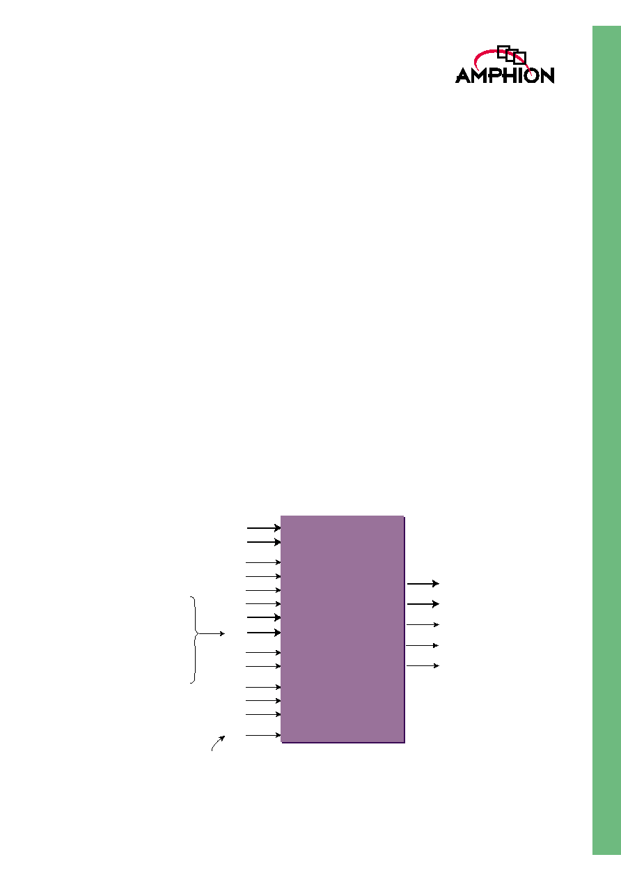
PIN/PORT DESCRIPTION
Table 3 describes the input and output ports (shown
graphically in Figure 2) of the CS4590 ADPCM codec. Unless
otherwise stated, all signals are active high and bit(0) is the
least significant bit.
Figure 2: ADPCM Core Pinouts
DSS
RST
CLR
CLK
STE
(Only for ASIC)
EDC
CHN
CFG[7:0]
EW[1:0]
PCM
MODE*
G726
ID[4:0]
S[13:0]
ESI*
DSI*
BSY*
SD[13:0]
I[4:0]
CS4100
ADPCM
CHN[3:0] for CS4110
CHN[5:0] for CS4120
CHN[6:0] for CS4125
CHN[7:0] for CS4130
CHN[9:0] for CS4180/CS4190
CHN[10:0] for CS4191
* Does not apply to CS4180

6
CS4100
ADPCM Speech Coders
Table 3: Input and Output Descriptions
Signal
I/O
Width
(Bits)
Description
Clk
I
1
Clock input, rising edge active
RST
I
1
Global reset and configuration symbol, active high, asynchronous to clock
CLR
I
Synchronous individual channel reset and configuration signal, active
high
MODE
(CS4110-30, CS4190/91)
I
1
Selects between the two modes of operation for the ADPCM core, the
duplex and flexible modes High: duplex mode Low: flexible mode
DSS
I
1
Input data strobe signal, active high, encoding/decoding is started
when asserted and BSY is low
EDC
I
1
Selects encode or decode operation:
High: encode
Low: decode
PCM
I
1
Logarithmic PCM or uniform PCM selection control signal
High: logarithmic PCM
Low: uniform PCM
S[13:0]
I
14
Logarithmic or uniform PCM input word for encoding
S[13:0]: µ-law uniform PCM input
S[13:1]: A-law uniform PCM input
S[7:0]: Logarithmic PCM input
ID
I
5
ADPCM input word for decoding
ID[4:3]: 2 bit ADPCM word, 16 Kbits/sec data rate
ID[4:2]: 3 bit ADPCM word, 24 Kbits/sec data rate
ID[4:1]: 4 bit ADPCM word, 32 Kbits/sec data rate
ID[4:0]: 5 bit ADPCM word, 40 Kbits/sec data rate
G726
I
1
Specifies G.726 or G.727 operation
High: G.726 standard
Low: G.727 standard
EW[1:0]
I
2
Specifies the number of G.727 enhancement bits
"00": 0 bits
"01": 1 bit
"10": 2 bits
"11": 3 bits
CHN[3-10:0]
I
4/6/7/8/
9/10/11
Specifies channel with which the input data is associated when the core is
performing coding operation or performing channel reset.
Width is 4 bits for CS4110, 6 bits for CS4120, 7 bits for CS4125 and 8 bits
for CS4130
Duplex mode: one channel encoding/decoding, channel number specified
by:
CHN[3:1] for the CS4110 core
CHN[5:1] for the CS4120 core
CHN[6:1] for the CS4125 core
CHN[7:1] for the CS4130 core
CHN[9:1] for the CS4180 and CS4190 cores
CHN[10:1] for the CS4191 core
(the LSB is ignored by the core)
In the flexible mode, one channel coding is either encoding or decoding
and the channel number is fully specified by CHN.

7
TM
* Does not apply to CS4180
CFG[7:0]
I
8
Channel configuration word defined as:
CFG(7): selects either A-law (CFG(7)=1), or µ-law (CFG(7)=0) for
encoding in the duplex mode
CFG(6): controls whether even bit inversion is performed for A-law
encoding operations. Even bit inversion on the 8-bit PCM input
data is performed when CFG(6) is `1'
CFG(5:4): controls the number of bits in the ADPCM output word when
encoding in the duplex mode
Encoding compress rates: 00 = 16 Kbit/s
01 = 24 Kbit/s
10 = 32 Kbit/s
11 = 40 Kbit/s
CFG(3): selects either A-law (CFG(3)=1), or µ-law (CFG(3)=0) for
decoding in the duplex mode or encoding/decoding in the flexi-
ble mode
CFG(2): controls whether even bit inversion is performed for A-law
decoding operations in the duplex mode or encoding/decoding
in the flexible mode. Even bit inversion on the 8-bit PCM input
data or the 8-bit PCM output data is performed when CFG(2) is
`1'
CFG(1:0): controls the number of bits in the ADPCM output word when
encoding in the duplex mode or the number of bits in the
ADPCM input word and the ADPCM output word in the flexible
mode
Decoding compress rates: 00 = 16 Kbit/s
01 = 24 Kbit/s
10 = 32 Kbit/s
11 = 40 Kbit/s
I[4:0]
O
5
ADPCM output word
I[4:3]: 2 bit ADPCM output, 16 Kbit/s
I[4:2]: 3 bit ADPCM output, 24 Kbit/s
I[4:1]: 4 bit ADPCM output, 32 Kbit/s
I[4:0]: 5 bit ADPCM output, 40 Kbit/s
SD[13:0]
O
14
Logarithmic or uniform PCM output word from decoding
SD[13:0]: µ-law uniform PCM output
SD[13:1]: A-law uniform PCM output
SD[7:0]: Logarithmic PCM output
BSY* (CS4110-30, CS4190)
O
1
Core busy indicator, active high, DSS is ignored when BSY is active
ESI* (CS4110-30, CS4190)
O
1
Encoding status indicator
DSI* (CS4110-30, CS4190)
O
1
Decoding status indicator
STE
I
1
Scan test enable (ASIC only)
During scan test the memory block must be bypassed to perform the test
During test, STE is set high, bypassing the memory. During normal opera-
tion of the core, STE is low
Table 3: Input and Output Descriptions
Signal
I/O
Width
(Bits)
Description

8
CS4100
ADPCM Speech Coders
Figure 3: Encoding Timing Characteristics of the CS4110-30
Figure 4: Decoding Timing Characteristics of the CS4110-30
CS4110-30 Timing
CLK
DSS
EDC
PCM
G726
EW
CHN
BSY
ESI
I
S
1
2
3
4
5
6
7
8
9
10
11
12
13
14
15
16
16 clock cycles
CLK
DSS
EDC
PCM
G726
EW
CHN
BSY
DSI
SD
ID
1
2
3
4
5
6
7
8
9
10
11
12
13
14
15 16
16 clock cycles

9
TM
Figure 5: Encoding Timing - CS4190/CS4191
Figure 6: Decoding Timing - CS4190/CS4191
CLK
DSS
EDC
PCM
G726
EW
CHN
BSY
ESI
I
S
6 clock
cycles
CS4190/CS4191 Timing
CLK
DSS
EDC
PCM
G726
EW
CHN
BSY
DSI
SD
ID
6 clock
cycles

10
CS4100
ADPCM Speech Coders
AVAILABILITY AND IMPLEMENTATION INFORMATION
ASIC CORES
For applications that require the high performance, low cost and high integration of an ASIC, Amphion delivers application
specific silicon cores that are pre-optimized to a targeted silicon technology by Amphion experts. Choose from off-the-shelf
versions of the CS4100 family available for many popular ASIC and foundry silicon supplier technologies or Amphion can port
the cores to a technology of your choice.
Consult your local Amphion representative for product specific performance information, current availability of individual
products, and lead times on ASIC core porting.
* Based on an SRAM density of 150 Kbits/mm
2
plus 20% area overhead peripheral circuitry
Table 4: CS4100 Family - ASIC Cores
PRODUCT
ID#
SILICON
VENDOR
PRODUCT
NAME/PROCESS
PERFORMANCE
LOGIC GATES
MEMORY AREA
(mm
2
)*
AVAILABILITY
CS4110TK
TSMC
180nm using Artisan
standard cell libraries
8 duplex channels at
2.048 MHz
19.6K
0.12
Now
CS4120TK
TSMC
180nm using Artisan
standard cell libraries
32 duplex channels at
8.192 MHz
19.8K
0.20
Now
CS4125TK
TSMC
180nm using Artisan
standard cell libraries
64 duplex channels at
16.384 MHz
19.8K
0.31
Now
CS4130TK
TSMC
180nm using Artisan
standard cell libraries
128 duplex channels
at 32.768 MHz
19.8K
0.52
Now
CS4190TK
TSMC
180nm using Artisan
standard cell libraries
512 duplex channels
at 49.152 MHz
26.7K
2.05
Now
CS4191TK
TSMC
180nm using Artisan
standard cell libraries
1024 duplex chan-
nels at 98.304 MHz
26.7K
4.1
Now

11
TM
PROGRAMMABLE LOGIC CORES
For ASIC prototyping or for projects requiring fast time-to-market of a programmable logic solution, Amphion programmable
logic cores offer the silicon-aware performance tuning found in all Amphion products, combined with the rapid design times
offered by today's leading programmable logic solutions.
*Not all the resources of every slice are used.
Table 5: CS4100 Family - Programmable Logic Cores
PRODUCT
ID#
SILICON
VENDOR
PROGRAMMABLE LOGIC
PRODUCT
PERFORMANCE
DEVICE RESOURCES
USED
AVAILABILITY
CS4110AA
Altera
Apex 20K FPGA
8 duplex channels at 2.048
MHz
4294 Logic Elements
11 ESB
Now
CS4110XV
Xilinx
Virtex FPGA
8 duplex channels at 2.048
MHz
1669 SLICEs
5 Block RAMs
Now
CS4120AA
Altera
Apex 20K FPGA
32 duplex channels at 8.192
MHz
4302 Logic Elements
16 ESB
Now
CS4120XV
Xilinx
Virtex FPGA
32 duplex channels at 8.192
MHz
1688 SLICEs
5 Block RAMs
Now
CS4125AA
Altera
Apex 20K FPGA
64 duplex channels at 16.384
MHz
4307 Logic Elements
24 ESB
Now
CS4125XV
Xilinx
Virtex FPGA
64 duplex channels at 16.384
MHz
1869 SLICEs
9 Block RAMs
Now
CS4180AA
Altera
Apex 20K FPGA
384 duplex channels at 6.144
MHz
6110 Logic Elements
149 ESB
Now
CS4180XE
Xilinx
Virtex-E FPGA
384 duplex channels at 6.144
MHz
2453 SLICEs*
70 Block RAMs
Now
CS4180X2
Xilinx
Virtex-II FPGA
512 duplex channels at 8.192
MHz
2439 SLICEs
16 Block RAMs 16s
Now

CS4100
ADPCM Speech Coders
s
TM
Virtual Components for the Converging World
CORPORATE HEADQUARTERS
Amphion Semiconductor Ltd
50 Malone Road
Belfast BT9 5BS
Northern Ireland, UK
Tel:
+44.28.9050.4000
Fax: +44.28.9050.4001
EUROPEAN SALES
Amphion Semiconductor Ltd
CBXII, West Wing
382-390 Midsummer Boulevard
Central Milton Keynes
MK9 2RG England, UK
Tel:
+44 1908 847109
Fax:
+44 1908 847580
WORLDWIDE SALES & MARKETING
Amphion Semiconductor, Inc
2001 Gateway Place, Suite 130W
San Jose, CA 95110
Tel:
(408) 441 1248
Fax: (408)
441
1239
CANADA & EAST COAST US SALES
Amphion Semiconductor, Inc
Montreal
Quebec
Canada
Tel:
(450) 455 5544
Fax: (450)
455
5543
Web: www.amphion.com
Email: info@amphion.com
© 2001-02 Amphion Semiconductor Ltd. All rights reserved.
Amphion, the Amphion logo,"Virtual Components for the Converging World", are trademarks of Amphion Semiconductor Ltd. All others are the property of their
respective owners.
12
05/02 Publication #: DS4100 v1.2
ABOUT AMPHION
Amphion (formerly Integrated
Silicon Systems) is the leading
supplier of speech coding, video/
image processing and channel
coding application specific silicon
cores for system-on-a-chip (SoC)
solutions in the broadband,
wireless, and mulitmedia markets.
SALES AGENTS
SPS-DA PTE LTD
21 Science Park Rd
#03-19 The Aquarius
Singapore Science P ark II
Singapore 117628
T el:
+65 774 9070
Fax:
+65 774 9071
SPINNAKER SYSTEMS INC
Hatchobori SF Bldg. 5F 3-12-8
Hatchobori, Chuo-ku
T oky o 104-0033 Japan
Tel:
+81 3 3551 2275
Fax:
+81 3 3351 2614
V oy ageur T echnical Sales Inc
1 Rue Holiday
T our Est, Suite 501
P oint Claire, Quebec
Canada H9R 5N3
T el:
(905) 672 0361
Fax:
(905) 677 4986
JASONTECH, INC
Hansang Building, Suite 300
Bangyidong 181-3, Songpaku
Seoul Korea 138-050
T el:
+82 2 420 6700
Fax:
+82 2 420 8600
Phoenix T echnologies Ltd
3 Gavish Street
Kfar -Saba, 44424
Israel
T el:
+972 9 7644 800
Fax:
+972 9 7644 801