 | –≠–ª–µ–∫—Ç—Ä–æ–Ω–Ω—ã–π –∫–æ–º–ø–æ–Ω–µ–Ω—Ç: CS4590TK | –°–∫–∞—á–∞—Ç—å:  PDF PDF  ZIP ZIP |

TM
Virtual Components for the Converging World
Amphion continues to expand its family of application-specific cores
1
See http://www.amphion.com for a current list of products
CS4590
High Channel Count ADPCM Speech Coder
Preliminary Datasheet
The CS4590 Adaptive Differential Pulse Code Modulator (ADPCM) core is designed to provide high
performance solutions for a broad range of applications requiring high channel count speech compression and
decompression. This high performance application specific silicon core performs the ITU G.726, G.726a, G.727
and G.727a ADPCM standards and has been tested and verified to be fully compliant using the ITU standard test
vectors. The CS4590 has been designed to support multichannel encoding/decoding on up to 3420 simplex
channels and has been handcrafted by Amphion to deliver high performance while minimizing power
consumption and silicon area for ASICs.
Figure 1: Example of CS4590 Integration in VON Application
Tone Detection
+
VAD
Channel
+
System Controller
ADPCM
CS4590
System
Memory
Packet
Processor
Packetized
Data
Packetized
Data
Voice/Fax
Voice/Fax
FEATURES
Fully compliant with ITU standards G.721,
G.723, G.726, G.726a, G.727 and G.727a
Supports large number of simultaneous
channels:
-
3420 in 130 nm technology
-
2340 in 180 nm technology
Uses external RAM for channel states
Online configurable for:
-
A-law or µ-law
-
Different compression rates
-
Uniform/logarithmic PCM
Burst mode as well as continuous operation
Operation on one input sample at a time
Low latency
-
8 clock cycles per channel coding
All synchronous, single clock design
Ease of integration
-
Simple core interface for easy integration into
larger systems.
KEY METRICS
1
Logic area:
39K gates
Maximum clock:
218MHz
APPLICATIONS
Wireless Communications
-
DECT phones
-
Digital cellular
Satellite Communications
Wired Telecommunications
-
Video conferencing
-
Voicemail systems
-
PBXs
1.
In 130nm technology. Please refer to Table 3 for information on 180nm technology.

2
CS4590
High Channel Count ADPCM Speech Coder
SPEECH COMPRESSION
In digital communications systems, speech coding
(compression and decompression) is used to reduce the bit
rate of a speech signal with no, or minimal, noticeable
degradation. Without such coding, the typical voice channel
would require 12-bit precision at a sampling rate of 8000 times
per second, equivalent to a data rate of 96 Kbits/second. As the
ear is less sensitive to errors at high volume levels than at low
volumes, logarithmic quantization can reduce this data rate to
64 Kbits/second with very little degradation; standard
techniques are the European A-law PCM and the American µ-
law PCM, both found in the CCITT G.711 standard. The data
rate can be further reduced through the use of ADPCM, which
transmits only the error between the actual signal and an
adaptively predicted signal. The current standards, G.726 and
G.727, support data rates of 40 Kbits/second down to as little
as 16 Kbits/second.
CS4590 FUNCTIONAL DESCRIPTION
The CS4590 core consists of an ADPCM Engine that performs
all the coding operation for the core. The core does not contain
internal memory, and all coding states are held externally. An
input coding state is fed into the core from an external input
register. The core performs coding on a specific channel for a
number of samples using this as the initial coding state. When
completed, the resulting state for that particular channel is
available on the output of the core for sending to the external
memory. Meanwhile, a coding state for the next channel is
retrieved from the external memory and is held in the input
register until it is required.
The CS4590 core consists of an ADPCM Transcoding Engine,
Logarithmic PCM/Uniform PCM Compander, Channel
Configuration and Control. The coding state storage memory
is external to the core, as illustrated in Figure 2.
ADPCM TRANSCODING ENGINE
The ADPCM engine performs the majority of the functionality
of the standards, the detail of which may be found in the ITU
G.726 and G.727 standards. The circuitry surrounding the
ADPCM engine controls the configuration of the codec,
performs the necessary conversion between different PCM
formats, and controls the input and output states. The
following section breaks down the components of the core
and details their functionality.
Figure 2: Block Diagram of the CS4590 ADPCM Core
G726
EW
PCM
EDC
DSS
EBI
IW
LAW
RST
INIT
START
Reset
Coding control
PCM input
Expander
Mux
ADPCM
Engine
PCM output
Compressor
Mux
Logarithmic PCM
output signal
PCM
output signal
Logarithmic
PCM Input
A-Law/
µ-Law
Uniform/
non-uniform
CLK
I
SD
Data
output
BSY
ESI
DSI
Status
output
ADPCM input signal
Uniform PCM input
A-Law/
µ-Law
ADPCM
output signal
Uniform PCM
output signal
Uniform/
non-uniform
278 bit Register
External State
Memory
S
ID
Data
Input
OSTATE / ISTATE
3
TM
LOGARITHMIC PCM/UNIFORM PCM
COMPANDER
Expansion to uniform PCM
The input PCM signal is converted from its 8-bit A- or
µ-law
logarithmic PCM format to a 13-bit A-law or 14-bit
µ-law
uniform PCM signal. The decoding is performed according to
the G.711 standard.
Compression to logarithmic PCM
The output PCM signal is converted from its 13-bit A-law or
14-bit
µ-law uniform PCM format to an 8-bit A or µ-law
logarithmic PCM format. The encoding is performed
according to the G.711 standard.
EXTERNAL MEMORY INTERFACE
The CS4590 codec has been developed specifically without
memory. The state memory is therefore supplied externally by
the user. The advantage of this is for applications in which the
codec will be operating on long durations on a particular
channel, i.e. it will be operating in a burst mode.
A size of memory required by the core is determined by the
number of simplex channels that the user applies the core to.
The ADPCM algorithm requires 278 bit states for each
encoding or decoding channel. In general a memory block of
Nx278 bits is needed by the core for the coding, where N is the
total number of simplex channels.
DATA FORMATS
The input to the ADPCM core for encoding is either 8-bit
logarithmic PCM, 14-bit
µ-law or 13-bit A-law uniform PCM
data. Before the input data can be encoded it must first be
expanded from the logarithmic PCM format to either the 13-
bit or 14-bit uniform PCM two's complement format,
depending on the coding law. This expansion is performed
according to the G.711 standard. The resulting encoded
output data is either a 2-, 3-, 4- or 5-bit ADPCM word,
depending on the data rate of the ADPCM signal, (16, 24, 32,
or 40 kbit/s respectively), as defined by the ITU G.726 and
G.727 standards. The input to the ADPCM core for decoding
is either a 2-, 3-, 4-, or 5-bit ADPCM data and the output is one
of the three PCM data formats.
Both the encode input port S and decode output port SD have
14 bits, of which the 8-bit PCM data occupies the lower 8 bits,
the A-law uniform PCM data the upper 13 bits, and the
µ-law
uniform all 14 bits, as illustrated in Figure 3.
On-the-fly selection of the logarithmic and uniform PCM data
is controlled by input signal PCM. When PCM is '1', the core
takes the 8-bit logarithmic PCM data as input for encoding
and output the 8-bit logarithmic PCM data for decoding.
When PCM is '0', the core takes the 14-bit or 13-bit uniform
PCM data, depending on the configuration, as input for
encoding and output the uniform PCM data for decoding.
The encode data output port I and decode data input port ID
have 5 bits each, for the 2, 3, 4 or 5 ADPCM word. The MSB is
the polarity and the 4 LSBs represent the magnitude. These
are also illustrated in Figure 3.
Figure 3: PCM and ADPCM Data Format
13
12
11
10
9
8
7
6
5
4
3
2
1
0
LSB
MSB
µ-law uniform PCM
A-law uniform PCM
8-bit logarithmic PCM
S, SD
4
3
2
1
0
LSB
MSB
I, ID
2-bit
ADPCM
3-bit ADPCM
5-bit ADPCM
4-bit ADPCM

4
CS4590
High Channel Count ADPCM Speech Coder
G.727 OR G.726 OPERATION
The ADPCM cores can perform either the G.727 or the G.726
standards. The input signal G726 is used to specify which
standard is being followed. If G726 is HIGH the G.726
standard is followed if, LOW, the core performs the G.727
standard
G.726A AND G.727A EXTENSIONS
The G.726a and G.727a recommendations are extensions that
specifically detail the interface of the G.726 and G.727 codecs
with 14-bit
µ-law uniform PCM. If 13-bit A-law uniform PCM
input is required then the value needs to be shifted a bit to the
left. Similarly, the uniform output result needs to be shifted
one bit right for the 13-bit A-law uniform PCM output
interface. If uniform PCM interfaces are required by the codec
the PCM conversion circuitry within the encoder and decoder
section are no longer needed.
PCM INPUT
The ADPCM cores can operate on uniform or logarithmic
PCM data. The choice of which is determined by the input
signal PCM. When PCM is LOW, uniform PCM operation is
selected, and when HIGH, logarithmic PCM is selected. With
logarithmic PCM, a further control (held within CFG) is then
used to select between A-law and µ-law PCM.
ENHANCEMENT BITS FOR G.727
OPERATION
One of the key differences between the two standards is that
the G.727 ADPCM encoded signal comprises of core bits and
enhancement bits. Signal EW is a two-bit binary number,
which specifies the number of enhancement bits when the
codec works in G.727 coding mode. It is also asserted at the
same time when DSS is asserted. If its value is out of the valid
range (core bits + enhancement bits
5), the maximal allowed
is assumed.
EBI
When HIGH even bit inversion is performed for A-law or all
bit inversion performed for
µ-law.
IW
Controls the number of bits in the ADPCM input word when
decoding or the number of bits in the ADPCM output word
when encoding. The settings for the number of bits in the
ADPCM word, i.e., the compression rate, are detailed in
Table 1.
LAW
Controls the format of the PCM data. If HIGH, A-law
compression is used, if LOW,
µ-law is used.
RESET
The asynchronous global reset signal, RST, resets all registers
within the core.
Table 1: Compression Rate Settings
IW
G.726 Standard
G.727 Standard
Core bits
bit 1
bit 0
ADPCM Word Length
ADPCM Data Rate (kbit/s)
0
0
2
16
2
0
1
3
24
3
1
0
4
32
4
1
1
5
40
Not valid
5
TM
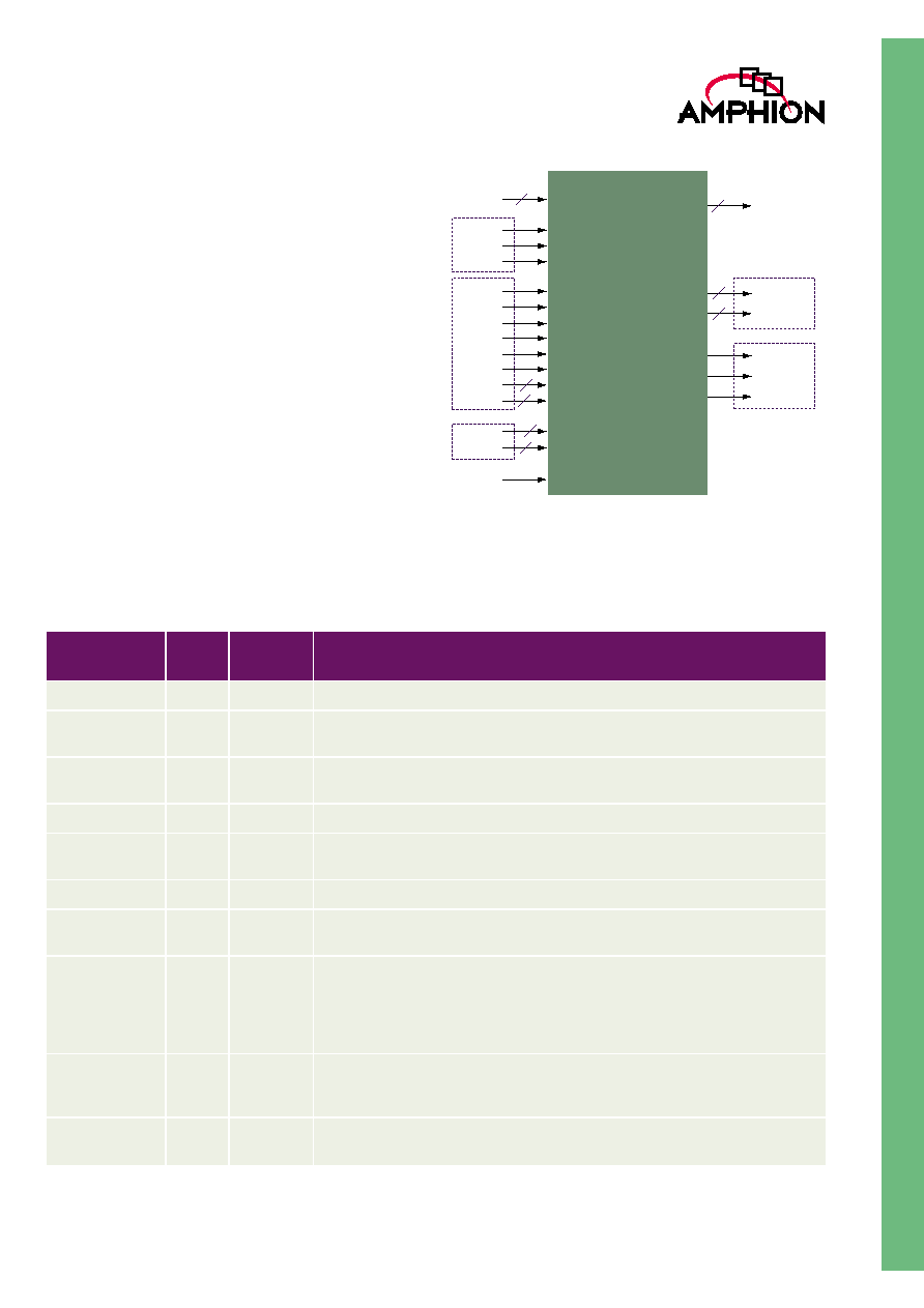
CS4590 SYMBOL AND PIN
DESCRIPTION
Table 2 describes the input and output ports (shown
graphically in Figure 4) of the CS4590 ADPCM codec. Unless
otherwise stated, all signals are active high and bit(0) is the
least significant bit.
Figure 4: CS4590 Symbol
ISTATE
START
INIT
RST
DSS
LAW
EDC
PCM
G726
EBI
IW
EW
S
ID
CLK
ADPCM
CS4590
Core
OSTATE
Data
Output
Status
Outputs
I
SD
BSY
ESI
DSI
278
5
14
278
2
2
14
5
Table 2: Input/Output Descriptions
Signal
I/O
Width
(Bits)
Description
ISTATE
I
278
Channel state held in memory for a particular channel
START
I
1
Signifies when coding is switching to a different channel. When HIGH and INIT
is LOW, channel is configured and input ISTATE is used to begin coding.
INIT
I
1
Initialization - when HIGH and START HIGH input state set to ITU initial values
and channel is configured.
RST
I
1
Global reset.
DSS
I
1
Input data strobe signal: encoding/decoding started when DSS is HIGH and
BSY is LOW
LAW
I
1
A-law if HIGH, µ-law if LOW
EDC
I
1
HIGH - encoding, input S is taken
LOW - decoding, input ID is taken.
PCM
I
1
The ADPCM cores can operate on uniform or logarithmic PCM data. The choice
of which is determined by input signal PCM. When PCM = 1, Logarithmic PCM
operation is selected, and when 0, uniform PCM is selected. With logarithmic
PCM, a further control signal (LAW) is then used to select between A-law and
µ-
law PCM.
G726
I
1
Standard control input:
HIGH - G.726 standard
LOW - G.727 standard
EBI
I
1
If HIGH even bit inversion for A-law, all bit inversion for
µ
-law
If LOW no even bit inversion

6
CS4590
High Channel Count ADPCM Speech Coder
IW
I
2
ADPCM output compression rate when decoding:
G.726:
00=16kbit/s
01=24kbit/s
10=32kbit/s
11=40kbit/s.
G.727:
00=2 core bits
01=3 core bits
10=4 core bits
11 not allowed
EW
I
2
Specifies the number of enhancement bits used when the codec works in G.727
coding mode. It is also asserted at the same time when the DSS is asserted. If
its value is out of the valid (core bits + enhancement bits
5), the maximal
allowed is assumed:
00
no enhancement bits
01
1 enhancement bit
01
2 enhancement bits
01
3 enhancement bits
S
I
14
PCM input word for encoding
ID
I
5
ADPCM input word for decoding:
ID(4) : bit no.1 the polarity
ID(4:3): 2 bit ADPCM -16 kbit/s
ID(4:2): 3 bit ADPCM - 24 kbit/s
ID(4:1): 4 bit ADPCM - 32 kbit/s
ID(4:0): 5 bit ADPCM - 40 kbit/s
CLK
I
The core uses a single clock to operate. All registers in the core operate on the
rising edge of the input clock CLK. Data inputs are latched on the clock rising
edge and outputs are generated on the clock rising edge
OSTATE
O
278
Channel state fed out to memory for a particular channel.
I
O
5
I(4) : bit no.1 the polarity
I(4:3): 2 bit ADPCM - 16kbits/s
I(4:2): 3 bit ADPCM - 24 kbits/s
I(4:1): 4 bit ADPCM - 32 kbits/s
I(4:0): 5 bit ADPCM - 40 kbits/s
SD
O
14
PCM output word from decoding.
BSY
O
1
Core busy indicator, active HIGH, DSS ignored when active.
ESI
O
1
Encoding status indicator.
DSI
O
1
Decoding status indicator.
Table 2: Input/Output Descriptions
Signal
I/O
Width
(Bits)
Description

7
TM
OPERATION OF THE CS4590
The CS4590 core operates on a particular channel on bursts of
samples at a time. The START input signal signifies the start of
coding operations for a particular channel. When START is
HIGH the core reads in the values held in the input port
ISTATE into the core, and reads in all the configuration data
for that channel and sets the channel configuration.
INIT is an initialization control input signal. When HIGH it
signifies that the output states held in the output register of
the ADPCM core are ignored and not fed to external state
memory. In addition it specifies that the internal states of the
core are set to ITU initial values. Therefore if START is HIGH
when INIT is HIGH then the initial values for ISTATE are used
to begin the coding.
Please note that the signal CFG within the diagrams refers to
all the input channel configuration controls the (EDC, PCM,
LAW, IW, EW, G726 and EBI), collected together. They are
instantiated within the core as individual ports but have been
collected together within the diagram for clarity.
The timing diagrams show an example implementation with 3
channels A, B and C, and each operates on a burst of 5
samples. Figure 3 shows the initialisation and coding
operations for Channel A.
The data strobe signal DSS, when HIGH, signifies the start of a
new coding operation. Each coding operation (whether being
encoding or decoding) requires 8 clock cycles after which DSS
may be set HIGH to bring in the next sample for coding. This
may be repeated until all the samples within the BURST are
completed for that channel. When DSS is HIGH, the input
select signal EDC is read. This signal defines whether the core
performs an encoding or decoding operation. When EDC is
HIGH, the core performs encoding and the input S is taken.
When EDC is LOW the core will decode, and the input ID is
taken. Input signal PCM specifies the type of encoding input
data and decoding output data. The output signals ESI
(encode status indicator) and DSI (decode status indicator)
indicate the encoding and decoding status respectively. From
the cycle when the codec picks up the input data, ESI or DSI
goes to '0'. In the cycle when the encoding/decoding output is
available, the corresponding signal returns to '1'. Both the
signals are set to '1' after reset and before the first input.
It should be noted that these timing diagrams provide only
the functional timing for the operation, since the actual timing
depends on the target implementation technology.

8
CS4590
High Channel Count ADPCM Speech Coder
TIMING DIAGRAMS
Figure 5 shows the timing diagrams for an example set up where 3 channels operate in bursts of 5 samples at a time. An example
organization of the coding operations for each of the 3 channels is summarized in Table 3.
Table 3: Organization of the Coding Operations for Different Channels of the CS4590
Clock Cycle
1-8
9-16
17-24
25-32
33-40
Channel
Channel A
Coding operation for channel
1
2
3
4
5
INIT HIGH at cycle
1
START HIGH at cycle
1
DSS HIGH at cycle
1
9
17
25
33
Clock Cycle
41-48
49-56
57-64
65-72
73-80
Channel
Channel B
Coding operation for channel
1
2
3
4
5
INIT HIGH at cycle
41
START HIGH at cycle
41
DSS HIGH at cycle
41
49
57
65
73
Clock Cycle
81-88
89-96
97-104
105-112
113-120
Channel
Channel C
Coding operation for channel
1
2
3
4
5
INIT HIGH at cycle
1
START HIGH at cycle
1
DSS HIGH at cycle
81
89
97
105
113
Clock Cycle
121-128
129-136
137-144
145-152
153-160
Channel
Channel A
Coding operation for channel
6
7
8
9
10
START HIGH at cycle
121
DSS HIGH at cycle
121
129
137
145
153
9
TM
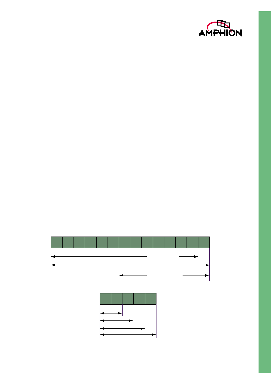
Figure 5: Sample Timing Diagram (3 channels operating in bursts of 5 samples at a time)
1
2
3
4
5
6
7
8
9
10
11
12
13
15
16
17
18
19
20
21
22
23
24
25
26
27
28
29
14
CLK
INIT
INIT is an initialization control signal. When HIGH, it signifies that the output states held in the register of the ADPCM core are ignored and not fed to external state memory. In addition,
it specifies that the internal states of the core are set to ITU initial values.
START
The START input signal signifies the start of coding operations for a particular channel. When START is HIGH the core reads in the values held in the input port ISTATE into the core and
reads in all the configuration data for that channel configuration. The cycle after START the output state from the previous channel valid on the output port OSTATE.
All the channel configuration control - EDC, LAW, EBI, EW, IW, PCM, G716 - read when START HIGH
CFG
DSS
DSS, when HIGH, signifies the start of a new coding operation. Each coding operation (whether encoding or decoding) requires 8 clock cycles after which DSS may be set HIGH to
bring in the next sample for coding. This may be repeated until all the samples within the BURST are completed for the channel.
Input state ISTATE for current channel - ignored if INIT is HIGH
ISTATE
OSTATE
ISTATE if INIT LOW / ITU initial state if INIT HIGH
STATE 1
STATE 2
STATE 3
S or SD
input data
Inputs read in when DSS HIGH
ESI or DSI
In4
In3
In1
In2
Data input 1 for
channel A
Data input 2 for
channel A
Data input 4 for
channel A
Data input 3 for
channel A
Out1
Out2
Out3
Encoded output I valid when ESI is HIGH and decoded output SD is valid when DSI is HIGH
SD or I
output data
BSY
Data output 1 for channel A
Data output 2 for channel A
Data output 3 for channel A
8 clock cycles
8 clock cycles
8 clock cycles
Coding 1 for channel A
Coding 2 for channel A
Coding 3 for channel A

10
CS4590
High Channel Count ADPCM Speech Coder
AVAILABILITY AND IMPLEMENTATION INFORMATION
ASIC CORES
For applications that require the high performance, low cost and high integration of an ASIC, Amphion delivers application
specific silicon cores that are pre-optimized to a targeted silicon technology by Amphion experts.
Consult your local Amphion representative for product specific performance information, current availability of individual
products, and lead times on ASIC core porting.
Table 4: CS4590 ASIC Cores
PRODUCT
ID#
SILICON
VENDOR
PROCESS
TECHNOLOGY
# of CHANNELS
CLOCK SPEED
(MHz)
LOGIC GATES
AVAILABILITY
CS4590TK
TSMC
130 nm
3420
218
39K
Now
CS4590TK
TSMC
180 nm
2340
150
35K
Now

CS4590
High Channel Count ADPCM Speech Coder
TM
Virtual Components for the Converging World
CORPORATE HEADQUARTERS
Amphion Semiconductor Ltd
50 Malone Road
Belfast BT9 5BS
Northern Ireland, UK
Tel:
+44.28.9050.4000
Fax: +44.28.9050.4001
EUROPEAN SALES
Amphion Semiconductor Ltd
CBXII, West Wing
382-390 Midsummer Boulevard
Central Milton Keynes
MK9 2RG England, UK
Tel:
+44 1908 847109
Fax:
+44 1908 847580
WORLDWIDE SALES & MARKETING
Amphion Semiconductor, Inc
2001 Gateway Place, Suite 130W
San Jose, CA 95110
Tel:
(408) 441 1248
Fax: (408)
441
1239
CANADA & EAST COAST US SALES
Amphion Semiconductor, Inc
Montreal
Quebec
Canada
Tel:
(450) 455 5544
Fax: (450)
455
5543
Web: www.amphion.com
Email: info@amphion.com
© 2002 Amphion Semiconductor Ltd. All rights reserved.
Amphion, the Amphion logo,"Virtual Components for the Converging World", are trademarks of Amphion Semiconductor Ltd. All others are the property of their
respective owners.
11
05/02 Publication #: DS4590 v1.2
ABOUT AMPHION
Amphion (formerly Integrated
Silicon Systems) is the leading
supplier of speech coding, video/
image processing and channel
coding application specific silicon
cores for system-on-a-chip (SoC)
solutions in the broadband,
wireless, and mulitmedia markets.
SALES AGENTS
SPS-DA PTE LTD
21 Science Park Rd
#03-19 The Aquarius
Singapore Science P ark II
Singapore 117628
T el:
+65 774 9070
Fax:
+65 774 9071
SPINNAKER SYSTEMS INC
Hatchobori SF Bldg. 5F 3-12-8
Hatchobori, Chuo-ku
T oky o 104-0033 Japan
Tel:
+81 3 3551 2275
Fax:
+81 3 3351 2614
V oy ageur T echnical Sales Inc
1 Rue Holiday
T our Est, Suite 501
P oint Claire, Quebec
Canada H9R 5N3
T el:
(905) 672 0361
Fax:
(905) 677 4986
JASONTECH, INC
Hansang Building, Suite 300
Bangyidong 181-3, Songpaku
Seoul Korea 138-050
T el:
+82 2 420 6700
Fax:
+82 2 420 8600
Phoenix T echnologies Ltd
3 Gavish Street
Kfar -Saba, 44424
Israel
T el:
+972 9 7644 800
Fax:
+972 9 7644 801