 | –≠–ª–µ–∫—Ç—Ä–æ–Ω–Ω—ã–π –∫–æ–º–ø–æ–Ω–µ–Ω—Ç: CS6150AC | –°–∫–∞—á–∞—Ç—å:  PDF PDF  ZIP ZIP |
TM
Virtual Components for the Converging World
Amphion continues to expand its family of application-specific cores
1
See http://www.amphion.com for a current list of products
CS6150
Motion JPEG Decoder
The CS6150 Motion JPEG (M-JPEG) Decoder is a highly integrated virtual component solution for leading-edge
image decompression applications. Its high performance is capable of sustaining data rates of over 185 mega-
samples/sec ≠ delivering full motion, full color video images up to 4 megapixels
1
. Fully compliant with the
baseline JPEG standard, the CS6150 delivers the optimal performance and low cost that only an application
specific core can provide, making it the ideal solution for video conferencing and office automation equipment.
When used in conjunction with the companion CS6100 JPEG encoder, the CS6150 provides the heart of a high
performance video storage or broadcast system. The CS6150 is available in both ASIC and programmable logic
versions that have been handcrafted by Amphion to deliver high performance with low-power and minimal
silicon area.
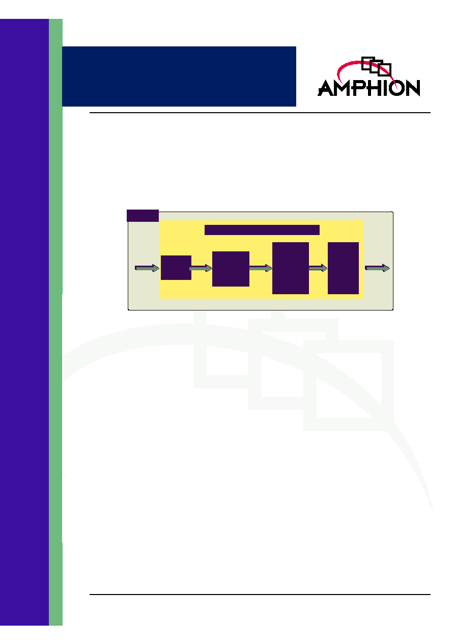
Figure 1: CS6150 Overview Diagram
Inverse
Frequency
Transform
(iDCT)
Inverse
Quantization
Configuration & Control Interface
C S 6 1 5 0
Run Length
& Variable
Length
Decoder
JPEG
Stream
Parser
Image
Data
JPEG
Stream
Input
FEATURES
High Performance
-
Sustained 185 Msamples/second decoding
capability
-
Single sample per clock cycle processing
Low Power
-
Zero standby power
-
Fully synchronous operation
Fully Compliant with Baseline JPEG Standard
ISO/IEC 10918≠1/2
-
Supports interleaved and non-interleaved
scans
-
Supports image sizes to 64k by 64k
-
Support for 4 user-defined Huffman tables
and 4 programmable quantization tables
Autonomous Operation
-
Simple FIFO-like interface for JPEG decoding
stream input
-
No microprocessor control or pre-processing
required
-
Decodes quantization and Huffman tables
and parameter information from JPEG bit-
stream
Ease of Integration
-
Targeted netlist
-
Simple core interface for easy integration into
larger systems
KEY METRICS
Logic:
60k gates
Memory:
9.6 kbits RAM
Maximum Frequency:
185 MHz
APPLICATIONS
Interactive Video
-
Full duplex, high performance video confer-
encing when used with companion CS6100
JPEG encoder
High performance, low cost document pro-
cessing
-
Photo printers
-
Digital copiers
-
Multifunction printers
Remote Video
-
Surveillance systems
1
30 frame/sec, 24-bit color images with three components in 4:2:0 format

2
CS6150
Motion JPEG Decoder
CS6150 FUNCTIONAL DESCRIPTION
The CS6150 core is a highly integrated JPEG decoder suitable for a wide range of imaging applications. Designed for continuous
data flow ≠ one image sample per clock cycle ≠ the CS6150 can address the most demanding frame-based video decompression
applications. In addition, fully synchronous operation and zero-power standby make it ideal for low power applications. The
highly autonomous design extracts all relevant information (quantization and Huffman tables and parameter information) from
the JPEG bitstream and requires no software overhead. The CS6150 is a powerful and flexible JPEG decoding solution.
PARSER
This unit parses and checks the JPEG input stream,
automatically detecting and processing all the JPEG marker
segments without the need for a processor and signalling any
detected errors. If an error is found the parser stops reading
the JPEG stream and waits to be reset. After identifying the
segments, it re-directs the data to the appropriate units in the
decoder to be stored or processed. In addition, the JPEG file
header information and marker segments can be output on
the masked JPEG output port (DecJpg) in accordance with the
value set on the JPEG mask control port.
VARIABLE LENGTH DECODER
The variable length decoding unit (VLD) consists of both the
Huffman decoder (HUFF) and run length decoding unit
(RLD). Huffman decoding techniques are first applied to the
stream of parsed data to regenerate the Run-Size data pairs.
The decoder detects the uniquely identifiable Huffman codes
and converts them to corresponding Run-Size pairs read from
a look-up table stored in the Huffman Table memory
(HTMem). The CS6150 can store four user-defined Huffman
tables, two for DC coefficients and two for AC coefficients, the
DC and AC coefficients being Huffman decoded separately.
The Run-Size data pairs output from the Huffman decoder are
then buffered in the Run-Length Memory (RLMem) and
loaded into the run length decoder unit. The RLD
decompresses the data stream by converting the Run-Size
data pairs into 8x8 blocks of quantized DCT coefficient data.
The decompression produced by the VLD is data dependent
and thus latency can vary.
COEFFICIENT DEQUANTIZATION
The coefficient dequantization (DQT) unit multiplies each of
the 64 DCT coefficients in an image block by the values
specified in one of the four quantization tables. The purpose
of the dequantization process is to rescale the DCT coeffi-
cients and restore their original magnitude. Up to four user
programmable quantization tables can be stored in the
quantization table memory (QTMem). The 11-bit DCT data is
loaded into DQT directly from the VLD. The DQT unit
quantizes one sample per clock cycle with a latency between
the first sample in and first sample out of 2 clock cycles. The
11-bit dequantized DCT coefficients are then output from the
DQT unit for direct input to the inverse frequency transform.
INVERSE FREQUENCY TRANSFORM
The inverse frequency transform (IFT) unit accepts 64-byte
(8 x 8) blocks of frequency coefficients and converts these to
8 x 8 blocks of image sample data in raster format using a 2D
inverse discrete cosine transform (IDCT) architecture. This is
implemented as two, 1-D IDCT operations, with the
intermediate results being stored in the dual-port transpose
memory (TRMem) buffer. The architecture of the IFT unit
allows for continuous one sample per cycle operation with a
latency between first sample in and first coefficient out of 83
clock cycles. The 8-bit decoded image sample data is streamed
out from the IFT unit via the output pixel interface of the core.
CONTROLLER
The controller unit consists of a code control state machine
(DecCtrl) that manages the operation of the CS6150. It is used
to build the control parameters for decoding from the input
JPEG stream and for detecting illegal and corrupted markers
within the stream.
3
TM
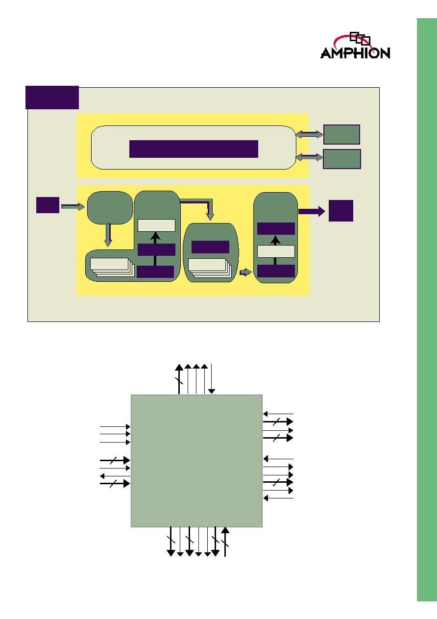
CS6150 DIAGRAM
Figure 2: CS6150 JPEG Decoder Block Diagram
CS6150 SYMBOL & PIN DESCRIPTION
Figure 3: CS6150 Symbol
Image
Data
JPEG
Stream
Variable Length
Decoder
(RLD) & (HUFF)
ZZMem
Huffman
Decoder
HTMem
JPEG
Data Stream
Parser
(JSP)
C S 6 1 5 0
Coefficient
Dequantization (DT)
QTMem
Multiplier
Code Control
Parameter
Extraction
Test
Access Port
Inverse
Frequency
Transform
(IFT)
iDCT
iDCT
TRMem
Run Length
Decoder
DecJpgNext
DecJpg[7:0]
DecJpgAvail
DecSoiEoi[1:0]
TType
TSOS
TSOB
TData[10:0]
TValid
TestEn
CLK
RSTn
CLR
JpgIn[7:0]
JpgInStrb
JpgInRdy
JpgMask[4:0]
PT
ype[3:0]
PV
alue[15:0]
PV
alid
SigSoS
DecFlags[7:0]
InitProg
TblDef[7:0]
PixOutEnab
PixOutLast
PixOutV
alid
PixOutSob
PixOut[7:0]

4
CS6150
Motion JPEG Decoder
Table 1: I/O Signal Description
SIGNAL
PORT
WIDTH
(BITS)
I/O
DESCRIPTION
GLOBAL SIGNALS
CLK
1
Input
Clock
Clock - rising edge active
RSTn
1
Input
Reset
Asynchronous reset (power-on reset)
CLR
1
Input
Clear
Synchronous reset
JPEG INPUT PORT
JpgIn
8
Input
JPEG Input
JPEG data input port
JpgInStrb
1
Input
JPEG Input Strobe
JPEG data input strobe
JpgInRdy
1
Output
JPEG INPUT Ready
Indicates that the CS6150 is ready to accept JPEG input data
DECODING MASKED JPEG OUTPUT PORT
JpgMask
5
Input
JPEG Mask
DecJpg output configuration port
DecJpgNext
1
Input
Decoded JPEG Next
Informs core to place next 8-bit word of masked JPEG output data onto DecJpg.
The data is held if DecJpgNext is not asserted.
DecJpg
8
Output
Decoded JPEG
Masked output JPEG data
DecJpgAvail
1
Output
Decoded JPEG Available
Indicates that valid data is available on DecJpg
DecSoiEoi
2
Output
Decoded Start of Image and End of Image
Indicates the start and end of image
PIXEL OUT PORT
PixOut
8
Output
Pixel Output
Pixel output data
PixOutSob
1
Output
Pixel Output Start of Block
Marks the first value in each 8x8-output block of pixel data
PixOutValid
1
Output
Pixel Output Valid
Indicates valid pixel output data
PixOutLast
1
Output
Pixel Output Last
Indicates the last block of decoded pixel data of a scan
PixOutEnab
1
Input
Pixel Output Enable
Informs core to output 8x8 blocks of pixel data onto PixOut
TEST PORT
TType
1
Input
Test Type
Test type selector
TSOS
1
Output
Test Start of Scan
Marks the first value in the first 8x8-output block of test data
TSOB
1
Output
Test Start of Block
Marks the first value in each 8x8-output block of test data
TData
11
Output
Test Data
11-bit output test data port ≠ displays DCT coefficients or quantized coefficients
TValid
1
Output
Test Data Valid
Indicates valid test data output
TestEn
1
Input
Test Enable
Causes memories to be bypassed for test purposes
5
TM
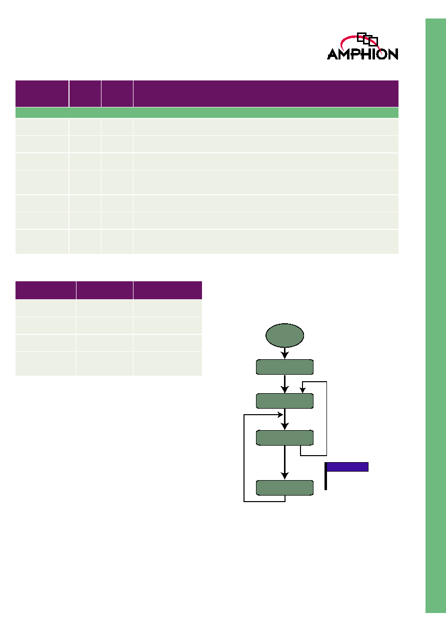
STATE DESCRIPTIONS
The major operating modes and states of the CS6150 are
shown in Figure 4.
INITIALIZATION
Following the assertion of the reset signal (RSTn) the core
enters the Initialization state for 384 clock cycles. During this
period the internal memories are initialized. After exiting the
Initialization state the core enters the Idle state.
IDLE STATE
The core enters the Idle state after exiting Initialization state or
after the assertion of CLR. It also enters Idle state after
processing an EOI whilst in the Marker Decode state.
The core remains in the Idle state until being presented with
the first byte of a JPEG stream on port JpgIn. If the core exits
Idle state due to an input on port JpgIn it enters either Marker
Decode state.
Figure 4: CS6150 Decoder States
STATUS & CONTROL
PType
4
Input
Parameter Type
Signal specifying parameters to be placed on port PValue
PValue
16
Output
Parameter Value
Decoding parameter bus
PValid
1
Output
Parameter Valid
Indicates valid coding parameters
SigSOS
1
Output
Signal Start of Scan
Indicates that an SOS segment has been input via JpgIn input and the decoder is about to start
decoding a scan
DecFlags
8
Output
Decoder Flags
CS6150 internal status and error flag status register
InitProg
1
Output
Initialization In Progress
Indicates that the CS6150 is currently initializing its initial memories
TblDef
8
Output
Tables Defined
Indicates number of tables defined. Bits[7:4] indicate Huffman tables. Bits[3:0] indicate quantiza-
tion tables, 1bit/table
Table 1: I/O Signal Description
SIGNAL
PORT
WIDTH
(BITS)
I/O
DESCRIPTION
Table 2: Memory BLock Size Information
MEMORY BLOCK CONFIGURATION
(WORDSxBITS)
PORTS
Huffman Tables
(HTMem)
384 x 8
Single Port, synchronous
Transpose Memory
(TRMem)
64 x 15
Dual Port, synchronous
Quantization Tables
(QTMem)
512 x 8
Single Port, synchronous
Run-Length
Decoder Memory
(RLMem)
64 x 22
Dual Port, synchronous
Reset
Initialization
Idle
Entropy Decode
Marker Decode
1 SOS Input
2 EOI Input
KEY
1
2
6
CS6150
Motion JPEG Decoder
DECODER OPERATION
MARKER DECODE STATE
The core enters the Marker Decode state when it receives the
first byte of the decode stream and remains there until it
decodes either an SOS or EOI marker. If it decodes an SOS
marker and has already received all the other information
needed to decode the scan, such as the Huffman tables, it
enters Entropy Decode state, otherwise it will assert an error
flag on the CodFlags output port and will stop accepting data.
If it receives an EOI it enters Idle state. The JpgInProg output
[CodFlags(0)] is asserted when the core starts to process input
JpgIn and is de-asserted when the EOI marker has been
loaded into the core on the JpgIn input. If the core enters
Marker Decode state from Idle state it expects to receive an
SOI as the first input and will discard all input until an SOI is
received. When recovering from an error in the decode
stream, this allows the core to discard the end of corrupt
stream and to locate the start of the new stream. This
synchronization feature could be useful if the decode stream
is arriving from a noisy channel in an MJPEG system and
means that the system does not have to locate the start of the
stream for the core.
When in Marker Decode state the core automatically detects
the JPEG marker segments listed in Table 3.
After detecting a segment the core decodes and stores the
information in the segment and checks that the information is
valid. If the information contains an error, then the core will
assert an error flag on the DecFlags output port and will stop
accepting data. The error can be cleared by asserting RSTn or
CLR.
As the segments are being decoded from the decode-stream
they can also be output by the core on port DecJpg, and the
user can select the ones that are actually output by setting bits
on the JPEG Mask port according to Table 6. This could be
used, for example, as a simple method for the user to gain
access to the information contained in the APP markers
without having to parse the data stream.
ENTROPY DECODE STATE
The core enters Entropy Decode state after decoding an SOS
from the decode stream. In Entropy Decode state it decodes
the pixel data from the entropy-coded segments,
automatically selecting the correct Huffman and quantization
tables to use for each component. If an error is detected in the
entropy coded data the core will assert DecHfError
(DecFlags[7]), and will attempt to recover by discarding
entropy coded data up to the next Restart Marker or the end
of the image, whilst still producing the expected amount of
pixel data. The DecHfError signal is cleared by RSTn or CLR
and by the start of a new decode-stream and, as a result, the
core does not need the user to respond to the DecHfError
signal. The DecInProg signal will be asserted whilst decoding
a scan.
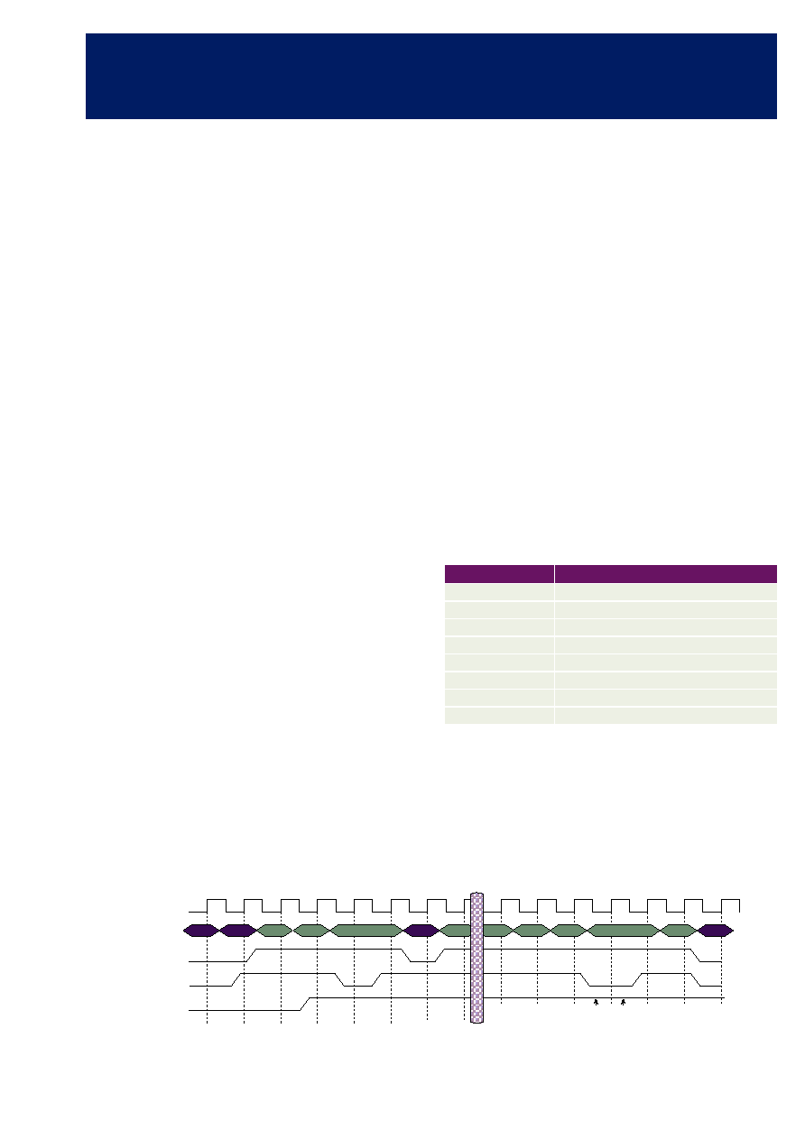
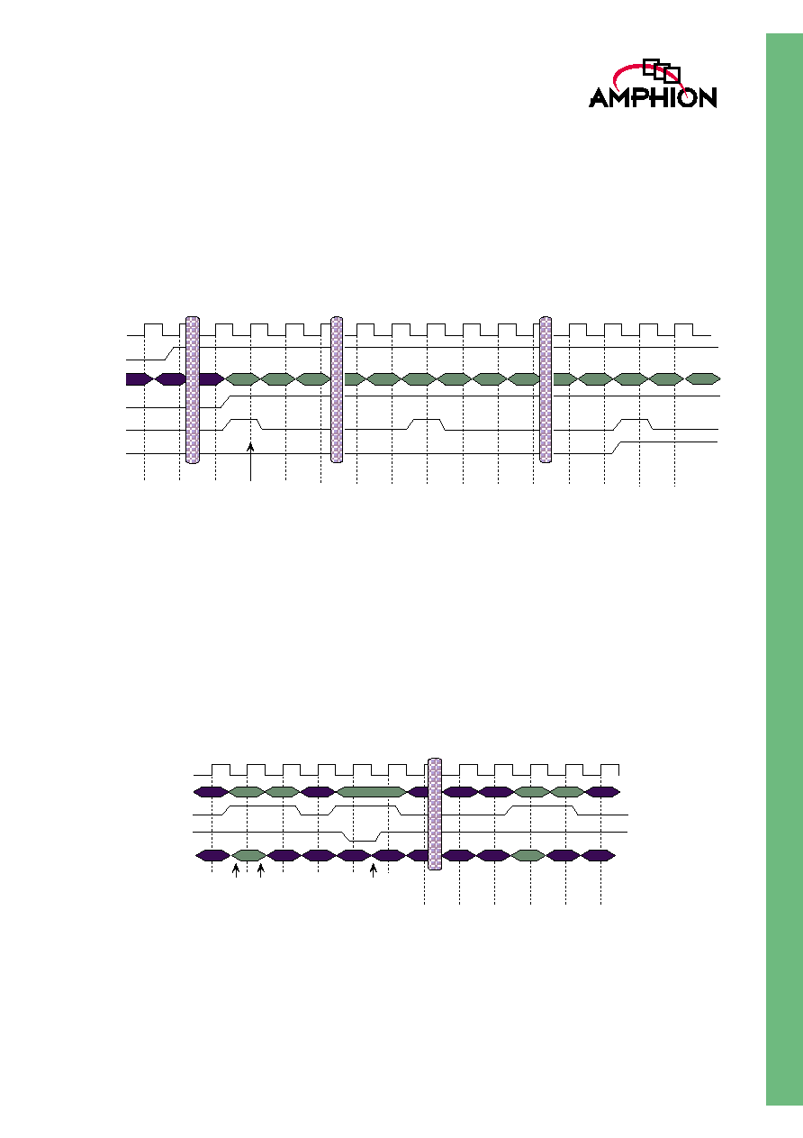
JPEG DATA STREAM INPUT PORT
Loading of the compressed JPEG input image data is
performed using the JpgIn interface. The data stream is input
to CS6150 via the JpgIn[7:0] port. This stream must also be
accompanied by a data valid signal, JpgInStrb, which must be
asserted coincident with all valid samples. The data interface
operates synchronously, reading a compressed JPEG data
sample at the rising edge of every clock cycle when enabled to
do so. The JpgInRdy output from the core controls the flow of
data on the JpgIn bus and, if necessary, acts as a request to halt
the input of data for an arbitrary time interval. The functional
timing for the JPEG data stream input interface is shown in
Figure 5.
Figure 5: JPEG Data Stream Input Interface Timing
Table 3: Jpg Segments
SEGMENT
DESCRIPTION
COM
Comment
APPn
Application segment, n=0...F
DQT
Define quantization table(s)
DHT
Define Huffman table(s)
DRI
Define restart interval
SOF0
Baseline frame definition
SOS
Start of scan
DNL
Define number of lines
JpgIn (I)
JpgInStrb (I)
JpgInRdy (O)
Input data is held on the JpgIn Input as JpgInRdy is low
JpgInProg (O)
CLK
FF
D8
7
TM
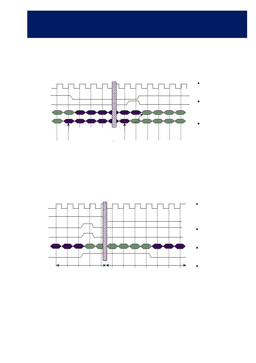
PIXEL DATA OUTPUT PORT
The decompressed pixel data is output via the PixOut port in
response to the PixOutEnab input to the core. It is
accompanied by a PixOutValid signal which indicates valid
output data. The pixel data is also accompanied by a
PixOutSob signal which, when asserted, marks the first word
in each output 8x8 block of pixel data. The last block of
decoded pixel output data in a scan is accompanied by the
PixOutLast signal.
The PixOutEnab signal can be used to control the flow of the
output blocks on a block per block basis. If PixOutEnab is
asserted and the iDCT module has a block to process then it
will start processing the block and will output it. If
PixOutEnab is de-asserted then the core will finish processing
the current block and if the processing of the next block has
started then it will also be output. Processing will then stop
until PixOutEnab is re-asserted.
Figure 6: Pixel Data Output Interface Timing
DECODED JPEG HEADERS OUTPUT PORT
Image marker data is output from CS6150 via the DecJpg[7:0]
port and is accompanied by a DecJpgAvail signal when valid
data is output on the DecJpg port. The contents of the output
stream from the DecJpg port are controlled by the JpgMask
input which is read when the first byte of the input JPEG
stream is input. If any one of the bits of JpgMask is asserted,
then the SOI and EOI markers are also passed to the DecJpg
port. The output receiving device reads the marker data from
the core by asserting the DecJpgNext signal. This indicates
that the next 8-bit word of marker data can be placed on the
DecJpg port at the rising edge of the clock. If data is not
removed from DecJpg by the reading device then the core will
fill with data and will stop reading the decode stream. The
output from the DecSoiEoi port indicates the start and end of
the image.
Figure 7: Decode JPEG Headers Output Interface Timing
CLK (I)
PixOutEnab (I)
PixOut (O)
PixOutValid (O)
PixOutSob (O)
PixOutLast (O)
0
1
2
62
63
0
1
2
3
62
63
0
PixOutSob associated with the
first pixel of an 8x8 block
1
2
CLK (I)
DecJpg (O)
DecJpgAvail (O)
DecJpgNext (I)
DecSoiEoi[1:0] (O)
Marker data read as
DecJpgAvail is asserted
Marker data held as
DecJpgNext is low
ff
D8
ff
D9
10
01
8
CS6150
Motion JPEG Decoder
PARAMETER DATA OUTPUT PORT
The PValue[15:0] output port enables the various parameters
extracted from the input JPEG data stream and currently used
by the core to be read. The data available on the PValue port is
for information only and does not contain control signals for
the decoder core. The desired parameter is selected using the
input PType. These parameters are only available after the
SigSOS output has been asserted.
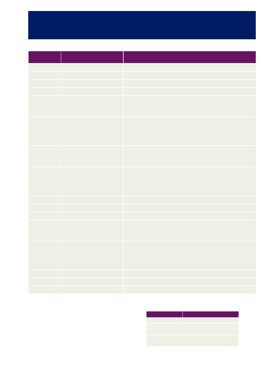
Figure 8 shows the functional timing for the parameter
interface. It shows the following points:
Figure 8: Parameter (PValue) Output Timing
TEST DATA OUTPUT PORT
For diagnostic purposes the output test data port TData[10:0]
enables either the DCT coefficients or the quantized DCT
coefficients to be displayed, selected by the value of TType.
The test port operates independently of the normal system
operation. Test data output is accompanied by two status
signals [TSOS, TSOB] which indicate the first output byte of
the first 8x8 block of the test data (TSOS) and the first output
byte of each 8x8 block of test data (TSOB).
Figure 9 illustrates the functional timing for the test data
output interface. It shows the following points:
Figure 9: Test Data Output Timing
CLK (I)
PValid (O)
SigSOS (O)
PValue (O)
PType (I)
Invalid Loading Headers
as SigSOS is not asserted
The PValid output is asserted
when valid coding parameters
are available on the PValue
output port.
The SigSOS output (asserted
for one cycle and indicating the
start of an image scan) indicates
that the parameter values for a
particular scan are available.
The PType input specifies the
type of parameter required. It
causes the appropriate value
of the parameter to be clocked
out on the PValue port.
CLK (I)
TType (I)
TSOS (O)
TSOB (O)
TData (O)
TValid (O)
0
1
QDCT Output
DCT Output
63
The TType input specifies the
type of test data required. This
can be either DCT coefficients,
set to 0 , or quantized DCT
coefficients, set to 1 . It is active
on a cycle per cycle basis.
The TSOS output is asserted for
one cycle to indicate the first out-
put byte of the first 8x8 block of
the test data.
The TSOB output is asserted
for one cycle to indicate the first
output byte of each 8x8 block
of test data.
The TValid output is asserted
when valid test data is available
on the TData output port.

9
TM
STATUS REGISTERS
The status register flags (DecFlags[7:0]) indicate the current
state of the CS6150 operation. When an error is detected
during the coding process, the compression process is
suspended and the CS6150 waits until a reset process is
invoked by signal RSTn or CLR. The individual bits are set to
zero at reset and active high to indicate an error condition as
defined in Table 4.
ENCODING PARAMETER BUS
The decoding parameter bus (PValue[15:0]) is a 16-bit port
used to output various parameters extracted from the input
data stream and currently used by the core. The 4-bit selector
input (PType[3:0]) determines which internal parameters are
displayed on the parameter bus as per Table 5.
The data available on the PValue port does not contain control
signals used by the CS6150. Many of the values however can
be used to control other logic instantiated around the CS6150,
i.e. the FX and FY parameters (PType 0x0 and 0x1) could be
used to control a block to raster converter.
Table 4: Status Register Pin Definitions
BIT
NAME
DESCRIPTION
7
DecHfError
Set when an undefined Huffman table symbol is referenced during decoding
6
CtlError
Set when an invalid SOF parameter is detected. This includes detecting:
A sample precision which is not equal to 8-bit
The horizontal size of the image set to zero
The number of components in a frame set to zero
Any of the horizontal or vertical sampling ratios set to be greater than 4
The quantization table ID greater than 3
Set when an invalid SOS parameter is detected. This includes detecting:
A reference to an undefined Huffman or quantization table
The number of components in a scan to be zero or more than 4
More than 10 blocks in an MCU
Incorrect SOS fixed parameter settings (these should be as follows:Ss=0
Se=63 AhAl=0)
Set when DecFlags[7] is set
Set when there is a mismatch between the DNL segment input to the core and
the number of lines in the input image which have already been decoded
5
HtError
Set when an invalid DHT segment is detected. This includes detecting:
An all one Huffman code
An invalid Huffman Table class (this should be `0' for DC tables and `1' for
AC tables)
An invalid Huffman table identifier (this should be in the range 0 to 3)
The L value limit has been exceeded (this should be 12 for a DC table
and 162 for an AC DC table)
4
QtError
Set when an invalid DQT segment is detected. This includes detecting:
A zero quantization coefficient
An invalid quantization level precision (this should be set to zero for
baseline JPEG)
An invalid quantization table identifier (this should be in range 0 to 3)
3
DecError
Set when anything other than a JPEG marker is input
Set when any of DecFlags[7:4] are set
Set when any SOF marker is detected other than SOF0
Set if incomplete Huffman or quantization definition is detected
2
IDctInProg
Set when the first sample of the first 8x8 block is output into the core and de-
asserted when the last pixel of the last block of the scan is output
1
DecInProg
For each scan this signal is asserted after the SigSOS signal has been output
from the core and is deasserted when decoding is complete. It indicates that the
core is in the decoding state.
0
JpgInProg
Set when core starts to process input data (JpgIn) and de-asserted when decod-
ing has been completed i.e. when the last pixel of last block of the image is output
10
CS6150
Motion JPEG Decoder
JPEG MASK BUS
The marker data on the decoded JPEG headers output port is
determined by setting the bit-wise value at the inputs on
JpgMask[4:0] according to Table 6. The listed segments will be
output if present in the decode stream.
Table 5: Parameter Bus Definitions
PTYPE
(Decimal Value)
PValue Output
(bit position [15:0])
DESCRIPTION
0
FY[15:0]:
FY
Number of lines in frame
1
FX[15:0]
FX
Number of lines in image
2
00_YMCU[13:0]
YMCU Number of MCUs in Y direction of current scan
3
00_XMCU[13:0]
XMCU Number of MCUs in X direction of current scan
4
Cs0[7:0]_Tq0[1:0]_V0[2:0]_H0[2:0]
Cs0
Identifier for the first scan component
Tqo
Quantization table identifier for the first scan component
V0
Vertical sampling factor for the first scan component. Values = 1-4
H0
Horizontal sampling factor for the first scan component. Values = 1-4
5
Cs1[7:0]_Tq1[1:0]_V1[2:0]_H1[2:0]
Cs1
Identifier for the second scan component
Tq1
Quantization table identifier for the second scan component
V1
Vertical sampling factor for the second scan component, undefined if NS
(number of scans) < 2
H1
Horizontal sampling factor for the second scan component, undefined if
NS < 2
6
Cs2[7:0]_Tq2[1:0]_V2[2:0]_H2[2:0]
Cs2
Identifier for the third scan component
Tq2
Quantization table identifier for the third scan component
V2
Vertical sampling factor for the third scan component, undefined if NS < 3
H2
Horizontal sampling factor for the third component, undefined if NS < 3
7
Cs3[7:0]_Tq3[1:0]_V3[2:0]_H3[2:0]
Cs3
Identifier of the fourth component
Tq3
Quantization table identifier for the fourth scan component
V3
Vertical sampling factor for the fourth scan component, undefined if
NS < 4
H3
Horizontal sampling factor for the fourth scan component, undefined if
NS < 4
8
CsH[15:0]
Number of rows in current scan
9
CsV[15:0]
Number of columns in current scan
10
DRI[15:0]
Restart Interval
11
000_HMAX[2:0]_VMAX[2:0]_
MCUBLK[3:0]_NS[2:0]
HMAX Maximal horizontal sampling factor in frame
VMAX Maximal vertical sampling factor in frame
MCUBLK Number of blocks per MCU of the current scan from 1-10
NS
Number of scan components in current scan, 1-4
12
VHM3[3:0]_VHM2[3:0]_VHM1[3:0[_
VHM0[3:0]
VHM0 Number of blocks of first component in MCU. Defined as V0*H0 where
V0 and H0 are the vertical and horizontal sampling factors for the first
scan component if NS < 1. Otherwise = 1
VHM1 V0*H0 + V1*H1, undefined when NS < 2
VHM2 V0*H0 + V1*H1 + V2*H2, undefined when NS < 3
VHM3 V0*H0 + V1*H1 + V2*H2 + V3*H3, undefined when NS < 4
13
Reserved
14
Reserved
15
Reserved
Table 6: JpgMask Settings
BIT
DATA MARKER
4
SOF, SOS, DNL
3
COM, APP
2
DRI
1
DQT
0
DHT
11
TM
TIMING CHARACTERISTICS
Most inputs and outputs to the CS6150 are registered and fully synchronous. Full pin descriptions and conditional timing
behavior for non-registered pins are given in the CS6150 Databook. Example timing characteristics for the CS6150 are given in
Table 7. Timing characteristics are technology dependent and will vary by instantiation as signal loading in the target system
determines final timing.
CS6150TK: All values relect pre-layout estimated timing. Wireloading conditions use "Conservative" model supplied by library vendor and worst case commercial operating conditions.
AVAILABILITY AND IMPLEMENTATION INFORMATION
ASIC CORES
For applications that require the high performance, low cost and high integration of an ASIC, Amphion delivers a series of ASIC
cores that are pre-optimized by Amphion experts to a targeted silicon technology. Choose from off-the-shelf versions of the
CS6150 available for many popular ASIC and foundry silicon supplier technologies, or Amphion can port the CS6150 to a
technology of your choice.
* Performance figures based on silicon vendor design kit information. ASIC performance is pre-layout using vendor-provided statistical wire loading information under the following condition:
(T
j
=125
o
C, V
cc
- 10%).
**Logic gates do not include clock circuitry
Consult you local AMPHION representative for product specific preformance information, current availability, and lead times on ASIC core porting.
PROGRAMMABLE LOGIC CORES
For ASIC prototyping or for projects requiring the fast time to market of a programmable logic solution, Amphion delivers
programmable logic core solutions that offer the silicon-aware performance tuning found in all Amphion products, combined
with the rapid design times offered by today's leading programmable logic solutions.
* Performance represents core only under worst case commercial conditions. Does not include timing effect of external logic and I/O circuitry.
Table 7: CS6150 Timing Characteristics
SYMBOL
DESCRIPTION
CONDITION
VALUE
COMMENT
t
cyc
Clock cycle rate
Worst case
8.0 ns
Positive edge triggered
t
su
Input port set-up time
max
2.8 ns
t
h
Input port hold time
max
0 ns
t
co
Output port clock to out-
put timing
max
2.8 ns
All registered outputs
t
skew
Clock skew
max
200 ps
Synthesis Value, final skew is design dependent
Table 8: CS6150 Programmable Logic Cores
PRODUCT
ID#
SILICON
VENDOR
PRODUCT
NAME/PROCESS
PERFORMANCE*
(Msamples/sec)
LOGIC GATES**
MEMORY AREA
AVAILABILITY
CS6150TM
TSMC
130 nm using Artisan
standard cell libraries
185
60k
9.6 kbits
Now
CS6150TK
TSMC
180 nm using Artisan
standard cell libraries
125
72k
9.6 kbits
Now
CS6150KJ
Amkor
250 nm using Synopsys
standard cell libraries
95
71k
9.6 kbits
Now
Table 9: CS6150 Programmable Logic Cores
PRODUCT
ID#
SILICON
VENDOR
PROGRAMMABLE
LOGIC PRODUCT
PERFORMANCE*
(Msamples/sec)
DEVICE RESOURCES
USED (LOGIC)
DEVICE RESOURCES
USED (MEMORY)
AVAILABILITY
CS6150AB
Altera
Apex-II FPGA
38
8779 LEs
5 ESB
Now
CS6150AC
Altera
Stratix FPGA
48
8800LEs
3 ESBs
Now
CS6150X2
Xilinx
Virtex-II FPGA
41
3422 slices
5 block RAMs
9MULTs
Now

CS6150
Motion JPEG Decoder
TM
Virtual Components for the Converging World
CORPORATE HEADQUARTERS
Amphion Semiconductor Ltd
50 Malone Road
Belfast BT9 5BS
Northern Ireland, UK
Tel:
+44.28.9050.4000
Fax: +44.28.9050.4001
EUROPEAN SALES
Amphion Semiconductor Ltd
CBXII, West Wing
382-390 Midsummer Boulevard
Central Milton Keynes
MK9 2RG England, UK
Tel:
+44 1908 847109
Fax:
+44 1908 847580
WORLDWIDE SALES & MARKETING
Amphion Semiconductor, Inc
2001 Gateway Place, Suite 130W
San Jose, CA 95110
Tel:
(408) 441 1248
Fax: (408)
441
1239
CANADA & EAST COAST US SALES
Amphion Semiconductor, Inc
Montreal
Quebec
Canada
Tel:
(450) 455 5544
Fax:
(450) 455 5543
Web: www.amphion.com
Email: info@amphion.com
© 2001-02 Amphion Semiconductor Ltd. All rights reserved.
Amphion, the Amphion logo,"Virtual Components for the Converging World", are trademarks of Amphion Semiconductor Ltd. All others are the property of their
respective owners.
12
08/02 Publication #: DS6150 v1.3
ABOUT AMPHION
Amphion (formerly Integrated
Silicon Systems) is the leading
supplier of speech coding, video/
image processing and channel
coding application specific silicon
cores for system-on-a-chip (SoC)
solutions in the broadband,
wireless, and mulitmedia markets
SALES AGENTS
SPS-DA PTE LTD
21 Science Park Rd
#03-19 The Aquarius
Singapore Science Park II
Singapore 117628
T el:
+65 774 9070
Fax:
+65 774 9071
SPINNAKER SYSTEMS INC
Hatchobori SF Bldg. 5F 3-12-8
Hatchobori, Chuo-ku
T oky o 104-0033 Japan
Tel:
+81 3 3551 2275
Fax:
+81 3 3351 2614
V oy ageur T echnical Sales Inc
6205 Airport Road
Building A, Suite 300
Toronto, Ontario
Canada L4V1E1
T el:
(905) 672 0361
Fax:
(905) 677 4986
JASONTECH, INC
Hansang Building, Suite 300
Bangyidong 181-3, Songpaku
Seoul Korea 138-050
T el:
+82 2 420 6700
Fax:
+82 2 420 8600
Phoenix T echnologies Ltd
3 Gavish Street
Kfar -Saba, 44424
Israel
T el:
+972 9 7644 800
Fax:
+972 9 7644 801