 | –≠–ª–µ–∫—Ç—Ä–æ–Ω–Ω—ã–π –∫–æ–º–ø–æ–Ω–µ–Ω—Ç: CS6210TK | –°–∫–∞—á–∞—Ç—å:  PDF PDF  ZIP ZIP |
TM
Virtual Components for the Converging World
Amphion continues to expand its family of application-specific cores
1
See http://www.amphion.com for a current list of products
CS6210
Discrete Wavelet Transform
The CS6210 Forward Discrete Wavelet Transform Core is designed to provide high performance solutions for
still image and video compression systems where a high quality frame-based coding approach is required. This
highly integrated application specific silicon core is fully compliant with the JPEG2000 image coding system. The
CS6210 core provides features vital for high-end and emerging imaging applications and is particularly suited
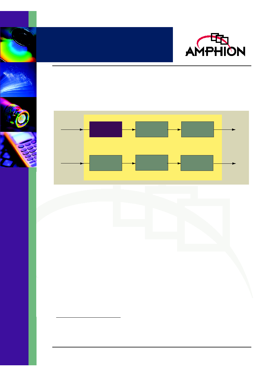
for the compression systems that receive and transfer image data in a serial manner. Figure 1 represents the
application of the wavelet transform core in a JPEG2000 codec system.
Figure 1: JPEG2000 Codec System
Wavelet
Synthesis
Quantization
DeQuantization
Entropy
Encoding
Entropy
Decoding
Wavelet
Analysis
Source
Image Data
Compressed
Image Data
Source
Image Data
Compressed
Image Data
FEATURES
Fully compliant with IS15444-1/ ITU-T Recom-
mendation T.800-1: JPEG 2000 Image Coding
System
Fully configurable tile dimensions (height and
width up to 128x128)
Configurable level of wavelet decomposition
(up to 5 levels)
Continuous processing for 128x 128 blocks
for up to 5 levels of decomposition
Near continuous processing for other block
sizes
Core memory requirements (~ 50KB)
1
High performance (~150MSamples/Sec)
Single sample per cycle processing
High arithmetic precision
KEY METRICS
Logic area: 55K Gates
Memory: 50KB
Input clock: >150MHz
APPLICATIONS
Digital still camera
Remote digital video and PC-based video cap-
turing
High definition DVB
Digital video recording
Video editing for professional broadcasting
1. Actual performance is dependant on target process technology and libraries

2
CS6210
Discrete Wavelet Transform
CS6210 FUNCTIONAL DESCRIPTION
The CS6210 2-D FDWT core provides a row-based wavelet
transform for the 9-7 irreversible and 5-3 reversible wavelet
filter bank. The architecture has been designed to allow very
close to a single sample/clock cycle processing for all tile
dimensions and enables high data throughput.
The FDWT transforms a signal into detail and approximation
components by filtering it through a filter bank comprising
high-pass and low-pass filters. The CS6210 core uses the filter
coefficients corresponding to the irreversible bi-orthogonal 9-7
wavelet function as well as the reversible bi-orthogonal 5-3
wavelet function. These wavelet functions are those specified
in Part 1 of the JPEG 2000 Image Coding Standard. Both have
attractive properties in terms of image compression and
treatment of boundary effects. The FDWT normally comprises
multiple levels of filter bank decomposition, where the low-
pass output 'level' is iterated a number of times through the
wavelet filter bank. Therefore, a signal can be separated into
multiple sub-bands, each providing selective information on
the signal.
CORE OPERATION
The CS6210 core is initialized on power-up by an
asynchronous active low pulse at the RSTn port or a
synchronous active high pulse at the CLR port. Data is burst
into the core row-wise with the first data value of every row
being accompanied by an InpValid signal. The core accepts 16-
bit input data and produces a 16-bit transformed output. The
position of the data in the 16-bit input specifies the precision
and the number of guard bits. Figure 2 represents the CS6210
overview diagram.
Tiled image data is input row-wise in raster order into the
CS6210 core via the InpDat port. The core is designed such
that only the first 5 rows of a tile need to be stored internally
in order to begin data processing. These are held in the Input
Memory. Within the CS6210 a periodic symmetric extension
policy is employed to manage data on the boundaries of tiles.
The horizontal and vertical transformation and sub-sampling
of the data are achieved using a combination of two wavelet
processors, VWP (Vertical Wavelet Processor) and HWP
(Horizontal Wavelet Processor). Following level 1
decomposition of the input data the LL1, HL1, LH1, and HH1
sub-bands are produced. The HL1, LH1, and HH1 are directly
output from the core on the WavOut port. The LL sub-band
from the current level of decomposition is fed into the
Feedback Memory. When sufficient lines of data have been
stored, the processing of a higher level of decomposition may
commence. These values are multiplexed with the data stored
in the Input Memory, at the input of Vertical Wavelet
Processor. The LH, HH and HL outputs for all levels are
scheduled to the WavOut output port as soon as the
Horizontal Wavelet Processor generates them. A principle
sub-block of the core is the data scheduler that stores the data
produced by Vertical Wavelet Processor in appropriate
registers. The data in these registers is then read by the
Horizontal Wavelet Processor to produce the desired sub-
band sequence at the WavOut port. The LL1 sub-band is
further decomposed into sub-bands and each of these are
interleaved in the output data stream. Within each sub-band
the coefficients are output in raster order. The WavSb and
WavLvl indicate the sub-band and level of the current data at
the WavOut port. The sub-band outputs corresponding to a
three level decomposition on a 128x128 tile are shown in
Figure 3.
Figure 2: CS6210 Overview Diagram
MUX
Vertical Wavelet
Processor
(VWP)
Input Memory
(128x16x12)
Input Data
InpDat
Horizontal
Wavelet
Processor
(HWP)
Wavelet
Coefficient
WavOut
16
16
Feedback Memory
(128x16x12)
16

3
TM
Figure 3: Wavelet Subband Coefficients produced for a 128x128 tile
Latency in the Design
The latency in the CS6210 core is dependent on the tile
dimensions and the latency through the filters in VWP and
HWP. However, for higher decomposition levels, the filter
latency becomes negligible in comparison with the width of
the tile. Various latency conditions at different levels of
decomposition are shown in Table 1.
Note
: Tile dimensions are bounded by BlockWidth=128 and
BlockHeight=128, these parameters are defined at the ports
and read at the start of the tile.
Continuous Processing
The core allows continuous processing of 128x128 tiles. This
means that whenever one BlockHeight number of rows are
completed, the InpRdy will be asserted and the next tile can
commence in tandem with InpValid signal. The BlockHeight
and BlockWidth parameters do not need to be changed as
long as the tile size does not change. To process different tile
dimensions, the data from the existing tile needs to be
completely flushed out of the core, new parameters for
BlockHeight and BlockWidth specified at the port and the
new tile can then commence. The core may wait for a few
cycles before two consecutive tiles are read for tile sizes other
than 128x128. This will depend on the BlockWidth and
BlockHeight parameters as well as the number of levels
specified at NumLvls port.
Computational Accuracy
The core uses 16-bit data path architecture. A typical 8-bit
level shifted input data is left-shifted by 4-bits and sign
extended to make 16-bits. The 4 MSB in this case act as the
guard bits. However, the core can take in any 16-bit input and
produce DWT. The filter coefficients used in the computation
of wavelet transform have ten-bit accuracy. The outputs from
the filter are rounded to produce 16-bits. The internal
wordlength allocation in the core ensures that there is no
overflow in wavelet computation as well as meeting the
accuracy requirements for the JPEG 2000 standard.
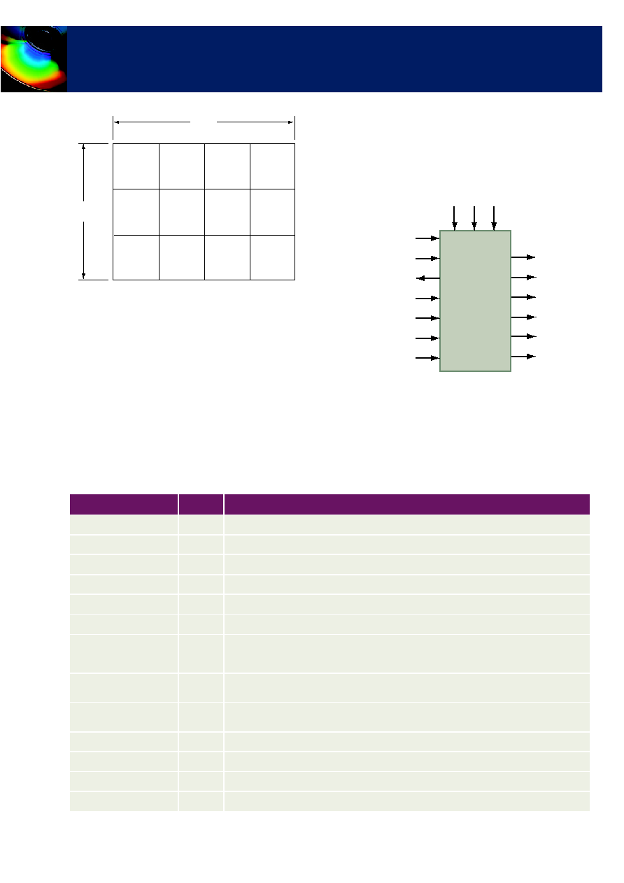
FDWT on Larger Images
The JPEG 2000 standard allows larger images to be segregated
into tiles. These tiles of maximum dimension 128x128 can be
individually processed through the CS6210. The core is also
capable of transforming any tile size below 128x128 pixels and
thus can transform any image size in accordance with the
JPEG 2000 standard. An example of tile components in a
464x346 image is shown in Figure 4. Each of the 128x128 tiles
as well as 80x90 tile, 80x128 tile and 90x128 tile can be sent
through the CS6210 core in any order to produce DWT of the
entire image.
3
1
4
6
2
5
9
7
10
8
HH1
LH1
HL1
HH2
HL2
HL3
HH3
LL3
LH3
LH2
0 1 2 ...
16 17...
15 0 1 2 ...
16 17...
15 0 1 2 ...
32 33...
31 0 1 2 ...
64 65...
63
0 1 2 ...
32 33...
31
0 1 2 ...
32 33...
31
0 1 2 ...
64 65...
63
0 1 2 ...
64 65...
63
Table 1: Latency Requirement for Different Decomposition
Levels
Decomposition Level
Latency
1
5 x BlockWidth
2
14 x BlockWidth
3
32 x BlockWidth
4
68 x BlockWidth
5
140 x BlockWidth
4
CS6210
Discrete Wavelet Transform
Figure 4: Tile Components in an Image
CS6210 SYMBOL
AND PIN DESCRIPTION
Table 2 describes the input and output ports (shown
graphically in Figure 5) of the CS6210 core. Unless otherwise
states, all signals are active high and bit (0) is the least
significant bit.
Figure 5: CS6210 Symbol
12
12
12
80
12
12
12
80
464
12
12
90
12
12
90
34
InpDat[15:0]
InpValid
InpRdy
Mode53
NumLvls[2:0]
BlockWidth[7:0]
BlockHeight[7:0]
WavOut[15:0]
WavVal
WavLvl[2:0]
WavSb[1:0]
WavProg
WavEnd
CS6210
DWT Core
CLK CLR RSTn
Table 2: FDWT Interface Signal Definitions
Signal
I/O
Description
CLK
Input
Clock, rising edge active
RSTn
Input
Asynchronous reset (power on reset)
CLR
Input
Synchronous reset
InpDat [15:0]
Input
Sample data input port
InpValid
Input
Active high indicates a valid input pixel at InpDat port
InpRdy
Output
Active high indicates that the DWT core is ready to accept the next input row
Mode53
Input
Selects the wavelet filters to be used for transformation. A high input indicates 5-3 fil-
ters a low indicates 9-7 filters. Although this signal is read at the beginning of every
tile, the same filters are commonly used for the DWT computation of an entire image
WavOut [15:0]
Output
Wavelet coefficient. The output coefficients are burst out in blocks of 4 i.e.
HL,LH,HL,LL
WavVal
Output
Active high indicates a valid wavelet coefficient output data at WavOut port - asserted
for each WavOut value
NumLvls [2:0]
Input
Number of levels of wavelet decomposition - maximum 5
BlockWidth [7:0]
Input
Tile Width
BlockHeight [7:0]
Input
Tile Height
WavLvl [2:0]
Output
The level of current output

5
TM
WavSb [1:0]
Output
The sub-band of current output
WavEnd
Output
Active High pulse, asserted for one clock cycle, indicates that complete wavelet coef-
ficients for one tile have been produced. This pulse is produced at the end of every
tile that is processed
WavProg
Output
Active high signal, remains asserted from the reading of first sample of the first tile to
the assertion of WavEnd pulse corresponding to the last output of the last tile. The
processing parameters can be changed whenever WavProg is not asserted. This sig-
nal can also be used for clock-gating
Table 2: FDWT Interface Signal Definitions
Signal
I/O
Description
6
CS6210
Discrete Wavelet Transform
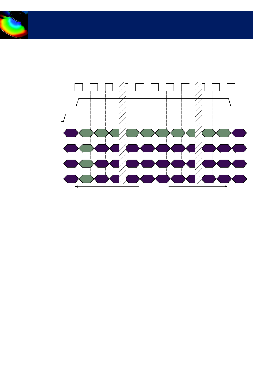
TIMING DIAGRAMS
DATA INPUT TIMING
Figure 6 illustrates the functional timing diagrams for CS6210 data input interface.
Figure 6: Data Input Interface Timing Diagram
The data is input to the core via the InpDat[15:0] port. This interface operates synchronously, reading a data sample at the rising
edge of every clock cycle. Signal InpValid must be asserted coincident with the first valid data sample in each row of the tile. The
following diagrams illustrate the wavelet coefficient output timing for different decomposition levels.
126
127
One Tile Input Period
0
128
128
0
0
2
126
127
1
2
1
CLK
InpValid
InpRdy
InpDat [15:0]
NumLvls [2:0]
BlockWidth [7:0]
BlockHeight [7:0]
7
TM
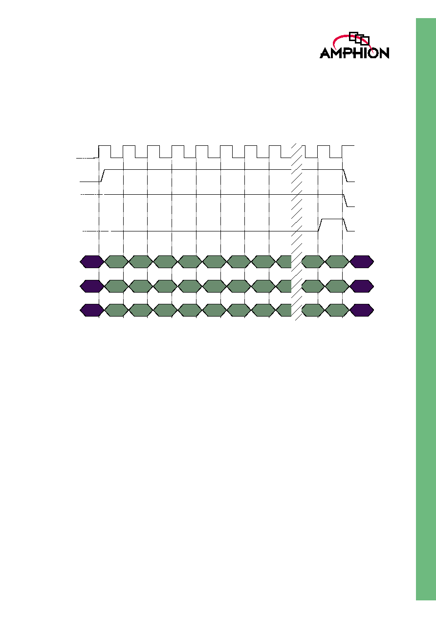
OUTPUT TIMING FOR ONE LEVEL
The transformed wavelet coefficients are output from the core via the WavOut[15:0] port. The wavelet coefficient output interface
operates synchronously, outputting a burst of four wavelet coefficients (subband values 00, 01, 10, 11 correspond to LL, HL, LH,
HH respectively). The valid output wavelet coefficients are accompanied by the WavVal signal. The subband and level of output
data are indicated by WavSb and WavLvl signals respectively.
Figure 7: Output Timing Diagram for One Level of Analysis
00
01
01
10
11
00
10
11
10
11
000
000
000
000
000
000
000
000
000
000
CLK
WavVal
WavProg
WavEnd
WavOut [15:0]
WavSb [1:0]
WavLvl [2:0]
8
CS6210
Discrete Wavelet Transform
OUTPUT TIMING FOR TWO LEVELS
In the case of having a multiple level of wavelet decomposition, the WavLvl signal indicates the analysis level of the data
available at the output. The WavVal indicates a valid output data and WavSb indicates HL, LH, HH for all levels except for the
highest level output. The output of the highest level also provides the LL data.
Figure 8: Output Timing Diagram for Two Levels of Analysis
01
01
10
11
01
00
10
11
01
10
000
001
000
000
000
001
001
001
000
000
CLK
WavVal
WavProg
WavEnd
WavOut [15:0]
WavSb [1:0]
WavLvl [2:0]

9
TM
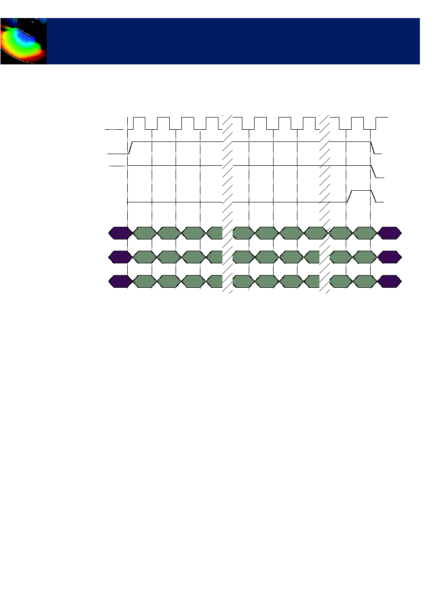
OUTPUT TIMING FOR MULTIPLE TILES
In the case of an input comprising multiple tiles, the output is processed continuously or with breaks, depending upon the tile
dimensions. The WavVal indicates a valid wavelet output corresponding to WavSb and WavLvl outputs. The WavEnd signal
indicates that the current tile has ended and the subsequent output data corresponds to the next input tile.
Figure 9: Output Timing Diagram for Multiple Tiles
Tile 1
Completed
Tile 2
Completed
01
01
10
00
10
00
10
11
00
10
000
000
000
001
001
000
000
001
001
001
CLK
WavVal
WavProg
WavEnd
WavOut [15:0]
WavSb [1:0]
WavLvl [2:0]

10
CS6210
Discrete Wavelet Transform
AVAILABILITY AND IMPLEMENTATION INFORMATION
ASIC CORES
For applications that require the high performance, low cost and high integration of an ASIC, Amphion delivers application
specific silicon cores that are pre-optimized to a targeted silicon technology by Amphion experts.
Consult your local Amphion representative for product specific performance information, current availability of individual
products, and lead times on ASIC core porting.
* Performance figures based on silicon vendor design kit information. ASIC design is pre-layout using vendor-provided statistical wire loading information, under the following
condition: (T
J
= 125∫C, V
cc
-10%)
**Logic gates do not include clock circuitry
PROGRAMMABLE LOGIC CORES
For ASIC prototyping or for projects requiring the fast time-to-market of a programmable logic solution, Amphion delivers
programmable Logic solutions that offer the silicon-aware performance tuning combined with the rapid design times offered by
today's leading programmable logic solutions.
*Performance represents core only under worst case commercial condition. Does not include timing effect of external logic and I/O circuitry
Table 3: CS6210 ASIC Cores
PRODUCT
ID
SILICON
VENDOR
PRODUCT NAME/
PROCESS
PERFORMANCE*
(MSAMPLES/SEC)
LOGIC**
GATES
MEMORY
AVAILABILITY
CS6210TK
TSMC
180 nm using Artisan
standard Cell libraries
151
55K
50KB
Now
Table 4: CS6210 Programmable Logic Cores
PRODUCT
ID
SILICON
VENDOR
PROGRAMMABLE
LOGIC PRODUCT
PERFORMANCE*
(MSAMPLES/SEC)
LOGIC
USED
MEMORY
USED
AVAILABILITY
CS6210AA
Altera
Apex20KE
47
7381 LEs
24 ESBs
Now
CS6210XE
Xilinx
VirtexE-8
55
3784
SLICES
24 BRAMs
Now

CS6210
Discrete Wavelet Transform
TM
Virtual Components for the Converging World
CORPORATE HEADQUARTERS
Amphion Semiconductor Ltd
50 Malone Road
Belfast BT9 5BS
Northern Ireland, UK
Tel:
+44.28.9050.4000
Fax: +44.28.9050.4001
EUROPEAN SALES
Amphion Semiconductor Ltd
CBXII, West Wing
382-390 Midsummer Boulevard
Central Milton Keynes
MK9 2RG England, UK
Tel:
+44 1908 847109
Fax:
+44 1908 847580
WORLDWIDE SALES & MARKETING
Amphion Semiconductor, Inc
2001 Gateway Place, Suite 130W
San Jose, CA 95110
Tel:
(408) 441 1248
Fax:
(408) 441 1239
CANADA & EAST COAST US SALES
Amphion Semiconductor, Inc
Montreal
Quebec
Canada
Tel:
(450) 455 5544
Fax: (450)
455
5543
Web: www.amphion.com
Email: info@amphion.com
© 2001-02 Amphion Semiconductor Ltd. All rights reserved.
Amphion, the Amphion logo, "Virtual Components for the Converging World", are trademarks of Amphion Semiconductor Ltd. All others are the property of their
respective owners.
11
04/02 Publication #: DS6210 v1.1
ABOUT AMPHION
Amphion (formerly Integrated
Silicon Systems) is the leading
supplier of speech coding, video/
image processing and channel
coding application specific silicon
cores for system-on-a-chip (SoC)
solutions in the broadband,
wireless, and mulitmedia markets
SALES AGENTS
SPS-DA PTE LTD
21 Science Park Rd
#03-19 The Aquarius
Singapore Science P ark II
Singapore 117628
T el:
+65 774 9070
Fax:
+65 774 9071
SPINNAKER SYSTEMS INC
Hatchobori SF Bldg. 5F 3-12-8
Hatchobori, Chuo-ku
T oky o 104-0033 Japan
Tel:
+81 3 3551 2275
Fax:
+81 3 3351 2614
V oy ageur T echnical Sales Inc
1 Rue Holiday
T our Est, Suite 501
P oint Claire, Quebec
Canada H9R 5N3
T el:
(905) 672 0361
Fax:
(905) 677 4986
JASONTECH, INC
Hansang Building, Suite 300
Bangyidong 181-3, Songpaku
Seoul Korea 138-050
T el:
+82 2 420 6700
Fax:
+82 2 420 8600
Phoenix T echnologies Ltd
3 Gavish Street
Kfar -Saba, 44424
Israel
T el:
+972 9 7644 800
Fax:
+972 9 7644 801