 | –≠–ª–µ–∫—Ç—Ä–æ–Ω–Ω—ã–π –∫–æ–º–ø–æ–Ω–µ–Ω—Ç: CS6350 | –°–∫–∞—á–∞—Ç—å:  PDF PDF  ZIP ZIP |

TM
Virtual Components for the Converging World
Amphion continues to expand its family of application-specific cores
1
See http://www.amphion.com for a current list of products
CS6350
High Performance IDCT
At the heart of many video decompression systems is the inverse discrete cosine transform (IDCT) function. The
JPEG-compliant CS6350 IDCT provides a high-performance reconstruction of a video waveform from its
constituent frequency components. Capable of processing one symbol per cycle at sustained data rates of over
217 mega-samples/sec
1
in an ASIC implementation and 80 mega-samples/sec in FPGA,
the CS6350 forms the
heart of a high-performance video decompression solution. The CS6350 DCT is available in both ASIC and
programmable logic versions that have been handcrafted by Amphion to deliver high performance with low-
power and minimal silicon area.
Figure 1: Typical Digital Video Processing Channel Containing the CS6350
DISPLAY
DEVICE
PAL/NTSC
DECODER
COLOR
SPACE
CONVERTER
STRIP BUFFER
RASTER-BLOCK
CONVERTER
IDCT
FEATURES
High Performance IDCT Core
ASIC/FPGA/PLD versions available
Continuous one symbol per cycle processing
capability
Other data precisions available on request
High performance (217 M samples/second)
1
Highly portable firm core
Ideal solution for JPEG
Fully compliant with baseline JPEG Standard
ISO/IEC 10918-1/2
KEY METRICS AND
SPECIFICATIONS
Logic:
39k gates
Memory:
1K bit RAM
Max Frequency:
217 MHz
APPLICATIONS
JPEG systems
Scanners
Copiers
Remote digital video
1. Actual performance is dependent on the ASIC libraries used and ASIC process targeted
2
CS6350
High Performance IDCT
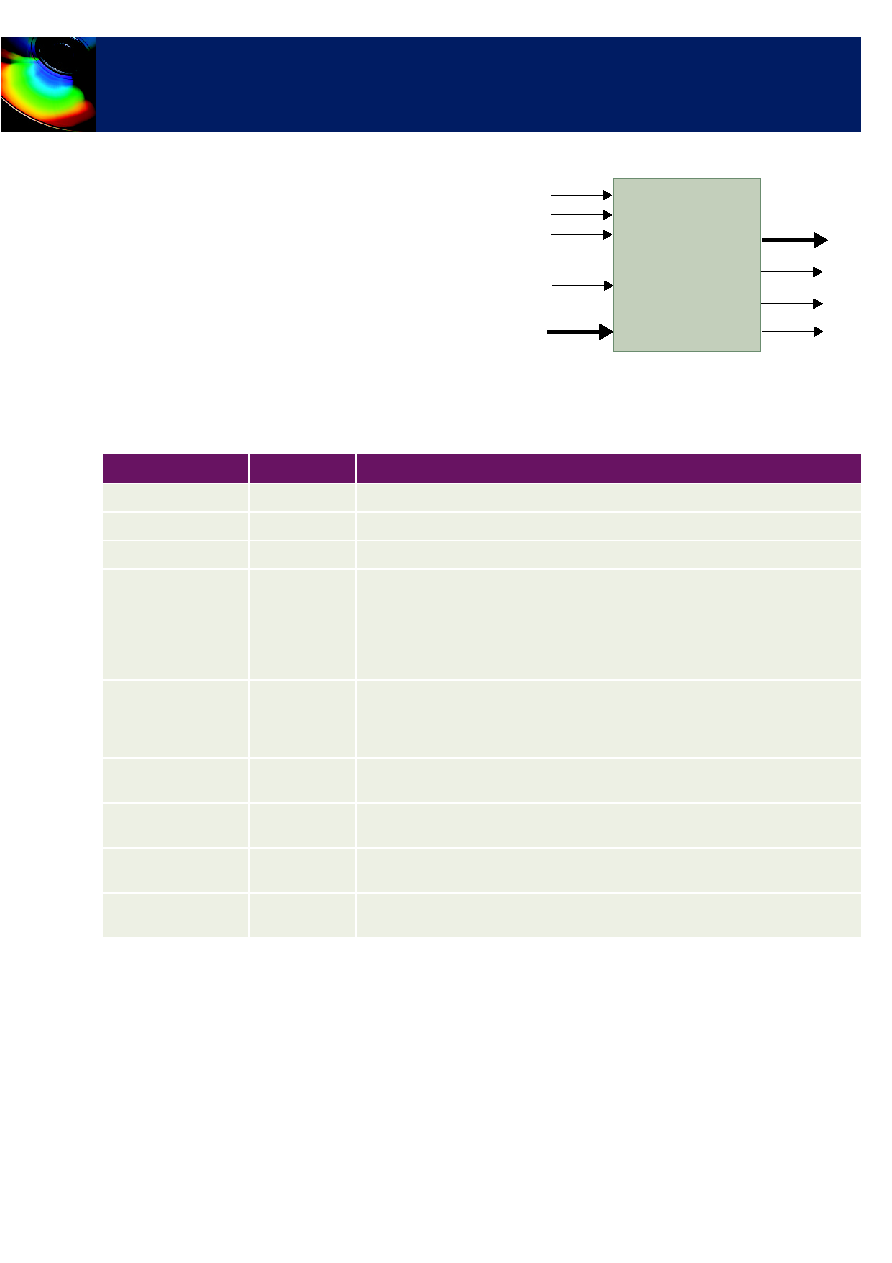
PIN/PORT DESCRIPTION
Table 1 describes the input and output ports (shown
graphically in Figure 2) for the CS6350 High Performance
IDCT core. Unless otherwise stated, all signals are active high
and bit (0) is the least significant bit.
Figure 2: CS6350 Core Pinouts
PixOut[7:0]
PixOutSob
IDctRdy
PixOutValid
CLR
RSTn
CLK
DctStrb
DctCoef[10:0]
CS6350
IDCT
Table 1: I/O Signal Descriptions
Signal
I/O
Description
CLK
Input
Clock signal
CLR
Input
Synchronous reset signal
RSTn
Input
Active low, asynchronous reset signal
DctStrb
Input
Signal to indicate to the core that the first sample in a 8x8 block is available for pro-
cessing. Active '1' pulse for one CLK time period. DctStrb can be left '1' after first
assertion for continuous processing of data blocks. However, in case of any gaps
between successive blocks, it must be asserted along with first data sample of a
block. Re-assertion of DctStrb within a 8x8 block segment has no effect on process-
ing.
DctCoef [10:0]
Input
11-bit wide DCT coefficient input port. The data is burst in on block by block basis. If
the data sequence is corrupted for any reason, the port will continue to read 64 ele-
ments of an 8x8 block and then wait for the assertion of DctStrb to read next valid
data block.
PixOut [7:0]
Output
8-bit wide pixel data output port. The data is burst out on block by block basis in col-
umn-major order.
PixOutSob
Output
DC flag. Associated with the first output of an 8x8 block, can also be regarded as
the start signal of the block. Active '1' pulse for one CLK period.
IDctRdy
Output
Active '1' signal indicates that the core can read a new block of coefficients. It goes
to a '0' state whenever DctStrb has been asserted.
PixOutValid
Output
Active '1' to indicate the availability of a valid output data block. It will remain contin-
uously asserted as long as valid data is available at the PixOut port.

3
TM
FUNCTIONAL DESCRIPTION
The DCT is a transform that converts a signal into its
constituent frequency components as represented by a set of
coefficients. For an image, this transform is performed on a 2
dimensional array of samples, resulting in a 2 dimensional
array of coefficients. The data input into the core and output
from the core takes place as a block of 8x8 samples. In the case
of IDCT, the input to the core is the block of transformed
coefficients and the output is the original pixels.
The transform can be performed as a one or two stage
process. The two-stage process performs the transform as two
separate one-dimensional transforms. This results in a set of
intermediate results being produced which require storage
and further processing.
The CS6350 performs its function as two 1-dimensional
transforms, using row-column decomposition, with the
intermediate results being stored in the transpose memory. A
block diagram of the core, showing the main interfaces and
functional blocks is shown in Figure 3 with the blocks
described in the following sections.
Figure 3: IDCT Block Diagram
The core is initialized on power-up by an asynchronous active
low pulse at RSTn port or a synchronous active high pulse at
CLR port. Data is burst into the core in blocks of 64, with the
first data value being accompanied by DctStrb signal. The core
accepts 11-bit DCT coefficient inputs and produces an 8-bit
pixel data output.
STAGE 1
This processing stage comprises a multiplier-accumulator unit
as well as a Cosine lookup tables for respective IDCT
computations. The input to this stage is the data DctCoef from
the input port. The output from this processing stage is
rounded to 15-bits to provide the desired computational
accuracy and passed onto the transpose memory.
STAGE 2
This processing stage comprises a multiplier-accumulator unit
as well as a Cosine lookup tables for respective IDCT
computations. The input to this stage is the data stored in the
Transpose Memory by stage 1. This stage, similar to stage1,
performs a 1-D IDCT and provides the final 8-bit output at
PixOut port.
TRANSPOSE MEMORY
This 64x15 dual-port RAM stores intermediate results after
first stage of processing. The data is written into the memory
in a row-major order and read from it in a column-major
order, which is effectively a transposition. Along with the
transposition of data, it provides input to the processing stage
for the second stage of IDCT processing
ALGORITHM
The core implements the 2-D IDCT as two one-dimensional
operations as defined by the following equations. The results
from the first stage are stored in the transpose memory.
DCT
IDCT
where
ACCURACY
The Amphion implementation performs the transform in two
stages with the first stage results being stored in the Transpose
memory. The width of this memory, 15-bit, controls the
number of fractional bits stored and hence influences the
accuracy of the final result. The other factor that controls the
accuracy is the number of fractional bits, i.e. 14-bits, used
when calculating the cosine coefficients.
PixOutValid
IDctRdy
PixOut
DctStrb
DctCoef
CLK
CLR
RSTn
Stage 1
CS6350
Transpose
Memory
Stage 2
PixOutSob
S u
( )
C u
( )
2
------------
s x
( )
2x 1
+
(
)u
16
---------------------------
cos
x
0
=
7
=
S u
( )
C u
( )
2
------------
S u
( )
2x 1
+
(
)u
16
---------------------------
cos
x
0
=
7
=
C u
( )
1
2
------- for u=0
=
C u
( ) 1 for u>0
=
s x
( ) = 1-D sample value
S u
( ) = 1-D DCTcoefficient
4
CS6350
High Performance IDCT
DCT OPERATION
The processing may begin by supplying 8x8 blocks of 11-bit
DCT coefficients to the DctCoef port, with the first sample of
the block being coincident with the DctStrb.
The IDCT is performed as two one dimensional IDCTs, with
the intermediate results being stored in the Transpose
memory. In this high performance IDCT, two processing
blocks comprising multipliers and accumulators are used for
both the one dimensional computation stages of 2D-IDCT. The
output from the first stage is stored in the Transpose Memory
and appropriately supplied to the second stage. Once the
complete 8x8 block has been processed, the IDctRdy signal is
asserted to indicate that the core can now read the next block
of data. The start of each output block is indicated by the
assertion of PixOutSob signal which coincides with the first
output sample at the PixOut port.
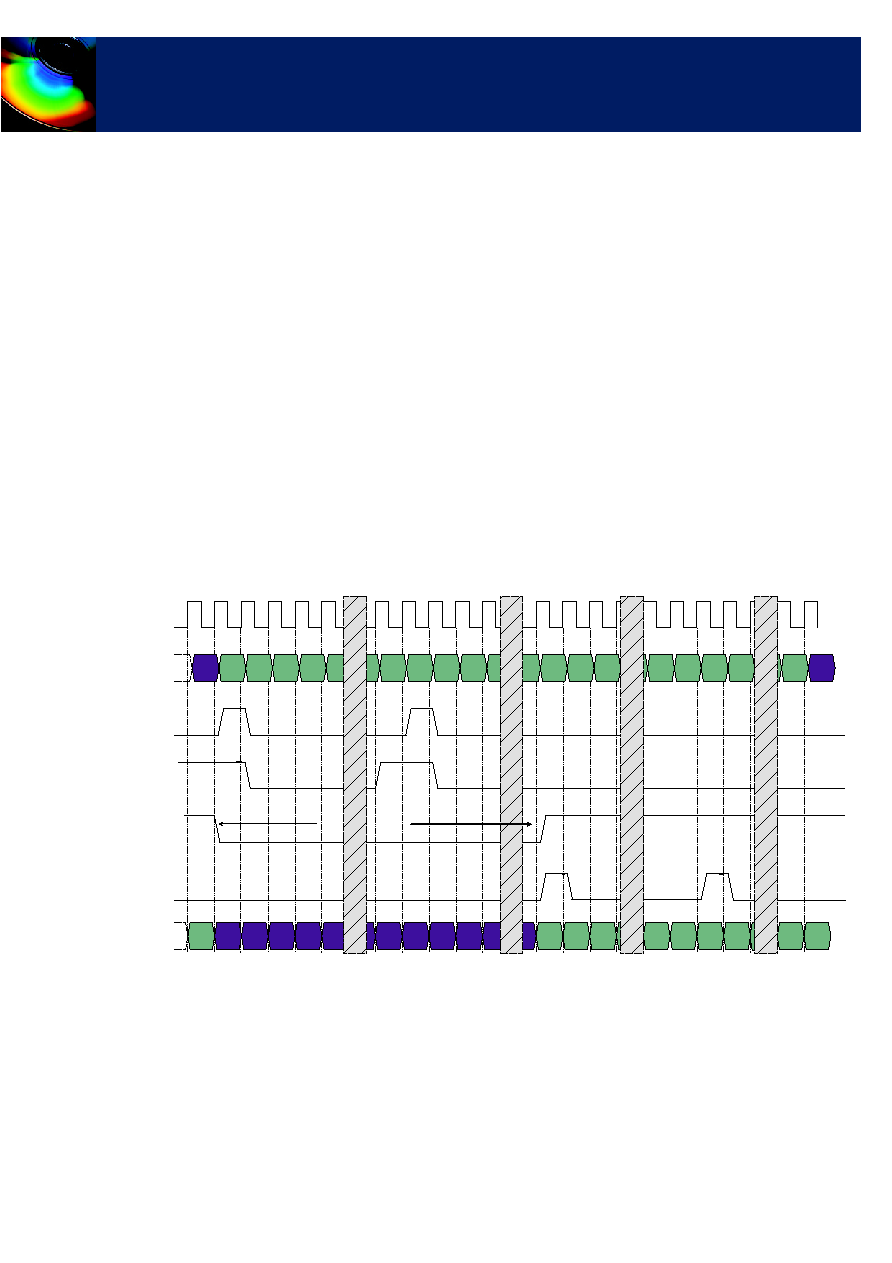
LATENCY IN THE DESIGN
There is a latency of 83 clock cycles before which the first
output sample appears at the output. Consequently, there is a
similar latency of 83 CLK cycles between the last input data
and the last output data. The latency is depicted in the
functional timing diagram in Figure 4.
I/O FUNCTIONAL TIMING DIAGRAMS
The timing diagram in Figure 4 depicts the activities at
various ports for IDCT operation. The start of the block is
marked by DctStrb pulse which remains active for one clock
period. After 83 clock cycles, i.e. system latency, the
PixOutSob goes high to mark the start of new output data
block at PixOut port. The processing of two contiguous input
blocks can be delayed by delaying the assertion of DctStrb
signal. The IDctRdy signal, which shows that the core is ready
for processing, will remain asserted until the core starts to
read a new data block. The core will start processing the data
when DctStrb is asserted. All input signals are sampled with
CLK and all outputs are updated with CLK. Any gaps at the
input DctCoef port are replicated at the output PixOut port
after the latent period. The PixOutValid pin remains asserted
at '1' as long as a valid data is available at the PixOut port. The
core is capable of performing consecutive IDCT with or
without gaps between successive input blocks.
Figure 4: IDCT Timing
0
1
2
3
63
0
1
2
19
20
19
20
63
63
0
1
2
0
1
CLK
DctCoef
PixOut
63
DctStrb
IDctRdy
PixOutSob
PixOutValid
System Latency

5
TM
AVAILABILITY AND IMPLEMENTATION INFORMATION
ASIC CORES
For applications that require the high performance, low cost and high integration of an ASIC, Amphion delivers a series of
multimedia ASVCs that are pre-optimized by Amphion experts to a targeted silicon technology. Choose from off-the-shelf
versions of the CS6300 family available for many popular ASIC and foundry silicon supplier technologies or Amphion can port
the CS6300 to a technology of your choice.
*Performance figures based on silicon vendor design kit information. ASIC design is pre-layout using vendor-provided statistical wire loading information, under the
following condition: (T
J
= 125
o
C, V
CC
-10%)
**Logic gates do not include clock circuitry
Consult you local Amphion representative for product specific performance information, current availability of individual products, and lead times on ASIC core porting.
PROGRAMMABLE LOGIC CORES
For ASIC prototyping or for projects requiring the fast time to market of a programmable logic solution, Amphion provides
programmable logic core solutions that offer the silicon-aware performance tuning found in all Amphion products, combined
with the rapid design times offered by today's leading programmable logic solutions.
*Performance represents core only under worst case commercial condition. Does not include timing effect of external logic and I/O circuitry.
Table 2: CS6350 ASIC Cores
PRODUCT ID
SILICON
VENDOR
PROCESS TECHNOLOGY
PERFORMANCE*
LOGIC
GATES**
MEMORY
AREA
AVAILABILITY
CS6350TK
TSMC
180 nm using Artisan standard
cell libraries
217
39k
0.08mm
2
Now
Table 3: CS6350 Programmable Logic Cores
PRODUCT ID
SILICON
VENDOR
PROGRAMMABLE
LOGIC PRODUCT
PERFORMANCE*
(MSAMPLES/
SEC)
DEVICE RESOURCES
USED (LOGIC)
DEVICE RESOURCES
USED (MEMORY)
AVAILABILITY
CS6350AE
Altera
Apex 20KE
83
3434 LEs
1 ESB
Now
CS6350XE
Xilinx
Virtex-E
86
1662 Slices
1 block RAM
Now

CS6350
High Performance IDCT
TM
Virtual Components for the Converging World
CORPORATE HEADQUARTERS
Amphion Semiconductor Ltd
50 Malone Road
Belfast BT9 5BS
Northern Ireland, UK
Tel:
+44.28.9050.4000
Fax: +44.28.9050.4001
EUROPEAN SALES
Amphion Semiconductor Ltd
CBXII, West Wing
382-390 Midsummer Boulevard
Central Milton Keynes
MK9 2RG England, UK
Tel:
+44 1908 847109
Fax:
+44 1908 847580
WORLDWIDE SALES & MARKETING
Amphion Semiconductor, Inc
2001 Gateway Place, Suite 130W
San Jose, CA 95110
Tel:
(408) 441 1248
Fax:
(408) 441 1239
CANADA & EAST COAST US SALES
Amphion Semiconductor, Inc
Montreal
Quebec
Canada
Tel:
(450) 455 5544
Fax:
(450) 455 5543
Web: www.amphion.com
Email: info@amphion.com
© 2001-02 Amphion Semiconductor Ltd. All rights reserved.
Amphion, the Amphion logo,"Virtual Components for the Converging World", are trademarks of Amphion Semiconductor Ltd. All others are the property of their
respective owners.
6
04/02 Publication #: DS6350 v1.1
ABOUT AMPHION
Amphion (formerly Integrated
Silicon Systems) is the leading
supplier of speech coding, video/
image processing and channel
coding application specific silicon
cores for system-on-a-chip (SoC)
solutions in the broadband,
wireless, and mulitmedia markets
SALES AGENTS
SPS-DA PTE LTD
21 Science Park Rd
#03-19 The Aquarius
Singapore Science P ark II
Singapore 117628
T el:
+65 774 9070
Fax:
+65 774 9071
SPINNAKER SYSTEMS INC
Hatchobori SF Bldg. 5F 3-12-8
Hatchobori, Chuo-ku
T oky o 104-0033 Japan
Tel:
+81 3 3551 2275
Fax:
+81 3 3351 2614
V oy ageur T echnical Sales Inc
1 Rue Holiday
T our Est, Suite 501
P oint Claire, Quebec
Canada H9R 5N3
T el:
(905) 672 0361
Fax:
(905) 677 4986
JASONTECH, INC
Hansang Building, Suite 300
Bangyidong 181-3, Songpaku
Seoul Korea 138-050
T el:
+82 2 420 6700
Fax:
+82 2 420 8600
Phoenix T echnologies Ltd
3 Gavish Street
Kfar -Saba, 44424
Israel
T el:
+972 9 7644 800
Fax:
+972 9 7644 801