TM
Virtual Components for the Converging World
Amphion continues to expand its family of application-specific cores
1
See http://www.amphion.com for a current list of products
CS6650
High Definition MPEG-2 Video Decoder
The CS6650 high-definition MPEG2 decoder is designed to provide high performance solutions for a broad range
of motion image applications. This highly integrated application specific core is developed for standard
definition video, compliant with ISO/IEC 13818-2 (MPEG2) and capable of decoding video streams up to 4:2:2
Profile at High Level (422@HL). The CS6650 is equally at home in mainstream consumer applications, decoding
4:2:0 bitstreams at High or Main Level (MP@HL) and can also decode MPEG1 (ISO/IEC 11172-2) bitstreams. The
CS6650 is available in ASIC netlists that have been handcrafted by Amphion for optimal performance while
minimizing power consumption and silicon area.
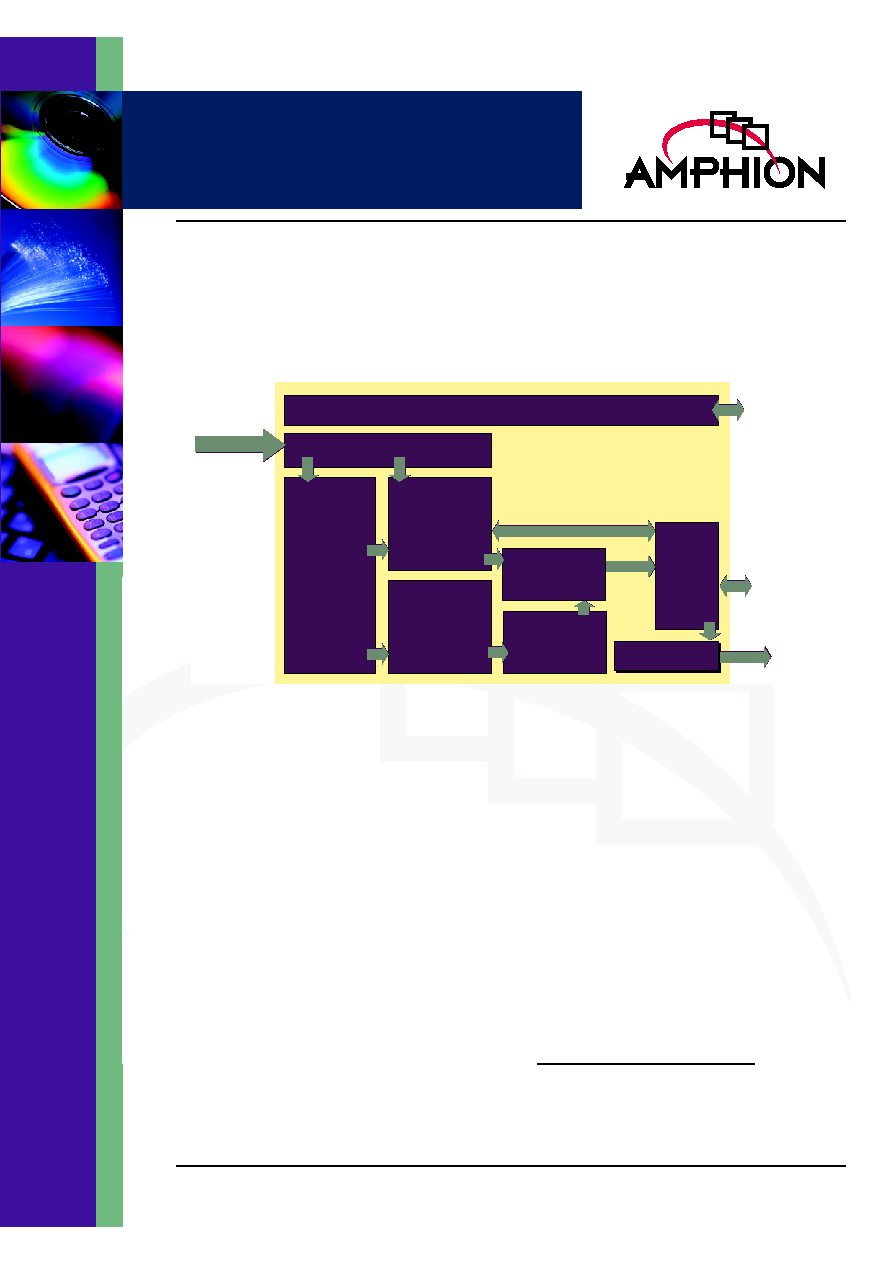
Figure 1: CS6650 Overview Diagram
Host Interface
Video Stream Parser
Input Video
Data Stream
Host
Microprocessor
Frame
Store
SDRAMs
Output
Picture
Data
Motion
Compensation
Variable
Length Code
Decoder
Run Level
Decoder
&
Inverse
Quantization
Picture
Reconstruction
iDCT
Picture DMA
Frame Store
Interface
DECODER FEATURES
Supports progressive scan and interlaced
streams
ISO/IEC 13818-2 (H.262) Compliant
-
MP@ML through 4:2:2@HL
-
Decodes ISO/IEC11172-2 (MPEG1) Con-
strained Parameter bitstreams
High performance solution for high data rate
MPEG2 decoding
-
Supports input bit rates up to 300Mbit/sec
-
Real time decode and display of 4:2:2@HL
Supports all ATSC and HDTV defined resolu-
tions and frame rates
Bitstream error detection and recovery
Glueless interface to external SDRAM
Capable of standalone stream decoding or
host CPU controlled operation
Fully synchronous design with host shut-
down and restart control
Ease of integration
-
� Tapeout-ReadyTM
-
� ScanReadyTM
KEY METRICS AND
SPECIFICATION
Logic:
105k gates
Memory:
-
1.5Kbytes (internal)
-
128 MBit (external), 2M x 32 PC133 SDRAM
Logic area:
1.3mm
2
1
Input clock:
133 MHz
APPLICATIONS
Digital cable and satellite set-top decoder box
for ATSC and HDTV
DVD - standard and high definition
PC video hardware accelerator
Studio 4:2:2 editing or production
1. Calculation assumes logic density of 90k gates/mm
2
; does not include
area of on-chip RAM

2
CS6650
High Definition MPEG-2 Video Decoder
CS6650 FUNCTIONAL DESCRIPTION
The CS6650 core is a highly integrated MPEG2 video decoder suitable for a wide range of video applications. The CS6650 accepts
the input video elementary stream as aligned bytes from conditional access decryption, transport stream demulti-plexer, or
similar source. The maximum average input bit rate is 300Mbits/sec. The core can operate in a default mode on an input stream
without the intervention of a host CPU. In this mode pictures will be decoded from the video stream and output in correct
display order. A host CPU has access to a full range of information and control to manipulate the behavior of the decoder to
permit audio/video synchronization, pan and scan and letterbox conversion, and various trick modes.
The output from the core is provided by a highly configurable pixel stream DMA (Direct Memory Access) engine. This engine
allows adjustable output video component sequencing and provides external logic with control over the display of the picture.
To meet the bandwidth requirements of 422@HL decoding, a bank of two dedicated SDRAM chips is used. These SDRAM chips
are commodity 64Mbit PC133 SDRAMs in 2Mx32 configuration.
FUNCTIONAL BLOCK OVERVIEW
VIDEO STREAM PARSER
The Video Stream Parser unit extracts various encoding para-
meters from the input video stream and any requested user
specific data contained within the stream, such as closed-
caption or teletext data. This information is contained in
headers at each layer of the stream and may be used
throughout the rest of the decoding and reconstruction
process. Selected user data is stored to buffer space and made
available to the host CPU. Having removed header
information from the stream, the Video Stream Parser unit
passes the variable length encoded picture data to the Variable
Length Code (VLC) Decoder unit. A range of parameters
describing the overall stream and the picture currently being
decoded is made available to the rest of the decoder.
VARIABLE LENGTH CODE DECODER
The Variable Length Code Decoder unit decodes the
Huffman-style variable length encoded picture data. The
outputs of this unit include the Discrete Cosine Transform
(DCT) block run-level information for the Inverse DCT (iDCT)
unit and decoded macroblock motion vectors for the motion
compensation unit as well as a number of information fields
describing the section of the picture currently being decoded.
These decoded fields are made available to the rest of the
decoder.
RUN-LEVEL DECODER & INVERSE
QUANTIZATION
The output run-level information from the VLC decoder is
converted into complete blocks of 64 quantized DCT
coefficients by the Run-Level decoder. These coefficients are
passed to the Inverse Quantizer for conversion back to actual
DCT coefficients. To perform this, the Inverse Quantizer keeps
track of a number of tables and scale factors, all extracted from
the input video stream.
INVERSE DCT
This high performance unit performs the inverse quantization
of 8x8 DCT-encoded Y, Cr and Cb pixel blocks. This key unit is
capable of streaming data through continuously,
transforming, every 64 clock cycles, an entire block of 8x8
DCT coefficients into an 8x8 block of pixel samples or
estimated sample corrections.
MOTION COMPENSATION
Where the video data is encoded as an estimate using
previous pictures and a set of corrections, the Motion
Compensation unit forms the estimated pixel values. The
Motion Compensation unit takes decoded motion vectors
from the Variable Length Code Decoder unit and translates
them into row and column coordinates within the pictures
from which the estimations are being made. The reference
samples for these coordinates are requested from the Frame
Store Interface and the resulting pixels combined where
necessary to form the estimated values for the block being
decoded.
PICTURE RECONSTRUCTION
The Picture Reconstruction unit combines decoded pixels or
corrections from the iDCT unit with the estimated pixels from
the Motion Compensation Unit and writes the resulting pixels
to the Frame Store, ready for subsequent display or reference.
FRAME STORE INTERFACE
The Frame Store is required for the storage of the two
reference pictures used in the MPEG2 algorithm to form the
estimated pixels. It also stores the frame currently being
decoded and another frame currently being displayed. This
allows the decoding and the display operations to be
decoupled making audio/video synchronization simpler to
maintain.
3
TM
The Frame Store is implemented using two SDRAM chips
which are commodity PC133 64Mbit parts, each with 2Mx32
organization. The memory interface runs at 133MHz and can
be directly connected to the SDRAM chips using suitable
pads.
The Frame Store SDRAM Interface handles the mapping of
pixel read and write requests from the Motion Compensation,
Picture Reconstruction and Picture DMA units into linear
memory addresses. Additionally, the host interface can access
the memory banks. Arbitration between the various accessing
units and memory transaction queues are all maintained by
the SDRAM Interface.
PICTURE DISPLAY DMA
The Picture Display DMA has a double-byte output interface
which can carry Y, Cr or Cb pixel data. Y and Cr or Cb data
can be output simultaneously as 16-bit wide values or
sequentially as four separate bytes. For 4:2:0 video streams the
Picture Display DMA unit will upsample the chrominance
vertically to provide a 4:2:2 output. The Display DMA engine
has the capability to be programmed by the host CPU to
display only a certain portion of the picture or, in stand-alone
mode, will display the entire coded picture.
A number of handshake signals are provided on the Picture
Display DMA interface to allow the external logic to control
the timing of the pixel output stream and to control the end of
the current scan row or picture display. Outputs indicate to
the external logic the nature of the pixel being currently
driven; the end of row and end of picture flags are available to
allow, for example, sync pulse generation.
HOST INTERFACE
When the CS6650 is operating with the assistance of a host
CPU, a number of additional features can be accessed. All
interfacing between the host and the CS6650 is performed
through the Host Interface unit. This unit allows read/write
access to all the internal control, status and video stream
parameter registers contained within the decoder.
The Host Interface also provides a simple 32-bit read/write
access to the Frame Store SDRAM. Normally, the areas of the
SDRAM used for storage of picture data cannot be accessed
by the Host Interface; however, a bypass mode allowing direct
access is provided for system diagnostic tests, etc.
A number of conditions arising from the decoding of the
video stream may require the software on the CPU to be
alerted. An interrupt controller within the Host Interface unit
provides a simple Interrupt Request signal and an interrupt
status and mask register.
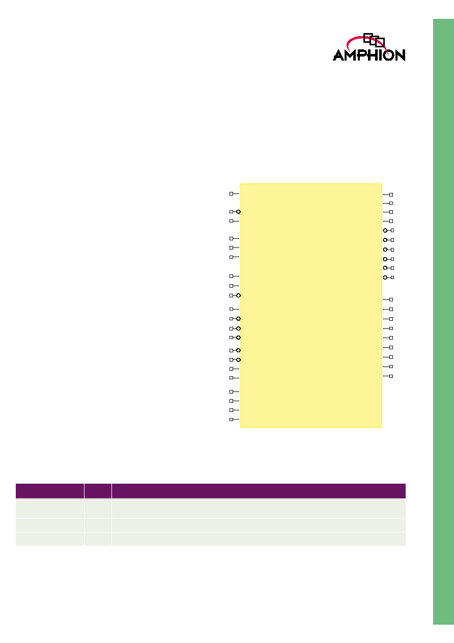
Figure 2: CS6650 Symbol and Pin Description
Clk
SD_DataOut(63:0)
SD_DQM(7:0)
SD_Addr(10:0)
SD_BA(1:0)
P_Data(15:0)
P_DataAvail
P_DataType(3:0)
P_DataStrobe
P_RowDoneOut
P_PicDoneOut
P_RowDoneIn
P_PicDoneIn
P_General(7:0)
SD_notRAS
SD_notCAS
SD_notWE
SD_notCS
notReset
CoreReset
ES_Data(7.0)
ES_Valid
ES_Stall
H_DataOut(31:0)
H_DataIn(31:0)
H_notDatDrv
H_Addr(21:0)
H_notRegCS
H_notWrite
H_notMemRead
H_notMemWrite
H_MemBusy
H_ByteEnable(3:0)
H_MemRdValid
H_MemRdStrb
H_MemWrValid
H_MemWrReady
H_notIRQ
SD_DataIn(63:0)
SD_notDatDrv
Table 1: Global Signals
Signal
I/O
Description
Clk
I
Core Clock. Master clock used for all logic and the external SDRAM interface. This clock should also be
routed to the external SDRAM chips. This clock should be 133 MHz.
notReset
I
Core reset. Asynchronous, active low global core reset
CoreReset
I
Core reset. Synchronous, active high core reset

4
CS6650
High Definition MPEG-2 Video Decoder
Table 2: Input Interface
Signal
I/O
Description
ES_Data[7:0]
I
Elementary Stream Data, byte aligned video elementary stream data from the Conditional Access decryp-
tion unit or transport stream demux. Maximum average input bit rate is 300Mbits/s
ES_Valid
I
Data Valid Strobe. ES_Data is latched on the positive edge of Clk when ES_Valid is asserted, and
ES_Stall is deasserted (see below).
ES_Stall
O
Data Stall. Input data may be bursted into the core at a rate higher than the specified maximum 300Mbit/
sec. In this case the core will indicate that it temporarily cannot receive any more data by assertion of
ES_Stall. ES_Data will not be latched while ES_Stall is asserted.
Table 3: Picture Output Interface
Signal
I/O
Description
P_Data[15:0]
O
Picture Output Data. Output from the decoded picture display DMA engine. Contains either Y, Cr or Cb, as
indicated by P_DataType. In 16 bit mode, the upper 8 bits carry Y and the lower 8 bits carry either Cr or Cb
as indicated by P_DataType.
P_DataStrobe
I
Data Valid Strobe. Indicates that the external logic will consume the current P_Data on the next rising edge
of clock. This signal is also used to qualify the P_RowDoneIn and P_PicDoneIn signals.
P_DataAvail
O
Picture Data Available. Indicates that the DMA engine has been configured and is running and that
P_Data carries a valid picture sample.
P_DataType[3:0]
O
Picture Data Type, indicates the type of sample on P_Data. the bottom two bits carry the component iden-
tification as follows: 00 = Y1, 01 = Y2, 10 = Cb, 11 = Cr. The top two bits carry display frame/field informa-
tion as follows: 00 = progressive, 01 = undefined, 10 = top field, 11 = bottom field.
P_RowDoneIn
I
Last Pixel In Row. This input can be used to terminate a row scan and move on to the next. This may be
used with pan and scale external logic. This input is ignored in certain DMA engine configurations. Should
be asserted for the last byte of the pixel sample group � the engine will move to the next row after the last
component for the group is taken.
P_PicDoneIn
I
Last Pixel In Picture. Indicates to the DMA engine that the display of the picture is complete at the end of
the current pixel. The engine will revert to idle mode. This input is ignored in certain DMA engine configu-
rations. Should be asserted for the last byte of the pixel sample group � the engine will stop after the last
component for the group is taken.
P_RowDoneOut
O
Last Pixel In Row. This output can be programmed to indicate the last component of the last pixel of the
row. This requires correct configuration of the DMA engine row length register.
P_PicDoneOut
O
Last Pixel In Picture. This output can be programmed to indicate the last component of the last pixel of the
picture. This requires correct configuration of the DMA engine vertical size register.
P_General[7:0]
O
General Outputs. These outputs directly reflect the programmed value in the DMA General Output regis-
ter. They can be used by the host CPU to inform the display logic of specific display parameters such as
PAL/NTSC encoding information etc.

5
TM
Table 4: Frame Store Interface
Signal
I/O
Description
SD_DataIn[63:0]
I
SDRAM Data Input. Read data input from the external SDRAM
SD_DataOut[63:0]
O
SDRAM Data Output. Write data output to the external SDRAM
SD_notDatDrv
O
SDRAM Data Drive. Active low enable signal for SDRAM data bus tristate drivers. Driven low when
SD_DataOut should be placed on the bus.
SD_Addr[10:0]
O
SDRAM Address Bus. Carries row or column addresses or commands to the external SDRAM.
SD_BA[1:0]
O
SDRAM Bank Address. Indicates selected bank for the current SDRAM command.
SD_DQM[7:0]
O
SDRAM DQ Mode. Used to control burst transfers of data to/from the SDRAM.
SD_notRAS
O
SDRAM Row Address Strobe. Strobes a row address or command into the SDRAM.
SD_notCAS
O
SDRAM Column Address Strobe. Strobes a column address or command into the SDRAM.
SD_notWE
O
SDRAM Write Enable. Indicates to the SDRAM that a write command is required.
SD_notCS
O
SDRAM chip select. Initiates a command to the SDRAM.
Table 5: Host Interface
Signal
I/O
Description
H_DataIn[31:0]
I
Host Data Input. Host Write data into the core.
H_DataOut[31:0]
O
Host Data Output. Host Read data from the core.
H_notDatDrv
O
Host Data Drive. Indicates that a read is active. This can be used to control external tristate drivers if
required. Active low.
H_Addr[21:0]
I
Host Address. Used to select a register for read/write, or a Frame Store SDRAM word to be accessed.
H_notRegCS
I
Host Chip Select. Active low enable signal controls all host register accesses.
H_notWrite
I
Host Write Select. It is asserted when H_notRegCS is asserted, the register addressed by H_Addr will
have the value on H_DataIn assigned to it on the rising edge of the Clk signal, if the appropriate byte write
enable signal is also asserted. If it is deasserted when H_notRegCS is asserted then a register read is ini-
tiated and H_DataOut will show the selected register's data on the next tick.
H_notIRQ
O
Host interrupt request. Active low output
H_ByteEnable[3:0]
I
Host Byte Write Enables. Used on write accesses to control which bytes in a register or SDRAM word
actually get written.
H_notMemRead
I
Host Memory Read Access. Initiates an SDRAM host read transaction.
H_notMemWrite
O
Host Memory Write Access. Initiates an SDRAM host write transaction.
H_MemBusy
O
Host Memory Interface Busy. Indicates that a memory access transaction is in progress. This can be used
to insert read wait states and to stall for posted writes to complete.
H_MemRdValid
O
Host Memory Read Data Valid. Indicates that the read data is available on the H_DataOut port.
H_MemRdStrb
I
Host Memory Read Data Strobe. Indicates that the host will consume the data from the H_DataOut port
on the next rising edge of Clk.
H_MemWrValid
I
Host Memory Write Data Valid. Indicates that the host has placed valid write data on the H_DataIn port.
Note that H_ByteEnable should be valid at the same time as the data.
H_MemWrReady
O
Host Memory Write Data Ready, indicates that the core is ready to consume the data on H_DataIn on the
positive edge of Clk when it is signalled as valid with H_MemWrValid