TM
Virtual Components for the Converging World
Amphion continues to expand its family of application-specific cores
1
See http://www.amphion.com for a current list of products
CS6651
MPEG-2 Video Decoder for FPGA
The CS6651 MPEG2 decoder is designed to provide high performance solutions for a broad range of motion
image applications. This highly integrated application specific virtual component (ASVC) is for standard
definition video, compliant with ISO/IEC 13818-2 (MPEG2) and capable of decoding video streams at the Main
Profile at Main Level (MP@ML). The CS6651 is at home in mainstream consumer applications and can also
decode MPEG1 (ISO/IEC 11172-2) bitstreams. The CS6651 is available for Altera and Xilinx FPGA and has been
handcrafted by Amphion for optimal performance while minimizing power consumption and silicon area.
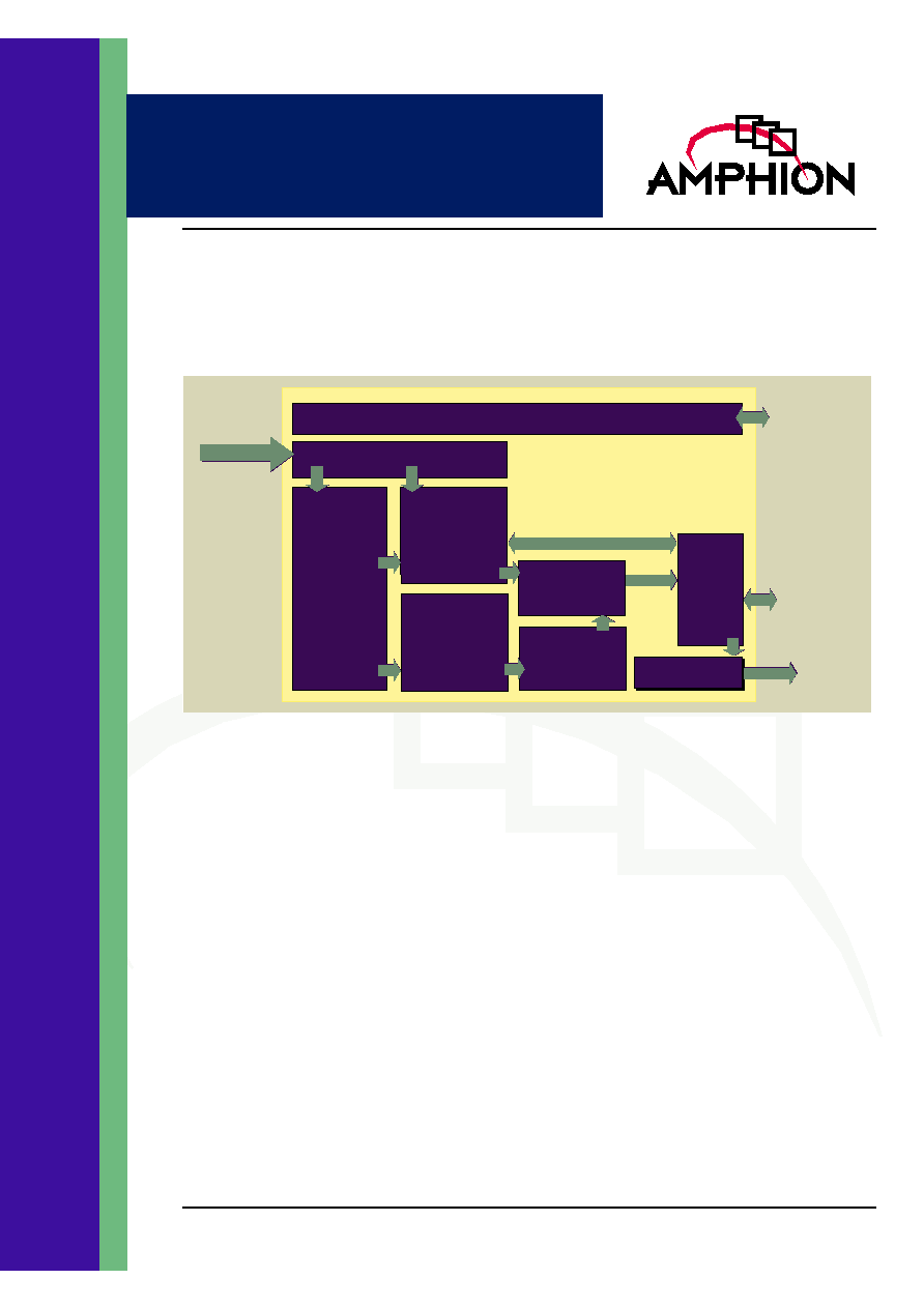
Host Interface
Video Stream Parser
Input Video
Data Stream
Host
Microprocessor
Frame
Store
SDRAMs
Output
Picture
Data
Motion
Compensation
Variable
Length Code
Decoder
Run Level
Decoder
&
Inverse
Quantization
Picture
Reconstruction
iDCT
Picture DMA
Frame Store
Interface
Figure 1: CS6651 Overview Diagram
DECODER FEATURES
Supports progressive scan and interlaced
streams
ISO/IEC 13818-2 (H.262) Compliant
-
MP@ML
-
Decodes ISO/IEC11172-2 (MPEG1) Con-
strained Parameter bitstreams
High performance solution for MPEG2
decoding
-
Supports input bit rates up to 30Mbit/sec
-
Real time decode and display of MP@ML
Supports PAL and NTSC SDTV resolutions
and frame rates
Bitstream error detection and recovery
Glueless interface to external SDRAM
Capable of standalone stream decoding or
host CPU controlled operation
Fully synchronous design with host shut-
down and restart control
APPLICATIONS
Digital cable and satellite set-top decoder box
for SDTV
DVD Players
PC video hardware accelerator

2
CS6651
MPEG-2 Video Decoder for FPGA
CS6651 FUNCTIONAL DESCRIPTION
The CS6651 ASVC is a highly integrated MPEG2 video decoder suitable for a wide range of video applications. The CS6651
accepts the input video elementary stream as aligned bytes from conditional access decryption, transport stream demulti-plexer,
or similar source. The maximum average input bit rate is 30Mbits/sec. The core can operate in a default mode on an input stream
without the intervention of a host CPU. In this mode pictures will be decoded from the video stream and output in correct
display order. A host CPU has access to a full range of information and control to manipulate the behavior of the decoder to
permit audio/video synchronization, pan and scan and letterbox conversion, and various trick modes.
The output from the core is provided by a highly configurable pixel stream DMA (Direct Memory Access) engine. This engine
allows adjustable output video component sequencing and provides external logic with control over the display of the picture.
To meet the bandwidth requirements of MP@ML decoding, a bank of two dedicated SDRAM chips is used. These SDRAM chips
are commodity 64Mbit SDRAMs in 2Mx32 configuration.
FUNCTIONAL BLOCK OVERVIEW
VIDEO STREAM PARSER
The Video Stream Parser unit extracts various encoding para-
meters from the input video stream and any requested user
specific data contained within the stream, such as closed-
caption or teletext data. This information is contained in
headers at each layer of the stream and may be used
throughout the rest of the decoding and reconstruction
process. Selected user data is stored to buffer space and made
available to the host CPU. Having removed header
information from the stream, the Video Stream Parser unit
passes the variable length encoded picture data to the Variable
Length Code (VLC) Decoder unit. A range of parameters
describing the overall stream and the picture currently being
decoded is made available to the rest of the decoder.
VARIABLE LENGTH CODE DECODER
The Variable Length Code Decoder unit decodes the
Huffman- style variable length encoded picture data. The
outputs of this unit include the Discrete Cosine Transform
(DCT) block run-level information for the Inverse DCT (iDCT)
unit and decoded macroblock motion vectors for the motion
compensation unit as well as a number of information fields
describing the section of the picture currently being decoded.
These decoded fields are made available to the rest of the
decoder.
RUN-LEVEL DECODER & INVERSE
QUANTIZATION
The output run-level information from the VLC decoder is
converted into complete blocks of 64 quantized DCT
coefficients by the Run-Level decoder. These coefficients are
passed to the Inverse Quantizer for conversion back to actual
DCT coefficients. To perform this, the Inverse Quantizer keeps
track of a number of tables and scale factors, all extracted from
the input video stream.
INVERSE DCT
This high performance unit performs the inverse quantization
of 8x8 DCT-encoded Y, Cr and Cb pixel blocks. This key unit is
capable of streaming data through continuously; transforming
every 64 clock cycles an entire block of 8x8 DCT coefficients
into an 8x8 block of pixel samples or estimated sample
corrections.
MOTION COMPENSATION
Where the video data is encoded as an estimate using
previous pictures and a set of corrections, the Motion
Compensation unit forms the estimated pixel values. The
Motion Compensation unit takes decoded motion vectors
from the Variable Length Code Decoder unit and translates
them into row and column coordinates within the pictures
from which the estimations are being made. The reference
samples for these coordinates are requested from the Frame
Store Interface and the resulting pixels combined where
necessary to form the estimated values for the block being
decoded.
PICTURE RECONSTRUCTION
The Picture Reconstruction unit combines decoded pixels or
corrections from the iDCT unit with the estimated pixels from
the Motion Compensation Unit and writes the resulting pixels
to the Frame Store, ready for subsequent display or reference.
FRAME STORE INTERFACE
The Frame Store is required for the storage of the two
reference pictures used in the MPEG2 algorithm to form the
estimated pixels. It also stores the frame currently being
decoded and another frame currently being displayed. This
allows the decoding and the display operations to be
decoupled making audio/video synchronization simpler to
maintain.

3
TM
The Frame Store is implemented using two SDRAM chips
which are commodity PC133 64Mbit parts, each with 2Mx32
organization. The memory interface runs at the core speed
and can be directly connected to the SDRAM chip.
The Frame Store SDRAM Interface handles the mapping of
pixel read and write requests from the Motion Compensation,
Picture Reconstruction and Picture DMA units into linear
memory addresses. Additionally, the host interface can access
the memory banks. Arbitration between the various accessing
units and memory transaction queues are all maintained by
the SDRAM Interface.
PICTURE DISPLAY DMA
The Picture Display DMA has a double-byte output interface
which can carry Y, Cr or Cb pixel data. Y and Cr or Cb data
can be output simultaneously as 16-bit wide values or
sequentially as four separate bytes. The Picture Display DMA
unit will upsample the chrominance vertically to provide a
4:2:2 output. The Display DMA engine has the capability to be
programmed by the host CPU to display only a certain
portion of the picture or, in stand-alone mode, will display the
entire coded picture.
A number of handshake signals are provided on the Picture
Display DMA interface to allow the external logic to control
the timing of the pixel output stream and to control the end of
the current scan row or picture display. Outputs indicate to
the external logic the nature of the pixel being currently
driven; and end of row and end of picture flags are available
to allow, for example, sync pulse generation.
HOST INTERFACE
When the CS6651 is operating with the assistance of a host
CPU, a number of additional features can be accessed. All
interfacing between the host and the CS6651 is performed
through the Host Interface unit. This unit allows read/write
access to all the internal control, status and video stream
parameter registers contained within the decoder.
The Host Interface also provides a simple 32-bit read/write
access to the Frame Store SDRAM. Normally, the areas of the
SDRAM used for storage of picture data cannot be accessed
by the Host Interface; however, a bypass mode allowing direct
access is provided for system diagnostic tests, etc.
A number of conditions arising from the decoding of the
video stream may require the software on the CPU to be
alerted. An interrupt controller within the Host Interface unit
provides a simple Interrupt Request signal and an interrupt
status and mask register.
Figure 2: CS6651 Symbol and Pin Description
Clk
SD_Data(63:0)
SD_DQM(7:0)
SD_Addr(10:0)
SD_BA(1:0)
P_Data(15:0)
P_DataAvail
P_DataType(3:0)
P_DataStrobe
P_RowDoneOut
P_PicDoneOut
P_RowDoneIn
P_PicDoneIn
P_General(7:0)
SD_notRAS
SD_notCAS
SD_notWE
SD_notCS
notReset
CoreReset
ES_Data(7.0)
ES_Valid
ES_Stall
H_DataOut(31:0)
H_DataIn(31:0)
H_notDatDrv
H_Addr(21:0)
H_notRegCS
H_notWrite
H_notMemRead
H_notMemWrite
H_MemBusy
H_ByteEnable(3:0)
H_MemRdValid
H_MemRdStrb
H_MemWrValid
H_MemWrReady
H_notIRQ
Table 1: Global Signals
Signal
I/O
Description
Clk
I
Core Clock. Master clock used for all logic and the external SDRAM interface. This clock should also be
routed to the external SDRAM chips. This clock should be 27 MHz.
notReset
I
Core reset. Asynchronous, active low global core reset
CoreReset
I
Core reset. Synchronous, active high core reset

4
CS6651
MPEG-2 Video Decoder for FPGA
Table 2: Input Interface
Signal
I/O
Description
ES_Data[7:0]
I
Elementary Stream Data, byte aligned video elementary stream data from the Conditional Access decryp-
tion unit or transport stream demux. Maximum average input bit rate is 30Mbits/s
ES_Valid
I
Data Valid Strobe. ES_Data is latched on the positive edge of Clk when ES_Valid is asserted, and
ES_Stall is de-asserted.
ES_Stall
O
Data Stall. Input data may be bursted into the core at a rate higher than the specified maximum 30Mbit/
sec. In this case the core will indicate that it temporarily cannot receive any more data by assertion of
ES_Stall. ES_Data will not be latched while ES_Stall is asserted.
Table 3: Picture Output Interface
Signal
I/O
Description
P_Data[15:0]
O
Picture Output Data. Output from the decoded picture display DMA engine. Contains either Y, Cr or Cb, as
indicated by P_DataType. In 16 bit mode, the upper 8 bits carry Y and the lower 8 bits carry either Cr or Cb
as indicated by P_DataType.
P_DataStrobe
I
Data Valid Strobe.
Indicates that the external logic will consume the current P_Data on the next rising edge of clock. This sig-
nal is also used to qualify the P_RowDoneIn and P_PicDoneIn signals.
P_DataAvail
O
Picture Data Available. Indicates that the DMA engine has been configured and is running and that
P_Data carries a valid picture sample.
P_DataType[3:0]
O
Picture Data Type, indicates the type of sample on P_Data. the bottom two bits carry the component iden-
tification as follows: 00 = Y1, 01 = Y2, 10 = Cb, 11 = Cr. The top two bits carry display frame/field informa-
tion as follows: 00 = progressive, 01 = undefined, 10 = top field, 11 = bottom field.
P_RowDoneIn
I
Last Pixel In Row. This input can be used to terminate a row scan and move on to the next. This may be
used with pan and scale external logic. This input is ignored in certain DMA engine configurations. Should
be asserted for the last byte of the pixel sample group � the engine will move to the next row after the last
component for the group is taken.
P_PicDoneIn
I
Last Pixel In Picture. Indicates to the DMA engine that the display of the picture is complete at the end of
the current pixel. The engine will revert to idle mode. This input is ignored in certain DMA engine configu-
rations. Should be asserted for the last byte of the pixel sample group � the engine will stop after the last
component for the group is taken.
P_RowDoneOut
O
Last Pixel In Row. This output can be programmed to indicate the last component of the last pixel of the
row. This requires correct configuration of the DMA engine row length register.
P_PicDoneOut
O
Last Pixel In Picture. This output can be programmed to indicate the last component of the last pixel of the
picture. This requires correct configuration of the DMA engine vertical size register.
P_General[7:0]
O
General Outputs. These outputs directly reflect the programmed value in the DMA General Output regis-
ter. They can be used by the host CPU to inform the display logic of specific display parameters such as
PAL/NTSC encoding information etc.

5
TM
Table 4: Frame Store Interface
Signal
I/O
Description
SD_Data[63:0]
I/O
SDRAM Data Bus. Bidirectional read/write databus to the external SDRAM
SD_Addr[10:0]
O
SDRAM Address Bus. Carries row or column addresses or commands to the external SDRAM.
SD_BA[1:0]
O
SDRAM Bank Address. Indicates selected bank for the current SDRAM command.
SD_DQM[7:0]
O
SDRAM DQ Mode. Used to control burst transfers of data to/from the SDRAM.
SD_notRAS
O
SDRAM Row Address Strobe. Strobes a row address or command into the SDRAM.
SD_notCAS
O
SDRAM Column Address Strobe. Strobes a column address or command into the SDRAM.
SD_notWE
O
SDRAM Write Enable. Indicates to the SDRAM that a write command is required.
SD_notCS
O
SDRAM chip select. Initiates a command to the SDRAM.
Table 5: Host Interface
Signal
I/O
Description
H_DataIn[31:0]
I
Host Data Input. Host Write data into the core.
H_DataOut[31:0]
O
Host Data Output. Host Read data from the core.
H_notDatDrv
O
Host Data Drive. Indicates that a read is active. This can be used to control external tristate drivers if
required. Active low.
H_Addr[21:0]
I
Host Address. Used to select a register for read/write, or a Frame Store SDRAM word to be accessed.
H_notRegCS
I
Host Chip Select. Active low enable signal controls all host register accesses.
H_notWrite
I
Host Write Select. If asserted when H_notRegCS is asserted, the register addressed by H_Addr will have
the value on H_DataIn assigned to it on the rising edge of the Clk signal, if the appropriate byte write
enable signal is also asserted. If de-asserted when H_notRegCS is asserted then a register read is initi-
ated and H_DataOut will show the selected registers data on the next clock cycle.
H_notIRQ
O
Host interrupt request. Active low output
H_ByteEnable[3:0]
I
Host Byte Write Enables. Used on write accesses to control which bytes in a register or SDRAM word
actually get written.
H_notMemWrite
O
Host Memory Write Access. Initiates an SDRAM host write transaction.
H_MemBusy
O
Host Memory Interface Busy. Indicates that a memory access transaction is in progress. This can be used
to insert read wait states and to stall for posted writes to complete.
H_MemRdValid
O
Host Memory Read Data Valid. Indicates that the read data is available on the H_DataOut port.
H_MemRdStrb
I
Host Memory Read Data Strobe. Indicates that the host will consume the data from the H_DataOut port
on the next rising edge of Clk.
H_MemWrValid
I
Host Memory Write Data Valid. Indicates that the host has placed valid write data on the H_DataIn port.
Note that H_ByteEnable should be valid at the same time as the data.
H_MemWrReady
O
Host Memory Write Data Ready, indicates that the core is ready to consume the data on H_DataIn on the
positive edge of Clk when it is signalled as valid with H_MemWrValid

6
CS6651
MPEG-2 Video Decoder for FPGA
TIMING DIAGRAMS
VIDEO ELEMENTARY STREAM INTERFACE
Figure 3: Using ES_Valid and ES_Stall
In the above figure, the MPEG2 Video Sequence Start Code is
being loaded into the decoder core. The value on ES_Data is
loaded by the core when ES_Valid is asserted and ES_Stall is
not being asserted. The external stream data source logic can
use ES_Valid to indicate the presence of real video data. The
CS6651 core will assert ES_Stall when it is temporarily unable
to accept any more bytes. The average data rate entering the
core can be up to 30 Mbits/second. The data rate is further
constrained by the maximum frame rate defined in MPEG2
MP@ML for the resolution of image coded into the stream. If
the core is unable to process data due to the input frame rate
exceeding the display frame rate, then it will assert ES_Stall.
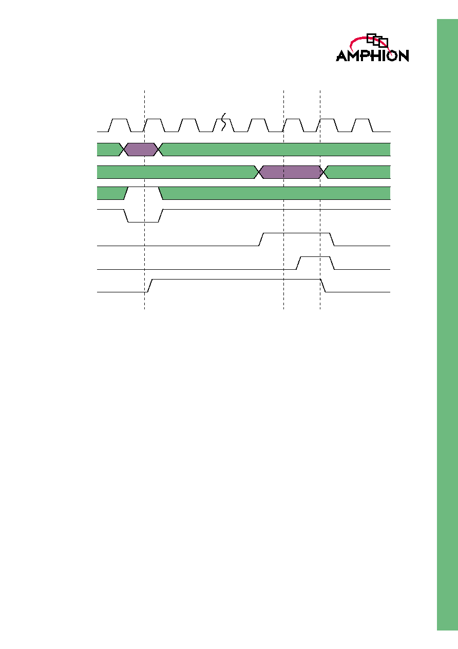
DISPLAY DMA OUTPUT PIXEL INTERFACE
Figure 4: Picture DMA Outputs
In this example, the 4:2:2 sampled pixel set consists of the
luminance (Y) values 5F and 52, the blue chrominance
difference value 3C, and the red chrominance difference value
A7. The bottom two bits of P_DataType are indicating the
sample type currently being output on P_DataOut. The top
two bits indicate that a progressive frame is being output.
This waveform shows P_DataAvail is not asserted for the
clock cycle before the pixel group commences. During this
time the P_DataOut and P_DataType values are undefined
and P_DataStrobe is ignored. Also, the initial clock cycles of
the 3C and 52 values are not accepted by the external logic,
P_DataStrobe is not asserted, so the CS6651 continues to drive
those old values for another clock cycle.
In this example the sample set is the last in the current row, so
P_RowDoneOut is asserted. The diagram also shows how the
external logic can indicate P_RowDoneIn to the core. In this
case the signal has no effect since P_RowDoneOut was
asserted already. Use of P_PicDoneOut and P_PicDoneIn is
similar.
P_General is not shown here and simply reflects the value
currently programmed into the Display DMA Controller's
GeneralDataValue register.
00
00
01
B3
Clk
ES_Data[7:0]
ES_Valid
ES_Stall
5F
3C
52
A7
0000
0010
0001
0011
Clk
P_DataOut[7:0]
P_DataType[3:0]
P_DataAvail
P_DataStrobe
P_RowDoneOut
P_RowDoneIn

7
TM
THE SDRAM INTERFACE
The SDRAM interface timing is completely specified by JEDEC SDRAM standards.
HOST INTERFACE
The host interface is effectively in two parts, a Configuration and Status register read and write section and a Host to memory
read and write access section.
Figure 5: Host Write to Configuration Register and Host Read of Configuration or Status Register
Figure 5 illustrates a host write to a configuration register and
a host read of a configuration or status register. The write
happens on the rising edge of the Clk signal indicated by the
line A. The H_DataOut bus reflects the new value in the
register on the next clock cycle. The read cycle is synchronous.
Whenever H_notRegCS is asserted and the H_notWrite signal
is not, then H_notDatDrv will be asserted in the following
cycle, when H_DataOut is valid. This can be used to enable
tristate drivers on a bi-directional host data bus, if required.
AWrite
Din
ARead
A
Clk
H_Addr [21:0]
H_DataIn [31:0]
H_notRegCS
H_notWrite
H_notDatDrv
H_DataOut [31:0]
Din
Dout

8
CS6651
MPEG-2 Video Decoder for FPGA
Figure 6: Host Writing Location in Memory
In Figure 6, the host is writing a location in memory. On clock
cycle A the write address is latched since H_notMemWrite
was asserted by the host. A single clock cycle of data is made
available to the decoder core on clock cycle B using
H_MemWrValid. On clock cycle C the core loads the data and
performs the write. The data load is indicated by the assertion
of H_MemWrReady.
In this example the bottom two bytes of H_DataIn, i.e. 15:0,
were enabled. Only these two bytes of the memory will be
written. Bits 31:16 of the memory location will remain
unchanged.
The above diagram shows the write spread out over three
clock cycles. Normally, when the memory interface is not busy
and the host has the address and data available together, clock
cycles A, B and C will all be on the same rising edge.
H_MemBusy remains asserted until clock cycle D, when the
memory write actually reaches the memory controller. This
signal can be used to insert wait states into a host interface
controller if necessary.
Clk
H_Addr[21:0]
H_DataIn[31:0]
H_ByteEnable[3:0]
H_notRegCS
H_notMemWrite
H_MemWrValid
H_MemWrReady
H_MemBusy
Write
D
0011
IN
A
B
C
D
A
9
TM
Figure 7: Host Reading Location in Memory
In Figure 7, the host is reading a location in memory. On clock
cycle A the read address is latched due to H_notMemRead
being asserted by the host. On this edge H_MemBusy will be
asserted until the read is completed. A single clock cycle of
data is made available by the decoder core on clock cycle B
using H_MemRdValid. On clock cycle C the external logic
loads the data and completes the read, indicated by the
assertion of H_MemRdStrb. On this clock cycle the core clears
H_MemBusy. The entire word is read from memory and made
available on H_DataOut, regardless of the state of the
H_ByteEnable port.
Clk
H_DataIn[31:0]
H_Addr[21:0]
H_notRegCS
H_notMemRead
H_MemRdValid
H_MemRdStrb
H_MemBusy
A
B
C
A
Read
D
OUT
10
CS6651
MPEG-2 Video Decoder for FPGA
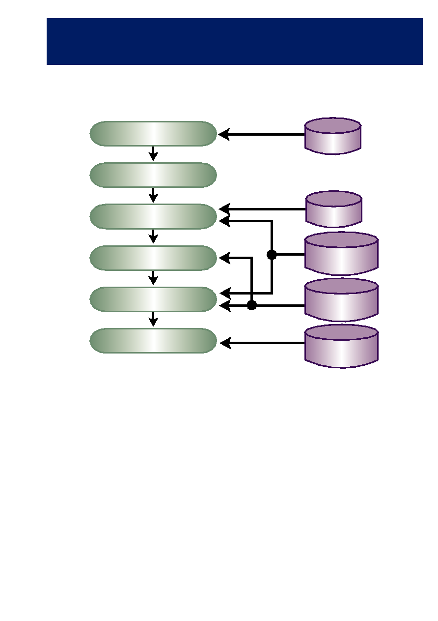
CS6651 DESIGN METHODOLOGY
Figure 8: Design Data Formats Supplied by Amphion
ASVC Data Formats
Supplied by AMPHION
Typical ASIC or FPGA Design Flow
(Conceptual)
Bit Accurate
C Model
RTL Simulation
Models
Testbench
(VHDL & Verilog)
Netlists
(Verilog, VHDL, EDIF, .bd)
FPGA Programming
Files
System-Level "C" Code simulation
Hardware RTL Development
RTL Simulation
Logic Synthesis
Gate-level analysis
(timing & functional)
Physical Design

11
TM
AVAILABILITY AND IMPLEMENTATION INFORMATION
PROGRAMMABLE LOGIC CORES
For ASIC prototyping or for projects requiring the fast time to market of a programmable logic solution, Amphion's
programmable logic core solutions offer the silicon-aware performance tuning found in all Amphion products, combined with
the rapid design times offered by today's leading programmable logic solutions.
Table 7: CS6651 Programmable Logic Cores
PRODUCT
ID#
SILICON
VENDOR
PROGRAMMABLE
LOGIC PRODUCT
DEVICE RESOURCES
USED (LOGIC)
DEVICE RESOURCES
USED (MEMORY)
AVAILABILITY
CS6651AA
Altera
Apex 20KE FPGA
16041 LEs
28 ESB
NOW
CS6651XV
Xilinx
Virtex-E FPGA
7377 Slices
18 Block RAMs
NOW

CS6651
MPEG-2 Video Decode for FPGA
TM
Virtual Components for the Converging World
CORPORATE HEADQUARTERS
Amphion Semiconductor Ltd
50 Malone Road
Belfast BT9 5BS
Northern Ireland, UK
Tel:
+44.28.9050.4000
Fax:
+44.28.9050.4001
EUROPEAN SALES
Amphion Semiconductor Ltd
CBXII, West Wing
382-390 Midsummer Boulevard
Central Milton Keynes
MK9 2RG England, UK
Tel:
+44 1908 847109
Fax:
+44 1908 847580
WORLDWIDE SALES & MARKETING
Amphion Semiconductor, Inc
2001 Gateway Place, Suite 130W
San Jose, CA 95110
Tel:
(408) 441 1248
Fax:
(408) 441 1239
CANADA & EAST COAST US SALES
Amphion Semiconductor, Inc
Montreal
Quebec
Canada
Tel:
(450) 455 5544
Fax:
(450) 455 5543
Web: www.amphion.com
Email: info@amphion.com
� 2001-02 Amphion Semiconductor Ltd. All rights reserved.
Amphion, the Amphion logo,"Virtual Components for the Converging World", are trademarks of Amphion Semiconductor Ltd. All others are the property of their
respective owners.
12
08/02 Publication #: DS6651 v1.3
ABOUT AMPHION
Amphion
(formerly
Integrated
Silicon Systems) is the leading
supplier of speech coding, video/
image
processing
and
channel
coding application specific silicon
cores for system-on-a-chip (SoC)
solutions
in
the
broadband,
wireless, and mulitmedia markets.
SALES AGENTS
SPS-DA PTE LTD
21 Science Park Rd
#03-19 The Aquarius
Singapore Science P ark II
Singapore 117628
T el:
+65 774 9070
Fax:
+65 774 9071
SPINNAKER SYSTEMS INC
Hatchobori SF Bldg. 5F 3-12-8
Hatchobori, Chuo-ku
T oky o 104-0033 Japan
Tel:
+81 3 3551 2275
Fax:
+81 3 3351 2614
V oy ageur T echnical Sales Inc
1 Rue Holiday
T our Est, Suite 501
P oint Claire, Quebec
Canada H9R 5N3
T el:
(905) 672 0361
Fax:
(905) 677 4986
JASONTECH, INC
Hansang Building, Suite 300
Bangyidong 181-3, Songpaku
Seoul Korea 138-050
T el:
+82 2 420 6700
Fax:
+82 2 420 8600
Phoenix T echnologies Ltd
3 Gavish Street
Kfar -Saba, 44424
Israel
T el:
+972 9 7644 800
Fax:
+972 9 7644 801