 | –≠–ª–µ–∫—Ç—Ä–æ–Ω–Ω—ã–π –∫–æ–º–ø–æ–Ω–µ–Ω—Ç: CS6654 | –°–∫–∞—á–∞—Ç—å:  PDF PDF  ZIP ZIP |
TM
Virtual Components for the Converging World
Amphion continues to expand its family of application-specific cores
1
See http://www.amphion.com for a current list of products
CS6652/54
Multi-stream MPEG-2 Video Decoders
The CS6652/CS6654 MPEG-2 multi-stream video decoders provide high performance solutions for applications
requiring simultaneous real-time decoding and display of multiple video streams. The CS6652 and CS6654
provide up to 2 and 4 MPEG-2 MP@ML or 4:2:2P@ML video elementary streams respectively. These high
performance application specific cores can be configured to decode a single video elementary stream up to
MP@HL or 4:2:2P@HL as well as a single ISO/IEC11172-2 (MPEG-1) constrained parameter bitstream. The
CS6652 and CS6654 have been handcrafted by Amphion to deliver high performance while minimizing power
consumption and silicon area for ASICs.
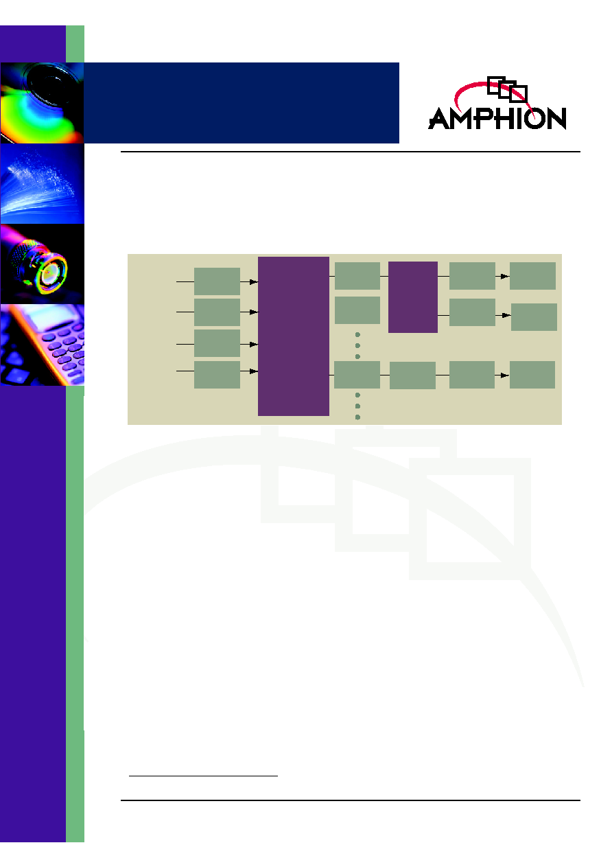
Figure 1: Example Set Top Box Using CS6652 for Simultaneous Display and VCR Recording of Different Programs
Terrestrial
CS6804
Multi-source
Transport
Stream
Demux
Front End
Source0
Front End
Source1
Front End
Source2
Front End
Source3
Storage
Media
Cable
Satellite
Video PES
Parser
Video PES
Parser
CS6652
Multi
Stream
Video
Decoder
Display
(main)
VCR
PAL/NTSC
Encoder
PAL/NTSC
Encoder
Audio PES
Parser
Speaker
Audio
DAC
Audio
Decoder
FEATURES
ISO/IEC 13818-2 (H.262) compliant
-
Supports MP@ML to 4:2:2P@HL
High performance solution for high data rate
MPEG-2 decoding
-
Supports input bit rates up to 300 Mbps
-
Real time decode and display of 2 or 4
streams of up to 4:2:2P@ML or a single
stream of up to 4:2:2P@HL
Supports all ATSC and HDTV defined resolutions
and frame rates
Supports progressive and interlaced scan
Supports intra slice refresh
Bitstream error detection and recovery
Glueless interface to external SDRAM
Capable of standalone or host controlled opera-
tion
Fully Synchronous design with host shutdown
and restart control
Ease of integration
-
Simple core interface for easy integration into
larger systems.
KEY METRICS
1
Logic area:
89.5K Gates
Memory:
11.75K Bits RAM
Maximum clock:
133 MHz
APPLICATIONS
DVB-T, DVB-S or DVB-C set-top-box/integrated
receiver decoders
Digital cable and satellite set-top decoder box
for ATSC HDTV
DVD Video - Standard and High Definition
Studio 4:2:2 chrominance format editing or
production
Picture-in-picture or simultaneous viewing of 2,
3, or 4 channels
PC video hardware acceleration
Simultaneous display or recording of 2 or more
channels
BENEFITS
Highly parallel architecture provides cost effi-
cient approach for compute intensive video
decoding
Simplifies system architecture to reduce overall
HW/SW coverification period
Low power to help minimize packaging cost
1. This information is for CS6652-Lite core which is a reduced gate count version not including the SDRAM memory controller and display DMA. For more
information please refer to Table 3 & 4.
2
CS6652/54
Multi-stream MPEG-2 Video Decoders
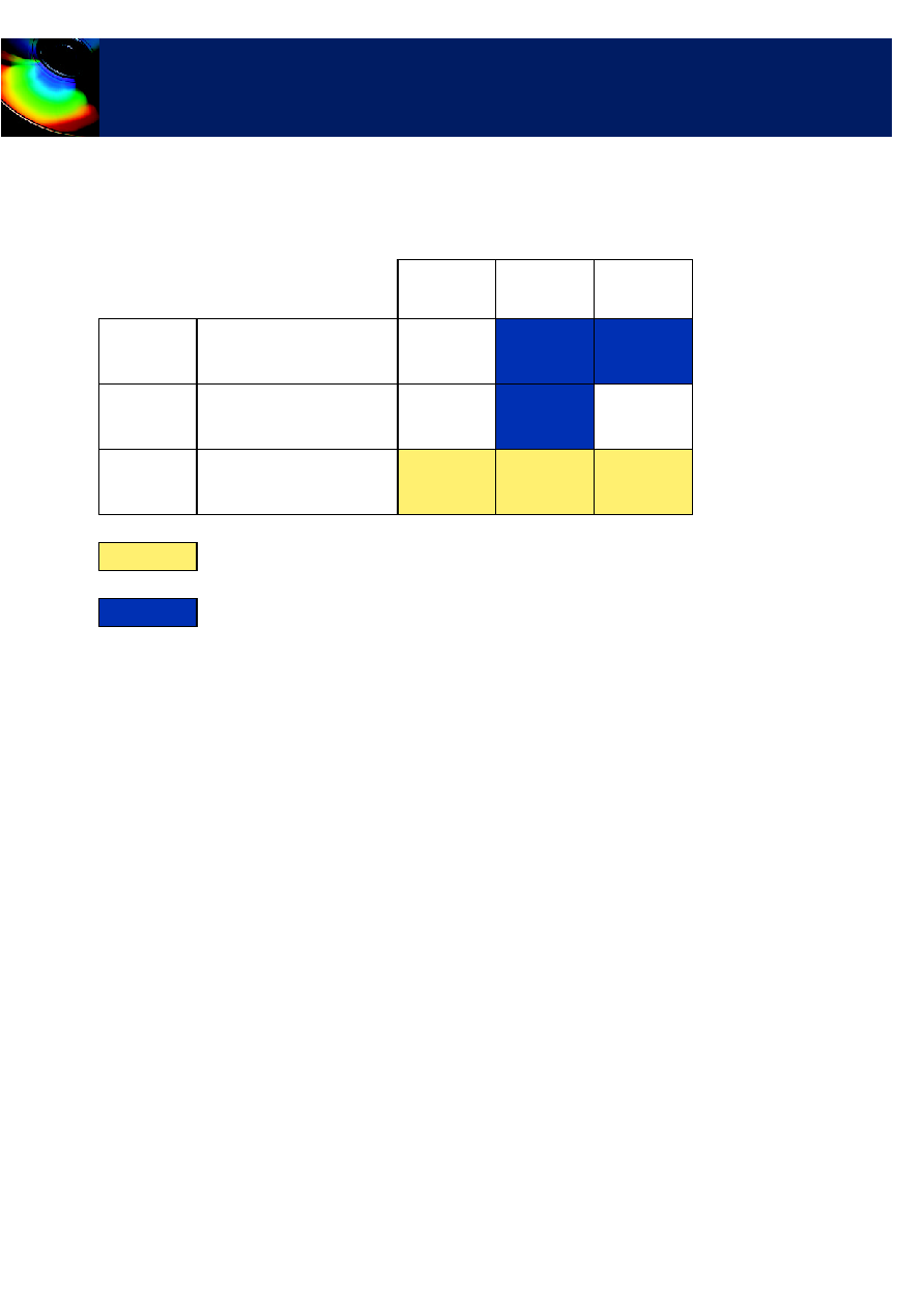
CS6652/CS6654 MPEG-2 MULTISTREAM VIDEO DECODERS
Table 1 Defines MPEG-2 profiles and levels supported by the CS6652 & CS6654 MPEG-2 multistream video decoders.
The CS6652/CS6654 cores accept video elementary streams as
input from conditional access decryption, transport stream
demux, or similar sources. These streams are input on a byte-
wide port with handshake flow control signals, allowing a
maximum overall average input bitrate of 300Mbits/sec. The
cores can operate in a default mode on input streams without
the intervention of a host processor. In this mode pictures will
be decoded from the video streams and output in correct
display order. The host processor has access to a full range of
information for each input stream and can control the
behavior of the decoder to permit audio/video
synchronization, pan-scan, letterbox conversion, and various
trick modes. The output from the cores is provided by highly
configurable display DMA (Direct Memory Access) engine.
This allows adjustable output video component sequencing
for each input stream and provides external logic with control
over the display of the picture. To meet the high bandwidth
requirements of the simultaneous decoding and display of up
to four 4:2:2P@ML elementary streams (or a single 4:2:2P@HL
elementary stream), a bank of two SDRAM chips is used.
These SDRAM chips are commodity 64Mbit PC133 SDRAMs
in 2Mx32 configuration.
Table 1: MPEG-2 Profiles and Levels Supported by CS6652/54 Cores
Level
Profile
Simple
Main
4:2:2
High
Samples/line
Lines/frame
Frames/sec
Max. luma samples rate
1920x
1088x
60
62668800
1920x
1088x
60
62668800
High 1440
Samples/line
Lines/frame
Frames/sec
Max. luma samples rate
1440x
1088x
60
47001600
Main
Samples/line
Lines/frame
Frames/sec
Max. luma samples rate
720x
576x
30
10368000
720x
576x
30
10368000
720x
608x
30
11059200
Multistream Mode
Single stream Mode
3
TM
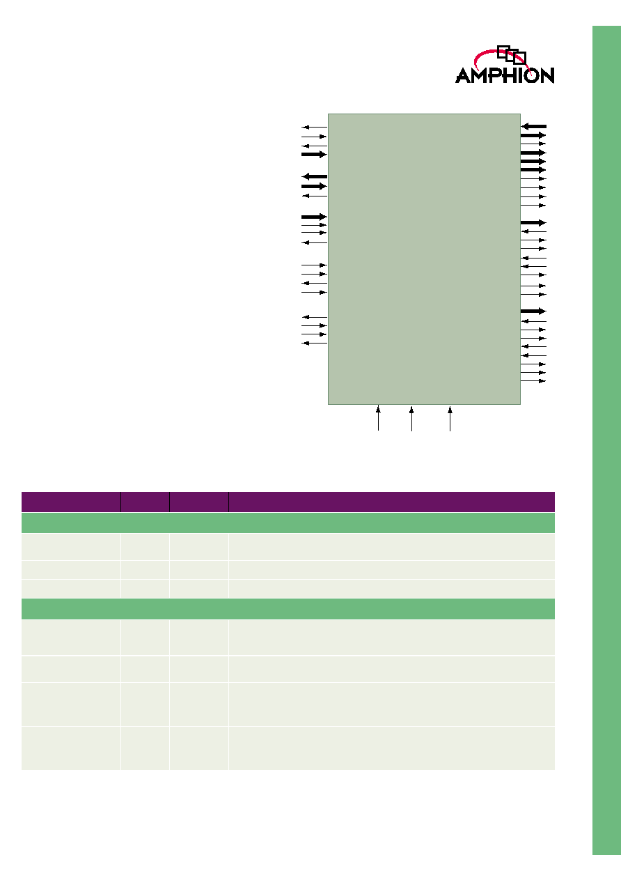
CS6652/CS6654 SYMBOL AND PIN
DESCRIPTION
Table 2 gives the descriptions of the input and output ports
(shown graphically in Figure 2) of the CS6652 MPEG-2
multistream video decoder. Unless otherwise stated, all
signals are active high and bit(0) is the least significant bit.
Figure 2: CS6652 Symbol
ES_Select
ES_Valid
ES_Stall
ES_Data[7:0]
H_DataIn[31:0]
H_DataOut[31:0]
H_notDatDrv
H_Addr[21:0]
H_notRegCS
H_notWrite
H_notIRQ
H_notMemRead
H_notMemWrite
H_MemBusy
H_ByteEnable[3:0]
H_MemRdValid
H_MemRdStrb
H_MemWrValid
H_MemWrReady
SD_DataIn[63:0]
SD_DataOut[63:0]
SD_notDatDrv
SD_Addr[10:0]
SD_BA[1:0]
SD_DQM[7:0]
SD_notRAS
SD_notCAS
SD_notWE
SD_notCS
P_Data_0[15:0]
P_DataStrobe_0
P_Data_Avail_0
P_DataType_0[3:0]
P_RowDoneIn_0
P_PicDoneIn_0
P_RowDoneOut_0
P_PicDoneOut_0
P_General_0[7:0]
P_Data_1[15:0]
P_DataStrobe_1
P_DataAvail_1
P_DataType_1[3:0]
P_RowDoneIn_1
P_PicDoneIn_1
P_RowDoneOut_1
P_PicDoneOut_1
P_General_1[7:0]
CS6652
Clk notReset CoreReset
Table 2: CS6652/54 Interface Signal Definitions
Signal
Width
I/O
Description
Global Signals
Clk
1
Input
Core clock Master clock used for all logic and the external SDRAM interface. This clock
should also be routed to the external SDRAM chips. The clock is 133MHz
notReset
1
Input
Core reset Asynchronous, active low global core reset.
CoreReset
1
Input
Core reset Synchronous, active high core reset.
Elementary Stream Input Interface
ES_Data
8
Input
Elementary Stream Data, byte aligned video elementary stream bytes from the Condi-
tional Access decryption core or transport stream demux. Maximum average input bit
rate is 300Mbits/s
ES_Valid
1
Input
Data Valid Strobe, ES_Data is latched on the positive edge of Clk when ES_Valid is
asserted and ES_Stall is not asserted.
ES_Stall
1
Output
Data Stall, input data may be burst into the core at a rate higher than the specified max-
imum 300Mbits/s. In this case the core will indicate that it temporarily cannot receive
any more data by assertion of ES_Stall. ES_Data and ES_Valid will be ignored while
ES_Stall is asserted.
ES_Select
1 or 2
Output
Elementary Stream Select, either a 1-bit (CS6652) or 2-bit (CS6654) signal represent-
ing the number of the elementary stream which the core is currently accepting and
decoding via ES_Data. This signal may be used to drive a mux to switch the correct
elementary stream into the core when selected.

4
CS6652/54
Multi-stream MPEG-2 Video Decoders
Picture Output Interface (One per elementary stream)
P_Data
16
Output
Picture Output Data, from the display DMA. Contains either Y, Cr or Cb, as indicated by
P_DataType. In 16-bit mode the upper 8 bits carry Y and the lower 8 bits carry either Cr
or Cb as indicated by P_DataType.
P_DataStrobe
1
Input
Data Taken Strobe, indicates that the external logic will consume the current P_Data on
the next positive edge of Clk. The signal is also used as a qualifier for the
P_RowDoneIn and P_PicDoneIn signals.
P_DataAvail
1
Output
Data Valid Signal, indicates that the DMA engine has been configured and is running
and P_Data carries a valid picture sample.
P_DataType
4
Output
Picture Data Type, indicates the type of sample on P_Data. The bottom two bits carry
the component identification as follows:
00 = Y
1
01 = Y
2
10 = Cb
11 = Cr.
The top two bits carry display frame/field information as follows:
00 = progressive
01 = undefined
10 = top field
11 = bottom field.
P_RowDoneIn
1
Input
Last Pixel in Row, used to terminate a row scan and move on to the next. This may be
used with pan and scale external logic. This input is ignored in certain DMA configura-
tions. Should be asserted for the last byte of the pixel sample group ≠ the engine will
stop after the last component for the group is taken.
P_PicDoneIn
1
Input
Last Pixel in Picture, indicates that the display of the picture is complete at the end of
the current pixel. The engine will revert to idle mode. This input is ignored in certain
DMA configurations. Should be asserted for the last byte of the pixel sample group ≠
the engine will stop after the last component for the group is taken.
P_RowDoneOut
1
Output
Last Pixel in Row, This output can be programmed to indicate the last component of the
last pixel of the row. This requires the correct configuration of the DMA engine row
length register.
P_PicDoneOut
1
Output
Last Pixel in Picture, This output can be programmed to indicate the last component of
the last pixel of the picture. This requires the correct configuration of the DMA engine
row and column length registers.
P_General
8
Output
General Outputs, These outputs directly reflect the programmed value in the DMA gen-
eral Output register. They can be used by the host CPU to inform the display logic of
specific display parameters such as PAL/NTSC encoding information etc.
Frame Store Interface
SD_DataIn
64
Input
SDRAM Data Input, read data input from external SDRAM.
SD_DataOut
64
Output
SDRAM Data Output, write data output to external SDRAM.
SD_notDatDrv
1
Output
SDRAM Data Drive, active LOW enable signal for SDRAM data bus tristate drivers.
Driven low when SD_DataOut should be placed on the bus.
SD_Addr
11
Output
SDRAM Address bus, carries row or column addresses or commands to the external
SDRAM.
SD_BA
2
Output
SD_BA, indicates selected bank for the current SDRAM command.
SD_DQM
8
Output
SDRAM DQ Mode, used to control burst transfers of data to/from the SDRAM.
SD_notRAS
1
Output
SDRAM Row Address Strobe, strobes a row address or command into the SDRAM.
SD_notCAS
1
Output
SDRAM Column Address Strobe, strobes a column address or command into the
SDRAM.
SD_notWE
1
Output
SDRAM Write Enable, indicates to the SDRAM that a write command is required.
SD_notCS
1
Output
SDRAM Chip Select, active except for reset.
Table 2: CS6652/54 Interface Signal Definitions
Signal
Width
I/O
Description

5
TM
Host Interface
H_DataIn
32
Input
Host Data Input, host write data into the core.
H_DataOut
32
Output
Host Data Output, host read data from the core. This pipelined output reflects the value
of the register selected by H_Addr.
H_notDatDrv
1
Output
Host Data Drive, indicates that a read is active. This can be used to control external
tristate drivers if required. Active LOW.
H_Addr
22
Input
Host Address, used to select a register for read/write, or a frame store SDRAM word to
be accessed.
H_notRegCS
1
Input
Host Chip Select, active LOW enable signal controls all host register accesses.
H_notWrite
1
Input
Host Write Select, indicates that when H_notRegCS is asserted, the register addressed
by H_Addr will have the value on H_DataIn assigned to it on the rising edge of the Clk
signal, if the appropriate byte write enable signal is also asserted. If it is de-asserted
when H_notRegCS is asserted then a register read is initiated and H_DataOut will
show the selected register's data on the next tick.
H_notIRQ
1
Output
Host Interrupt Request, active LOW output asserted when an interrupt condition is
present and enabled.
H_ByteEnable
4
Input
Host Byte Write Enables, used on write accesses to control which bytes in a register or
SDRAM word actually get written.
H_notMemRead
1
Input
Host memory Read Access, initiates an SDRAM host read transaction.
H_notMemWrite
1
Input
Host Memory Write Access, initiates an SDRAM host write transaction.
H_MemBusy
1
Output
Host Memory Interface Busy, indicates that a memory access transaction is in
progress. This can be used to insert read wait states and to stall for posted writes to
complete.
H_MemRdValid
1
Output
Host Memory Read Data Valid, indicates that the read data is available on the
H_DataOut port.
H_MemRdStrb
1
Input
Host Memory Read Data Strobe, indicates that the host will consume the data from the
H_DataOut port on the next positive edge of Clk.
H_MemWrValid
1
Input
Host Memory Write Data Valid, indicates that the host has placed valid write data on the
H_DataIn port. Note that H_ByteEnable should be valid at the same time as the data.
H_MemWrReady
1
Output
Host Memory Write Data Ready, indicates that the core is ready to consume the data
on H_DataIn on the positive edge of Clk when it is signalled as valid with
H_MemWrValid.
Table 2: CS6652/54 Interface Signal Definitions
Signal
Width
I/O
Description
6
CS6652/54
Multi-stream MPEG-2 Video Decoders
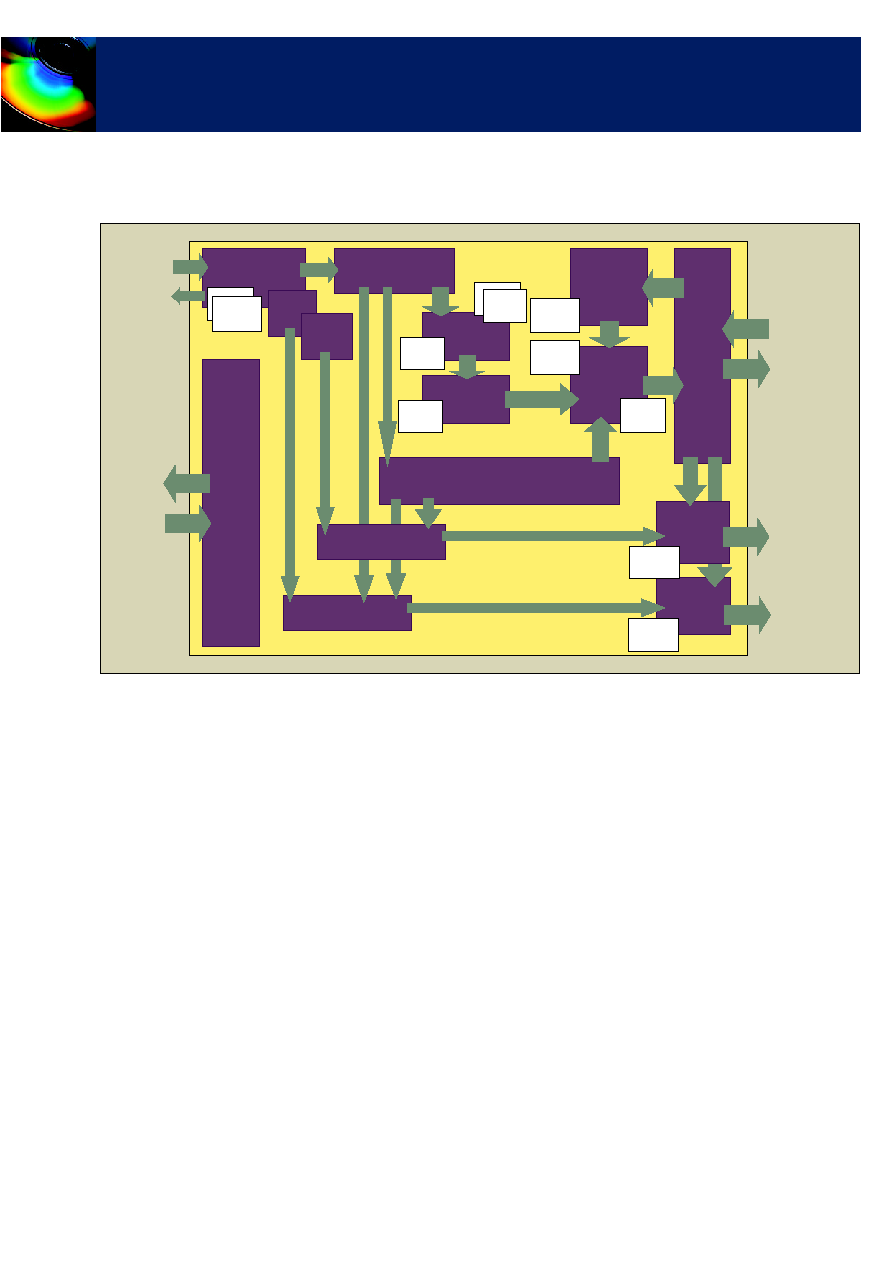
CS6652/CS6654 FUNCTIONAL DESCRIPTION
Figure 3 represents a block diagram of the main functional blocks in the CS6652. This is followed by a high-level description of
these blocks, which is equally applicable to the CS6654.
Figure 3: CS6652 Multi-stream MPEG-2 Video Decoder Block Diagram Showing Memory Blocks
STREAMSELECT: ELEMENTARY
STREAM SWITCHING AND SELECTION
This controls switching between input elementary streams
and the selection of the correct parameters for a particular
stream, when the decoding of that stream is in progress. In
multi-stream mode switching from decoding one elementary
stream to another is done at the slice layer, specifically at the
end of a macroblock row. In MPEG-2 video the start and end
of a row of macroblocks always corresponds with the start
and end of a slice, although a macroblock row may contain
more than one slice. Within a slice various macroblock data is
coded differentially between the macroblocks (e.g. DC DCT
coefficient, motion vectors). This means that the slice provides
a carefully encapsulated group of data, at the end of which
switching from one stream to another can be done with a
minimal requirement to store state, base and incremental
values of macroblock parameters.
Switching from decoding one stream to another is only done
when the last slice of the macroblock row has been decoded.
Therefore, each elementary stream is decoded one macroblock
row at a time, rather than simply slice by slice. This prevents
streams with a longer slice structure from monopolizing the
decoder. Switching at the slice layer necessitates the storage of
state variables in both the Video Stream Parser and VLC
Decoder, as well as the replication of various input buffers
and FIFOs for each elementary stream.
ES Parser
VLC Decoder
RLD &
Iquant
Inverse DCT
Motion
Comp
Pixel
Recon
Frame
Store
Interface
Host
Interface
Regs
0
Frame
Store
SDRAMs
Stream Control 0
Output
Picture Data
(stream 0)
Input
Video ES
CS
mem
TRN
mem
IDCT
mem
PB
mem
PWB
mem
DB
mem
ES Select
Regs
1
Control & Stream Select
Display
DMA1
DB
mem
Stream Control 1
Host
micro-
processor
Display
DMA0
ASD
mem
Output
Picture Data
(stream 1)
ASD
mem
QM
mem
QM
mem
ASD mem
CS mem
QM mem
TRN mem
PB mem
IDCT mem
PWB mem
DB mem
- Additional Stream Data memories
- Convert Scan memory
- Quantization matrix memories
- IDCT matrix memories
- Prediction Buffer memory
- IDCT coefficient memory
- Pixel Write-back memory
- Display Line-Buffer memory

7
TM
STREAMDECODE: FROM STREAM
DECODING TO INVERSE DCT
Elementary Stream Interface
This interface accepts elementary stream data through the
byte wide ES_Data port. If the core temporarily cannot receive
any further data, or is switching from one elementary stream
to another ES_Stall is asserted. In the CS6652 or CS6654 the
ES_Select output is either a single or 2-bit signal, respectively,
representing the number of the elementary stream that the
core is currently accepting and decoding via ES_Data. This
signal may be used to drive a multiplexer to switch the correct
elementary stream into the core when selected.
Video Stream Parser
VLC Decoder
The VLC Decoder block decodes the Huffman-style variable
length encoded picture data. At the macroblock layer the
outputs of VLC Decoder include:
∑
DCT block run-level information
∑
Decoded motion vectors for motion compensation
∑
A number of information fields describing the section of
the picture currently being decoded.
The registers used to store stream parameters are replicated as
necessary for each multistream pipeline in the core.
Run-Level Decoding and Inverse Quantization
The output run-level information from the VLC decoder is
converted into complete blocks of 64 quantized DCT
coefficients by the Run-Level Decoder. These DCT coefficients
are encoded in Zigzag or Alternate Scan order and are
converted to natural row order using the Convert Scan (CS)
memory before dequantization. Custom quantization
matrices can be used in the encoding of MPEG video. These
are sent as part of the header information in the stream and
are stored in the Quantization Matrix (QM) memory. The
dequantized DCT blocks are then passed to the Inverse DCT
unit.
Inverse DCT
This high performance unit performs the inverse transform of
the 8x8 DCT Y, Cr and Cb sample blocks. It is capable of
streaming data through continuously transforming an entire
block of 8x8 DCT coefficients into an 8x8 block of (IDCT)
samples or sample prediction error corrections in every 64
clock cycles.
PICRECON: MOTION COMPENSATION
AND PICTURE RECONSTRUCTION
Motion Compensation Unit
For each macroblock in a P- or B-picture the motion
compensation unit takes the decoded motion vectors from the
VLC Decoder and translates them into row and column co-
ordinates for the prediction samples in the reference picture.
The pixels at those co-ordinates are then requested from the
Memory System frame store interface. When the requested
samples are received they are combined with other (forward/
backward/dual prime) samples for the same block to complete
the prediction for the macroblock.
Picture Reconstruction
In this block the final motion compensation prediction
samples are merged with the sample prediction error
corrections from the Inverse DCT unit to form the final
reconstructed samples for the macroblock. They are then
stored in the pixel write-back buffer before being written to
the frame store. In the case of intra macroblocks there are no
prediction samples to add and the output IDCT samples are
written back to the frame store without any further
processing.
STREAMCONTROL: FRAME BUFFER
TRACKING AND DISPLAY CONTROL
There is one StreamControl block for each input elementary
stream. This block is responsible for controlling the decoding
process, reordering, and queuing of pictures for display, for its
designated elementary stream. This task involves the tracking
of the contents of the frame store. For multistream operation
the SDRAM is divided into 2 or 4 separate frame stores in the
CS6652 and CS6654, respectively. The StreamControl block
keeps track of frame buffers and off loads them for reuse once
the frames they contain are no longer required for either
reference or display.
MEMSYS: SDRAM FRAME STORE
INTERFACE
The Frame Store is implemented using two SDRAM chips,
which are commodity PC133 64Mbit parts, each with 2Mx32
organization. The memory interface runs at 133 MHz and can
be directly connected to the SDRAM chips using suitable
pads. MemSys handles the mapping of pixel read and write
requests for motion compensation, reconstructed pixel write-
back, and display into linear memory addresses. Additionally,
the host interface can access the memory banks. Arbitration
between the various accessing units and memory transaction
queues are all maintained by this module.

8
CS6652/54
Multi-stream MPEG-2 Video Decoders
DMA: PICTURE DISPLAY DMA (ONE
PER ELEMENTARY STREAM)
The picture display DMA has a double-byte output interface
that can carry Y, Cr or Cb pixel data. Y and Cr or Cb data can
be output simultaneously as 16-bit wide composite values or
sequentially as four separate bytes. For 4:2:0 chrominance
format video streams the Picture Display DMA will upsample
the chrominance vertically to provide a 4:2:2 output. The
Display DMA engine can be configured by the host CPU via
the Host Interface to display only a particular portion of the
decoded picture, or in stand-alone mode, the entire coded
picture. A number of handshake signals are provided on the
Picture Display DMA interface. These signals allow external
logic to control the timing of the pixel output stream and
control the end of the current scan row or picture display.
Outputs indicate the nature of the pixel being currently driven
to the external logic. Also, end of row and end of picture flags
allow the sync pulse generation.
HOSTINTERFACE: CONFIGURATION
AND CONTROL
When the CS6652 or CS6654 is running with the assistance of a
host CPU, a number of additional features can be accessed. All
of the interfacing between the host and the CS6652 or CS6654
is performed through the HostInterface. This allows the read/
write access to all the internal control, status and video stream
parameter registers (for each stream) within the decoder. The
HostInterface also provides a simple 32-bit read/write access
to the SDRAM Frame Store. Normally, the areas of the
SDRAM used for storage of picture data cannot be accessed
by the HostInterface; however, a bypass mode allowing direct
access is provided for system diagnostic tests etc. An interrupt
request is also included on the HostInterface.
9
TM
AVAILABILITY AND IMPLEMENTATION INFORMATION
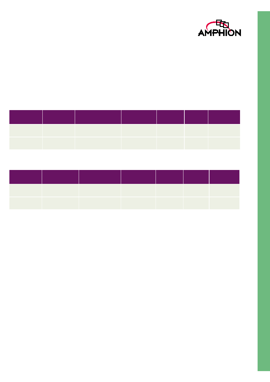
ASIC CORES
For applications that require the high performance, low cost and high integration of an ASIC, Amphion delivers application
specific silicon cores that are pre-optimized to a targeted silicon technology by Amphion experts.
Consult your local Amphion representative for product specific performance information, current availability of individual
products, and lead times on ASIC core porting.
* Logic gates do not include clock circuitry
** Reduced address mapped register set. Does not include SDRAM memory controller or display DMA
Table 3: CS6652 Core Using TSMC Standard Cell Libraries
Product ID #
Process
Technology
Supported Profile
and Level
Clock Speed
(MHz)
Logic*
Gates
Memory
(RAM)
Availability
CS6652TM Lite**
130 nm
2x MP@ML
1x MP@HL
133
9.75K
9.75KBits
Now
CS6652TM
130 nm
2x 4:2:2P@ML
1x 4:2:2P@HL
133
111.5K
19.75KBits
Now
Table 4: CS6654 Core Using TSMC Standard Cell Libraries
Product ID #
Process
Technology
Supported Profile
and Level
Clock Speed
(MHz)
Logic*
Gates
Memory
(RAM)
Availability
CS6654TM Lite**
130 nm
4x MP@ML
1x MP@HL
133
106K
11.75KBits
Now
CS6654TM
130 nm
4x 4:2:2P@ML
1x 4:2:2P@HL
133
127K
31.75KBits
Now

CS6652/54
Multi-stream MPEG-2 Video Decoders
TM
Virtual Components for the Converging World
CORPORATE HEADQUARTERS
Amphion Semiconductor Ltd
50 Malone Road
Belfast BT9 5BS
Northern Ireland, UK
Tel:
+44 28 9050 4000
Fax:
+44 28 9050 4001
EUROPEAN SALES
Amphion Semiconductor Ltd
CBXII, West Wing
382-390 Midsummer Boulevard
Central Milton Keynes
MK9 2RG England, UK
Tel:
+44 1908 847109
Fax:
+44 1908 847580
WORLDWIDE SALES & MARKETING
Amphion Semiconductor, Inc
2001 Gateway Place, Suite 130W
San Jose, CA 95110
Tel:
(408) 441 1248
Fax:
(408) 441 1239
CANADA & EAST COAST US SALES
Amphion Semiconductor, Inc
Montreal
Quebec
Canada
Tel:
(450) 455 5544
Fax: (450)
455
5543
Web:
www.amphion.com
Email: info@amphion.com
Phoenix Technologies Ltd
3 Gavish Street
Kfar-Saba, 44424
Israel
Tel:
+972 9 7644 800
Fax:
+972 9 7644 801
Voyageur Technical Sales Inc
1 Rue Holiday
Tour Est, Suite 501
Point Claire, Quebec
Canada H9R 5N3
Tel:
(514) 693 5009
Fax:
(514) 693 5007
JASONTECH, INC
Hansang Building, Suite 300
Bangyidong 181-3, Songpaku
Seoul Korea 138-050
Tel:
+82 2 420 6700
Fax:
+82 2 420 8600
SPINNAKER SYSTEMS INC
Hatchobori SF Bldg. 5F 3-12-8
Hatchobori, Chuo-ku
Tokyo 104-0033 Japan
Tel:
+81 3 3551 2275
Fax:
+81 3 3351 2614
SPS-DA PTE LTD
21 Science Park Rd
#03-19 The Aquarius
Singapore Science Park II
Singapore 117628
Tel:
+65 774 9070
Fax:
+65 774 9071
© 2002 Amphion Semiconductor Ltd. All rights reserved.
Amphion, the Amphion logo,"Virtual Components for the Converging World", are trademarks of Amphion Semiconductor Ltd. All others are the property of their
respective owners.
10
03/02 Publication #: DS6652/54 v1.0
ABOUT AMPHION
Amphion (formerly Integrated
Silicon Systems) is the leading
supplier of speech coding, video/
image processing and channel coding
application specific silicon cores for
system-on-a-chip (SoC) solutions in
the broadband, wireless, and
mulitmedia markets
SALES AGENTS