 | –≠–ª–µ–∫—Ç—Ä–æ–Ω–Ω—ã–π –∫–æ–º–ø–æ–Ω–µ–Ω—Ç: CS6710TK | –°–∫–∞—á–∞—Ç—å:  PDF PDF  ZIP ZIP |

TM
Virtual Components for the Converging World
Amphion continues to expand its family of application-specific cores
1
See http://www.amphion.com for a current list of products
CS6710
Motion Estimation Controller Accelerator
The CS6710 is the key motion estimation and motion compensation block of both the MPEG-4 encoder and codec
functions. The motion compensation functionality is incorporated to complete the encoder's reconstruction path.
Further to reconstruction of pixels to the reference frame store, the motion compensation unit can be enhanced to
provide full motion compensation for a complete decode functionality as required by a Codec. Figure 1 shows
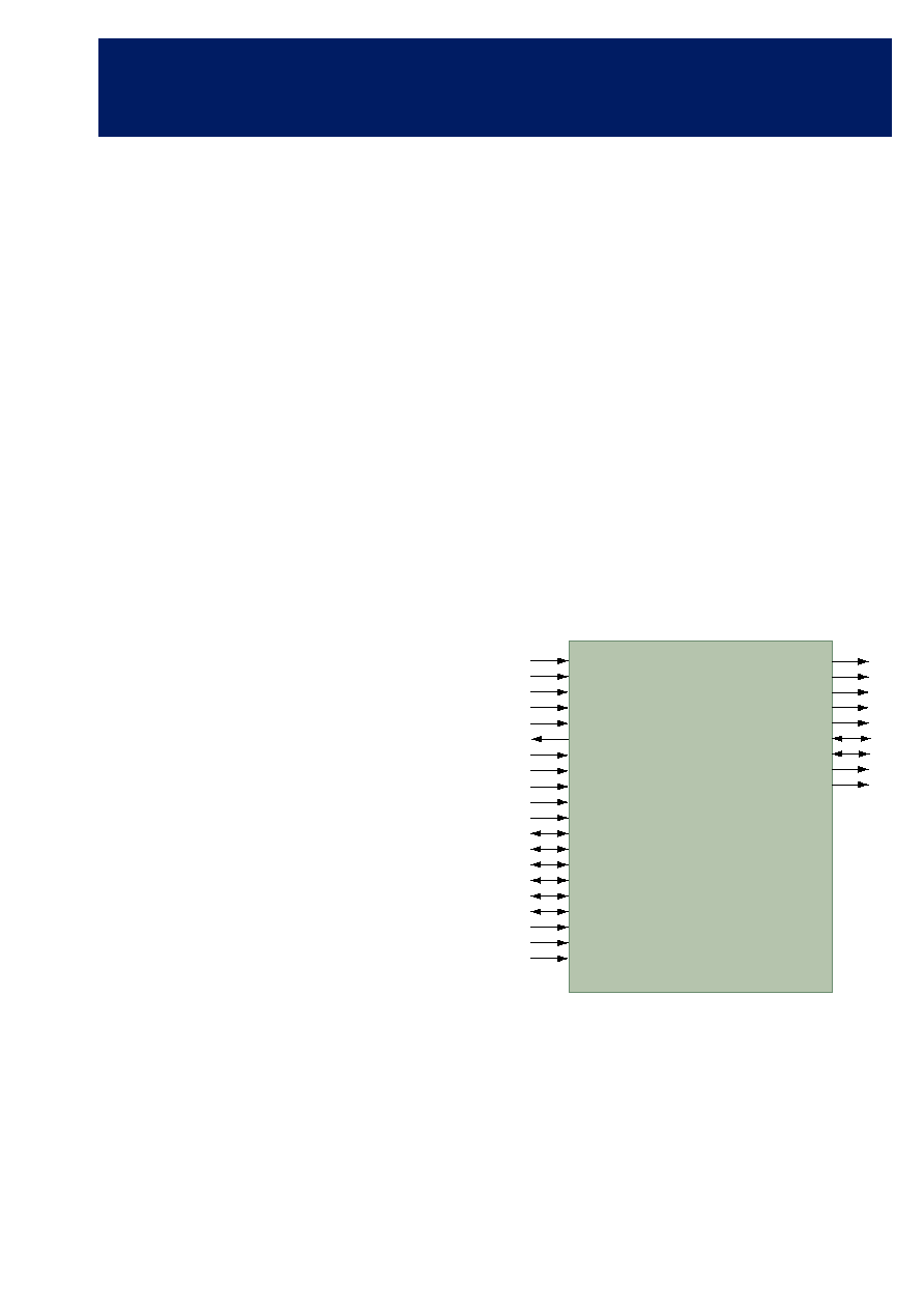
the main functional blocks and interfaces for the CS6710 Motion Estimation Controller accelerator.
Figure 1: CS6710 Motion Estimation Accelerator Block Diagram
Search
Window
Source
MacroBlock
MEControl
SADControl
Pixel
Compression
Interface
Pixel
Compression
Block
Memory Control
Motion
Compensator
AMBA Host Interface
Pre-Processing
Engine
Frame Memory
Search
Algorithm
memory
Reference
MacroBlock
Memory
SADCalc
Pre-Processing
Engine
FEATURES
Programmable Fast Search Algorithm:
-
A micro-sequencer executes with compact
control instructions
-
Instructions based on 'performing the Block
Matching Algorithm at a specified address in
the search window'
-
Base case algorithm is the Cross Search
-
Other options include 3 Step Search and user
defined
-
RAM or ROM based instruction store
SAD Block Matching Algorithm
+/- 16 Search window (expandable)
Unrestricted motion vectors
Integer and 1/2 pixel accuracy
16x16 Motion Vector or 4 8x8 Motion Vectors
Activity Value for each macroblock
Motion Vector Absolute Differences produced
for Luminance and Chrominance components of
the matched block
AMBA AHB compliant; both for Memory and
Register Control accesses
Motion compensation and pixel reconstruction
back path
Memory interface controller for AHB
BENEFITS
Enables maximum design flexibility require-
ments
Relieves the processor of compute intensive
Motion Estimation operation
Motion compensation and Pixel reconstruction
back-path
Reduces overall power consumption
Reduces overall memory and area requirements
2
CS6710
Motion Estimation Controller Accelerator
KEY METRICS
Logic area:
50K Gates
Memory:
29056 bits
Input clock:
100 MHz
APPLICATIONS
Used in MPEG-4 systems such as:
PDAs
PVRs (Personal Video Recorders)
IP cameras
Surveillance & monitoring
Automotive
ARCHITECTURE OVERVIEW
The primary goal of Motion Estimation block is to search a reference VOP frame against a current macroblock for the best motion
estimation. The best motion is estimated through comparing Sum of Absolute differences between a reference frame position and
the current block (16x16 or 8x8 pixels). Once a best match is found a difference block of pixels is provided for all 4 luminance and
the 2 chrominance blocks. Along with this, motion vectors are provided for either the full macroblock or the individual
luminance blocks. Chrominance motion is calculated from the Luminance motion in MPEG-4.
Internally the component comprises a MEControl block that co-ordinates the overall functions of the CS6710 and also initialises
the search window. The SADControl block co-ordinates the SAD and Differences calculations. Within this, the SADCalc block
performs the SAD, Differences and Activity calculations. The Pixel Compression Interface contains the Pixel Compression Input
memory and facilitates access by the Pixel Compression block. The MotionCompensator block performs motion compensation
and the pixel write-back. All accesses to the frame stores are via the Memory Controller. The Source Macroblock RAM can be
filled either through a DMA type access (either by the CS6710 or an external bus master) or through a direct port mapping from a
hardware pre-processing engine.
CS6710 SYMBOL
AND PIN DESCRIPTION
Table 1 describes the input and output ports (shown
graphically in Figure 2) of the CS6710 Motion Estimation
Controller Accelerator. Unless otherwise stated, all signals are
active high and bit(0) is the least significant bit.
The standard interface to this module is AMBA AHB bus
specification. The motion estimation controller requires bus-
mastering capability to the Frame memory but it must also
support slaves accesses from the processor.
Figure 2: CS6710 Symbol
PP_SrcWriteEn
PP_SrcBlkIn
PC_MeAddr
PC_McPixData
HREADY_IN
HREADY_OUT
PC_McCBP
PC_McCBPValid
PC_McBlkAvail
HCLK
HRESETn
HADDR
HTRANS
HWRITE
HSIZE
HBURST
HWDATA
HGRANTx
HMASTER
HMASTLOCK
Gen_Interrup
PC_MePixOut
PC_McPixAddr
PC_McPixRE
PC_McAddrMode
HRDATA
HRESP
HBURSREQx
HLOCK
CS6710
Motion
Estimation
Accelerator

3
TM
Table 1: CS6710 Input and Output Descriptions
Signal
Width
(Bits)
I/O
Description
Extra System Signals
Gen_Interrupt
1
Output
General Interrupt
Active high pulse signal to indicate the following condition
∑
Operation Complete
Pre-processor Port Interface
PP_SrcBlkIn
32
Input
Source MacroBlock
Source pixels from the pre-processor when driven through the port interface
PP_SrcWriteEn
1
Input
Source Write Enable
Write enable signal for the source memory
Pixel Compression Forward Interface
PC_MePixOut
72
Output
ME Pixels Out
Pixels from the PixComp Memory within the MEC.
PC_MeAddr
6
Input
ME Pixel Address
The address of the word in the PixComp Memory to be accessed by the Pixel Compression
unit.
PC_MeRE
1
Input
ME Pixel Read Enable
Asserted to signal that the Pixel data will be consumed on the next rising edge.
Pixel Compensation Return Interface
PC_McPixData
36
Input
Motion Compensation Pixels
The pixels from the Pixel Compression unit that are to be written back to the frame store.
PC_McCBP
6
Input
Coded Block Pattern
Identifies the coded blocks within the macro block.
PC_McCBPValid
1
Input
CBP Valid
Asserted when CBP is valid
PC_McBlkAvail
2
Input
Block Available
Indicates that the pixels on PC_PixIn are valid.
PC_McPixAddr
5
Output
MC Pixels Address
The address of the Pixel Compression pixels.
PC_McPixRE
1
Output
MC Pixel Read Enable
Asserted to signal that the pixels will be consumed on the next rising edge.
PC_McAddrMode
2
Output
Chrominance Address Mode
Indicates that chrominance addressing is being used and identifies the buffer in the Pixel Com-
pression unit that is to be accessed.
AMBA AHB Bus Slave
HCLK
1
Input
Clock Source
All signals related to rising edge of clock
HRESETn
1
Input
Reset Controller
The reset signal is active LOW and is used to reset the system and the bus. This is the only
active LOW signal.
HADDR
32
Input
Address bus
Full address range
HTRANS
2
Input
Transfer type
Indicates the type of the current transfer, which can be NONSEQUENTIAL, SEQUENTIAL,
IDLE or BUSY.
HWRITE
1
Input
Transfer direction
When HIGH this signal indicates a write transfer and when LOW a read transfer.
HSIZE
3
Input
Transfer size
Indicates the size of the transfer, which is typically byte (8-bit), half-word (16-bit) or word (32-
bit).

4
CS6710
Motion Estimation Controller Accelerator
HBURST
3
Input
Burst type
The MEC can support Burst reads/writes. Thus this signal indicates if the burst is Four, eight or
sixteen beat bursts and if the burst is incrementing or wrapping
HWDATA
32
Input
Write Data Bus
32-bit data bus from the processor master or other suitable controlling masters to write in.
HREADY_IN
1
Input
Transfer Done
When HIGH the HREADY_IN signal indicates that a transfer has finished on the bus. This sig-
nal can be driven LOW to extend a transfer.
HREADY_OUT
1
Output
Transfer Done
When HIGH the HREADY_OUT signal indicates that a transfer has finished on the bus. This
signal can be driven LOW to extend a transfer.
HRESP
2
Output
Transfer response
The transfer response provides additional information on the status of a transfer. Four different
responses are provided, OKAY and ERROR.
HRDATA
32
Output
Read Data Bus
32-bit data bus from the MEC on a read request from an external master
AMBA AHB Bus Master
HCLK
1
Input
Clock Source
All signals related to rising edge of clock
HRESETn
1
Input
Reset Controller
The reset signal is active LOW and is used to reset the system and the bus. This is the only
active LOW signal.
HADDR
32
Output
Address bus
The core has full access to system memory
HTRANS
2
Output
Transfer type
As above but output.
HWRITE
1
Output
Transfer direction
As above but output.
HSIZE
3
Ouput
Transfer size
As above but output.
HBURST
3
Output
Burst type
The MEC core can use bursts for loading reference and source macroblock data.Indicates if
the transfer forms part of a burst. Four, eight and sixteen beat bursts are supported and the
burst may be either incrementing or wrapping.
HWDATA
32
Output
Write Data Bus
32-bit write data used for pixel write-back after motion compensation.
HREADY
1
Input
Transfer Done
When HIGH the HREADY signal indicates that a transfer has finished on the bus.
HRESP
2
Input
Transfer response
As above but input.
HRDATA
32
Input
Read Data Bus
32-bit data read from the Frame memory or potentially the pre-processor module.
HBUSREQx
1
Output
Bus Request
A request from the MEC to the bus arbiter for use of the bus.
HLOCKx
1
Output
Locked Transfers
Signal signifies when the bus usage is locked for the MEC. This only happens when transfers
should not be divided by others masters gaining access to the bus.
HGRANTx
1
Input
Bus Grant
Signal indicates when the MEC has usage of the AMBA bus from the arbiter.
HMASTER
4
Input
Master Number
Current Master using the bus is indicated through these lines.
Table 1: CS6710 Input and Output Descriptions
Signal
Width
(Bits)
I/O
Description

5
TM
SOFTWARE CONTROL
Software control is provided for setting up the MEC core,
reading the SAD results, activity levels and processing the
motion vectors calculated. The drivers form an integral part of
the rate control operation.
The drivers are designed to operate without change with the
hardware or the bit-accurate C model. All code is developed
to be ANSI C and processor independent. The code will
mostly be of control type with very little data/arithmetic
intensive operations.
MECtrl_Initialisation
Parameters:
In: Void
Out: ReturnCodeMECtrl - Returns Success or an Error Code
Description:
Performs the Initialisation of the MEC Unit. This includes
downloading the Search Algorthim as well as resetting the
Internal Memory Pointers of the Unit.
MECtrl_Configuration
Parameters:
In: MEConfigType *MEParameters
Out: ReturnCodeMECtrl - Returns Success or an Error Code
Description:
Configures the Unit. The supplied structure states which of
the following options are to be enabled:
∑
Half Pixel,
∑
UnRestricted Motion Vectors,
∑
1 16x16 Motion Vector Matching,
∑
4 8x8 Motion Vector Matching.
It also programs the dimensions of the input VOP.
MECtrl_ME1MB
Parameters:
In: uint16 X, uint16 Y
Out: ReturnCodeMECtrl - Returns Success or an Error Code
Description:
Starts the Motion Estimation for the current macroblock.
States the identity of the source macroblock.
MECtrl_CollectMEResults
Parameters:
In: void
Out: ReturnCodeMECtrl - Returns Success or an Error Code
Description:
Collects the results from the MEC unit, which can be used to
determine whether the coded macroblock will be Intra or
Inter. This information includes the Activity value, the SAD
values for the 1 Motion Vector and 4 Motion Vector solutions,
as enabled.
MECtrl_CheckIfMEFinished
Parameters:
In: void
Out: ReturnCodeMECtrl - Returns Success or an Error Code
Description:
This function can be used to determine if the MEC unit has
finished. This would only be used in a Polling System.
MECtrl_MoveChosenResults
Parameters:
In: MEMVResultsMoveType Type
Out: ReturnCodeMECtrl - Returns Success or an Error Code
Description:
The input parameter to this function can be one of 3 values:
∑
Move the original pixel values: Intra,
∑
Move the difference values for the 1 MV solution: Inter,
∑
Move the difference values for the 4 MV solution: Inter4.
REGISTER SET
The register set in CS6710 motion estimation accelerator is
given as an offset to a base address that is system definition
dependent. The address mapped commands in the following
tables are provided with return data, when appropriate,
provided on the AMBA HRDATA lines. Input operand data
on the HWDATA lines.
HMASTERLOCK
1
Input
Locked Sequence
The arbiter indicates that the current sequence is part of a locked access.
Table 1: CS6710 Input and Output Descriptions
Signal
Width
(Bits)
I/O
Description

6
CS6710
Motion Estimation Controller Accelerator
Table 2: CS6710 Instruction Set Register
Register
Hoast
Address
Bit
Range
Read/
Writer
Usage
ME_Algorithm
0x000
[15:0]
Write
Base address for the Search Algorithm Memory. There is space for 64
entries, each 16 bits wide.
ME_StatusReg
0x080
[15:0]
R/W
Status Register (See below for details)
ME_VOPSizeX
0x082
[15:0]
Write
The horizontal VOP size is programmed by writing to this register.
ME_VOPSizeY
0x084
[15:0]
Write
The vertical VOP size is programmed by writing to this register.
ME_MVMoveTypePtr
0x086
[15:0]
Write
Writing to this register will indicate that a data move is required and will also
specify the type of data (i.e. Differences MB or Source MB).
ME_MVType16Ptr
0x088
[0]
Write
This register allows the selection of single motion vector mode.
ME_MVType8Ptr
0x08A
[0]
Write
This register allows the selection of four motion vector mode.
ME_HalfPixelPtr
0x08C
[0]
Write
Enables half pixel motion estimation.
ME_UnrestrictedMV
0x08E
[0]
Write
Enables unrestricted motion vectors.
ME_StartME
0x090
[0]
Write
Writing to this register will initiate the start of the motion estimation.
ME_IntMemReset
0x092
[0]
Write
Resets the internal memory pointers of the MEC.
ME_LumSAD16
0x100
[31:0]
Read
The SAD result from the search.
ME_LumSAD8
0x104 ≠
0x110
[31:0] x 4
Read
The SAD results from the 4MV searches.
ME_MVX16
0x120
[15:0]
Read
The X component of the winning motion vector.
ME_MVY16
0x122
[15:0]
Read
The Y component of the winning motion vector.
ME_MVX8
0x124 ≠
0x12A
[15:0] x 4
Read
The four X components of the winning motion vectors when in four MV mode.
ME_MVY8
0x12C ≠
0x132
[15:0] x 4
Read
The four Y components of the winning motion vectors when in four MV mode.
ME_ActivityPtr
0x140
[31:0]
Read
The activity value of the source macro block.
ME_SrcXYAddress
0x144
[31:0]
Write
The X/Y loads at the source macroblock with picture.
PP_DMAMode
0x148
[0:1]
R/W
Set the DMA mode for obtaining the Pre-Processed Source macroblock. The
enable flag can be toggled for SW control or left for automatic sourcing of
data once the previous macroblock has freed the internal memory area.
PP_RAMBASE
0x14C
[31:0]
Read
Base address for location of Source Macroblock,

7
TM
Table 3: CS6710 Status Register
Address
Offset
Bit Range
Read/ Write
Usage
0x080
0
Read
Search memory initialization in progress.
1
Read
Search in progress.
2
Read
Search complete, waiting for host
3
Read
Move in progress (source or differences to Pixel compression memory)
4
Read
Move complete.
5
Read
Source Macroblock valid, this flag is cleared once the data has been
used and no new data has been written in yet.
6
Read/Write
Enable Interrupt.
7
Read/Write
Enable Status.
[15:8]
REserved
Don't Care

8
CS6710
Motion Estimation Controller Accelerator
TIMING DIAGRAMS
AMBA BUS
Figure 3: AMBA Bus Timing Diagram
For the timing of the master mode of the AMBA AHB bus
please refer to the ARM AMBA Specification Revision 2
Section 3.19.
PRE-PROCESSOR INTERFACE
The source macroblock pixels are input into the Motion
Estimator using the Preprocessor Interface. The will provide a
PP_SrcWriteEn signal to identify the valid data on
PP_SrcBlkIn. This data is stored in the Motion Estimator which
keeps track of the pixel positions in the macroblock. Each
macroblock is entered in line by line order and not block by
block order.
Figure 4: Preprocessor Interface Timing Diagram
As discussed the Pre-Processor interface can be provided in a
number of ways, either as direct port connection, slave RAM
area for DMA or Processor to write into or finally the CS6710
can access itself the new source macroblock from an external
RAM address.
Since the direct memory transfer options are covered by the
AMBA specification then only timings for the port interface
are provided.
PIXEL COMPRESSION FORWARD
INTERFACE
The Pixel Compression block uses a simple direct access to the
memory in the Motion Estimator to obtain the pixel values
required for Pixel Compression. It supplies a PC_MeRE signal
to enable the address on PC_MeAddr. Data on PC_MePixOut
is valid on the next clock tick.
Figure 5: Pixel Compression Forward Interface Timing
Diagram
PIXEL COMPRESSION RETURN
INTERFACE
The purpose of this interface is for returning data from the
Pixel Compression block. The data is used to update the
reference Frame store to ensure that the encoder operation is
working on the same data that a decoder would i.e. including
the same conversion/quantisation effects.
The Pixel Compression block will signal that the Coded Block
Pattern (CBP) is valid. If the first block is not coded (identified
by the CBP) then the Motion Compensator can proceed. If the
first block is coded then the Motion Compensator must wait
for one of the bits to be set in PC_McBlkAvail before
requesting the pixels required for motion compensation. The
timing diagram below shows the event for the first two blocks
in a case where all six blocks are coded. Initially the
PC_McCbpValid signal is asserted but the Motion
Compensator must wait until valid data is signaled by
PC_McBlkAvail. The data is read out of the Pixel Compression
block using the PC_McPixRE and PC_McPixAddr as shown.
A0 represents the first address and AF represents the last
(16th) address for the block. The data is assumed to be valid
on the next clock edge.
HADDR
Control
HWDATA
HREADY
HRDATA
HCLK
Address
Phase
Data
Phase
A0
C0
D0
D0
PP_SrcWriteEn
PP_SrcBlkIn
Clk
D0
D1
D2
D3
D4
D5
Clk
PC_MeRE
PC_MeAddr
PC_MePixOut
A0
A1
A2
A3
A4
A5
D0
D1
D2
D3
D4
D5

9
TM
Figure 6: Pixel Compression Return Interface Timing
Diagram
DETAILED OPERATION
Operation of this module is explained through the stages of
use.
INITIALIZATION
The first stage is to download the Search Algorithm to be
used, if a RAM based system is chosen. Every algorithm is
identical in that they involve performing a Block Matching
Algorithm, in this case the Sum Of Absolute Differences
(SAD), between the block to be matched and a specified co-
ordinate block in the Search Memory.
Each algorithm is written using a minimal compact
instruction set. Three instructions currently exist.
∑
PerformSAD - Perform a SAD calculation using these co-
ordinates relative to the Motion Vectors for the best
(smallest) stored SAD. These vectors will be set to 0,0 at
the start of each MacroBlock.
∑
StoreSAD - Store the Motion Vector information for the
best SAD calculated since the last store.
∑
END - signals to the unit that the algorithm has finished
and the results can be outputted.
The Search Algorithm Memory, although size configurable,
will have initial spacing for 64 instructions.
The MEC unit has the following control registers, accessible
via the Memory Bus, to initialise:
∑
The type of Motion Vectors to produce. This could be 1
Motion Vector based on a 16x16 Luminance Block Match,
4 Motion Vectors based on an 8x8 Block Match or both.
∑
Whether Half Pixel accuracy should be used in addition to
Integer accuracy.
∑
Whether Unrestricted Motion Vectors are required. The
MEC Unit will produce the necessary pixel padding to
give Unrestricted Motion Vectors.
DATA INPUT
Two sets of input data are required: the macroblock to find a
match for, Source macroblock and the macroblocks to match
against, Search macroblocks.
Each Source macroblock consists of four 8x8 Luminance
blocks and two 8x8 Chrominance blocks. How the macroblock
is presented to the Motion Estimator will be application
specific, but it is likely that the Motion Estimator will instruct
the Memory Controller (32-bit Memory bus) to read the data
from a pre-determined memory region. The macroblock will
then be stored in the macroblock Memory. The type of
Macroblock is determined by the MEC block: Top left, top
edge, top right, right edge, bottom right, bottom edge, bottom
left, left edge and non edge. The type is necessary to
determine which blocks are required for the Search Memory.
Using the Macroblock type, the Search Memory is updated by
reading in the Luminance blocks from the relevant
reconstructed Frame Memory. Note that the blocks already in
the Search Memory are used when possible to minimize
memory loading.
MACROBLOCK SEARCH ALGORITHM
SEQUENCER
Once the Motion Estimator has been properly initialised the
Estimation process can begin.
The first step is to calculate the Activity Value for the Source
macroblock. This is effectively a SAD of the Macroblock pixel
values to the mean value of the pixels in the macroblock.
The Estimator moves through the list of instructions, as
defined earlier, executing as required. The PerformSAD
instruction calculates the SAD and Motion Vector values for a
1 Motion Vector Match and 4 Motion Vector Match if enabled.
When the best match is made for Integer accuracy, then the
best Half Pixel match is made, if enabled.
On executing the END instruction, the Estimator will make
the Activity, SAD and Motion Vector results available via the
Register Interface. These results will be used to determine
whether the macroblock will be coded as an Inter or Intra
block. This stage can be performed outside the MEC and is
typically a software decision. Once this decision is made and
stated to the MEC, the Motion Estimator will output the Pixel
Values, if Intra, or the relevant set of Absolute Differences
(only calculated if required), if Inter, to the Pixel Compression
Input Memory.
Note that a default mode exists for making the Intra/Inter
macroblock decision. If the Activity Value is less than the Best
SAD minus a pre-programmed value, then the macroblock is
assumed Inter and the Absolute Differences outputted.
D0
DF
D0
D1
Clk
PC_McCbpValid
PC_ McCBP
PC_McPixData
PC_McBlkAvail
PC_McPixRE
PC_McPixAddr
A0
AF
A0
A1
A2
111111
00
00
10
01

10
CS6710
Motion Estimation Controller Accelerator
Otherwise the macroblock is Intra and the pixel values
outputted.
The Search Memory reference block used for the match will be
written to the Reference macroblock Memory on completion
for use in Motion Compensation.
SUM OF ABSOLUTE DIFFERENCES
CALCULATION
The SAD calculator is a dedicated hardware block. This
optimised pipelined design will provide the SAD value back
to the Macroblock Search Algorithm Sequencer.
DATA OUTPUT
Once calculated, the Activity factor, SAD values and motion
vectors will be made available via the Register Interface. At
this stage, if software is controlling the Inter/Intra decision,
the core waits for this decision before filling the Pixel
Compression and Reference macroblock memories. Otherwise
it will use the in built logic to decide on Inter/Intra and will fill
the output memories without software intervention.
MOTION COMPENSATOR
The Motion Compensator uses the decoded blocks from the
Pixel Compression block and the Reference Memory to
produce the Reconstructed Frame. The Motion Compensator
shall be instructed by the Pixel Compression block as to the
type of the inputted block:
∑
Intra coded block - The Reference block is not required in
this instance. The input block is simply copied to the rele-
vant position in the Frame Memory,
∑
Non-coded block - The Reference block is simply copied
to the relevant position in the Frame Memory,
∑
Inter-coded block - The Motion Compensator will add the
decoded Absolute Differences from the IDCT to the Ref-
erence Block and store to the relevant position in the
Frame Memory.
MEMORY CONTROLLER
The AMBA AHB compliant Memory Controller, is responsible
for making the reads and writes to the Frame Memory and
potentially reading the Pre-Processor data area. The registers
for the MEC control and data output are also accessed via this
block.
PERFORMANCE
All instructions return within 2 cycles including the following:
∑
Request best case Sum of Absolute Differences
∑
Request Activity Level within current Macroblock
∑
Request X and Y motion vectors for complete Macroblock
or for the first block, for 4MV mode a further 3 reads are
required.
The time taken for the core to find a best case match within the
+/- 16 pixel search range depends on the search algorithm
employed and the number of pixels to be loaded before the
search can begin. For instance the internal buffer keeps data
loading to a minimum but at certain areas within the VOP a
variable number of loads are required due to new rows or top
and bottom row constraints.
The average computation times for the Cross Search algorithm
is as follows:
∑
1MV Average search time per Macroblock is 1000 cycles
(This includes the time to load the Search memory, find
best SAD value and create the difference blocks)
∑
4MV mode maximum search time = 1700 cycles. (Includ-
ing the time to load the Search memory, find 4 best case
SAD values and create the difference blocks)
4MV mode can run sequentially with the standard
1MV mode or each mode can be selected individually.
When this module is used in the encoder system it is advised
to parallel it's computation time with pixel compression and
bit-stream packing functions. This mechanism is utilised in
the CS6701 complete MPEG-4 Simple profile encoder where
minimal clock rate and efficient power consumption per
frame is achieved.
QUALITY EVALUATION
In order to evaluate the effectiveness of the Amphion solution
a bit-accurate C-model of the CS6710 is available. The model is
available within the complete encode solution along with
pixel compression and bit-stream packing functions for a full
MPEG-4 Simple Profile solution.
Within the model it is possible to vary the following
parameters:
∑
Target bit-rate
∑
Frame rate
∑
Initial QP
∑
1/2 PEL and Single PEL modes
∑
ACDC prediction on/off
∑
4MV or 1MV modes
Additionally it is possible modify at source code level the
search algorithm employed within the CS6710 and the overall
rate control algorithm.

11
TM
AVAILABILITY AND IMPLEMENTATION INFORMATION
ASIC CORES
For applications that require the high performance, low cost and high integration of an ASIC, Amphion delivers application
specific silicon cores that are pre-optimized to a targeted silicon technology by Amphion experts.
Consult your local Amphion representative for product specific performance information, current availability of individual
products, and lead times on ASIC core porting.
Table 4: CS6710 ASIC Core Using TSMC 180nm Process and Standard Cell Libraries
Product ID #
Clock Speed (MHz)
Logic
Gates
Memory
Single-port RAM
(total bits)
Availability
CS6710TK
100
50K
29056
Now

CS6710
Motion Estimation Controller Accelerator
TM
Virtual Components for the Converging World
CORPORATE HEADQUARTERS
Amphion Semiconductor Ltd
50 Malone Road
Belfast BT9 5BS
Northern Ireland, UK
Tel:
+44 28 9050 4000
Fax:
+44 28 9050 4001
EUROPEAN SALES
Amphion Semiconductor Ltd
CBXII, West Wing
382-390 Midsummer Boulevard
Central Milton Keynes
MK9 2RG England, UK
Tel:
+44 1908 847109
Fax:
+44 1908 847580
WORLDWIDE SALES & MARKETING
Amphion Semiconductor, Inc
2001 Gateway Place, Suite 130W
San Jose, CA 95110
Tel:
(408) 441 1248
Fax: (408)
441
1239
CANADA & EAST COAST US SALES
Amphion Semiconductor, Inc
Montreal
Quebec
Canada
Tel:
(450) 455 5544
Fax: (450)
455
5543
Web: www.amphion.com
Email: info@amphion.com
© 2002 Amphion Semiconductor Ltd. All rights reserved.
Amphion, the Amphion logo,"Virtual Components for the Converging World", are trademarks of Amphion Semiconductor Ltd. All others are the property of their
respective owners.
12
10/02 Publication #: DS6710 v1.0
ABOUT AMPHION
Amphion (formerly Integrated
Silicon Systems) is the leading
supplier of speech coding, video/
image processing and channel
coding application specific silicon
cores for system-on-a-chip (SoC)
solutions in the broadband,
wireless, and mulitmedia markets
SALES AGENTS
SPS-DA PTE LTD
21 Science Park Rd
#03-19 The Aquarius
Singapore Science Park II
Singapore 117628
T el:
+65 774 9070
Fax:
+65 774 9071
SPINNAKER SYSTEMS INC
Hatchobori SF Bldg. 5F 3-12-8
Hatchobori, Chuo-ku
T oky o 104-0033 Japan
Tel:
+81 3 3551 2275
Fax:
+81 3 3351 2614
V oy ageur T echnical Sales Inc
6205 Airport Road
Building A, Suite 300
Toronto, Ontario
Canada L4V1E1
T el:
(905) 672 0361
Fax:
(905) 677 4986
JASONTECH, INC
Hansang Building, Suite 300
Bangyidong 181-3, Songpaku
Seoul Korea 138-050
T el:
+82 2 420 6700
Fax:
+82 2 420 8600
Phoenix T echnologies Ltd
3 Gavish Street
Kfar -Saba, 44424
Israel
T el:
+972 9 7644 800
Fax:
+972 9 7644 801