 | –≠–ª–µ–∫—Ç—Ä–æ–Ω–Ω—ã–π –∫–æ–º–ø–æ–Ω–µ–Ω—Ç: CS6750 | –°–∫–∞—á–∞—Ç—å:  PDF PDF  ZIP ZIP |

TM
Virtual Components for the Converging World
Amphion continues to expand its family of application-specific cores
1
See http://www.amphion.com for a current list of products
CS6750
MPEG-4 Video Decoder
The CS6750 MPEG-4 Decoder is a highly integrated application specific silicon core for low bit-rates up to
384kbps video decode. It is fully compliant with ISO/IEC14496-2 Video Simple Profile levels 0 through 3, with
integrated error resilience and image post-processing. The CS6750 decoder is ideal for wireless applications that
require real-time video decode in a power and area efficient solution. It also provides advantages for high-end
solutions such as video conferencing and Internet video streaming.
Figure 1: Block Diagram of CS6750 MPEG-4 Decoder
Picture Out
Control
Pixel
Generation
Input Video
Data Stream
Output
Picture
Data
Host Interface
User Data Out
MPEG-4 User Defined Data
Host
Interface
Reset only
Frame RAM
Color Space
Conversion
Video Bitstream
Processing
Image Post
Processing
Controller
Register
Interface
Scratch
RAM
Program
RAM
FEATURES
Fully compliant with ISO 14496-2 Video
Simple Profile levels 0 - 3 incorporating
baseline H263
Advanced low power design including clock
gating and sleep modes
Standalone operation for single video object
decoding
Integrated error resilience tools
YCbCr to RGB color space conversion
Fully synchronous, single clocked cycle
design
Port mapped external host interface
Internal Program, Scratch/Register and Frame
memory
8-bit display port out
OPTIONS
1
Post processing with minimal clock rate
changes
Full address mapped external host interface
Several RAM integration options (see page 4)
Exclude color space conversion
24-bit display port out
DECODER BENEFITS
Reduces system complexity by offloading
MPEG-4 assembly code from the DSP/GPP
Facilitates greater system functionality by
enabling the DSP/GPP to run other value-add
software
Prolongs battery life
Dramatically improves overall system
performance
Enhances design re-usability
KEY METRICS
Logic Area:
70K gates
Code Memory:
45KB (all levels)
Scratch Memory:
8KB (Typical Level 1 including
ACDC and Motion Vector prediction buffer)
Typical Input clock:
12 MHz (Level 1)
APPLICATIONS
Wireless multimedia
Video streaming
Duplex video conferencing
Video cell phones
1. Please contact Amphion for details on implementing the optional features

2
CS6750
MPEG-4 Video Decoder
CS6750 FUNCTIONAL OVERVIEW
The CS6750 is designed to handle standalone MPEG-4
decoding functions and thus free the remaining system for
other tasks such as transport layer control, audio, LCD control
etc. The CS6750 accepts pure ISO/IEC14496-2 video
elementary streams, for up to four individually signaled
streams, at combined bitrates reaching 384kbps. The decoder
can operate stand-alone and decode video initialization data
from the input stream or, if multiple video objects are
required, an external host interface is provided to enable
video object configuration.
The output YCbCr streams can either be provided as raw
streams from the decode process or pass through optional
post processing options such as de-blocking, de-ringing and
RGB color space conversion.
CONTROLLER
The central controller directs the use of the decoded input
video stream, feeding the pixel generation block, performing
motion compensation, controlling object display and
supporting the MPEG-4 error resilience tools.
It is supported via Code and Data RAM and has an executable
file downloaded via a host controller or state machine on
power-up. The hybrid nature of the core allows the controller
code to be modified even after the silicon has been committed.
For example, this supports enhancements to MPEG-4 profiles
or changes to the MPEG-4 standard. Keep in mind that the
controller code is optimized and closely coupled to the
hardware design and modifications must therefore be
completed by the Amphion team. Please contact Amphion for
details.
VIDEO BITSTREAM PROCESSING
This block handles the MPEG-4 video bitstreams. Bit aligned
operators along with Variable Length Code decoding are
completed in a minimum of cycles to support the video
decode operation. These tasks are complicated and cycle
consuming for software methods but ideal for an optimized
hardware solution such as the CS6750. This block is also
programmed for selected buffer fill levels to signal or wake
the rest of the core. In addition, transmission error logging
enables the core to continue consuming codes until reaching a
suitable point to handle errors such as flipped or lost bits.
PIXEL GENERATION
This high performance unit performs the Inverse Scan, Inverse
Quantization and Inverse DCT for the six 8x8 DCT-encoded
(4xY, Cr and Cb) pixel blocks of an Intra and Difference
macroblock. This unit is capable of streaming data by
continuously scanning, multiplying and transforming the
entire macroblock of 6x8x8 DCT coefficients into a 6x8x8 block
of pixel samples.
POST PROCESSING
The Post Processing block performs de-blocking and de-
ringing algorithms based on those outlined in Appendix F of
the ISO/IEC14496-2 specification. The post-processing
algorithms performed in this block have been optimized for a
hardware solution and are selectively enabled per video
object. The decoder architecture ensures that enabling both
levels of post processing has minimal effect on the clock rate
requirements of the decoder.
Once pixel data has been smoothed, it is sent through the
Color-Space conversion block, if necessary, to the picture-out
port.
COLOR-SPACE CONVERSION
Color-Space conversion performs linear transformation from
YCbCr to RGB. The core uses 10-bit coefficients for all
calculations with rounding carried out at the output to
maintain the 8-bit accuracy for pixels.
PICTURE-OUT CONTROL
Since the decoder is utilized in a wide range of different
system configurations, the picture frames are sent to a
relatively simple but flexible interface for ease of portability.
The order of objects to be displayed can be selected or implied
by the object IDs. The fully decoded frame is burst out
through the port while the signal-acknowledge handshake
enables the receiving system to control the data display rate.
Context and type information is given for the object currently
being shown and the pixel component (Y, Cb, Cr or R, G and
B) respectively. Row and end of frame outputs are provided.

3
TM
PORT DEFINITIONS
Table 1 describes the input and output ports (shown
graphically in Figure 2) of the CS6750 MPEG-4 Decoder.
Unless otherwise stated, all signals are active high and bit (0)
is the least significant bit.
Figure 2: CS6750 Symbol
ES_Data[7:0]
ES_Valid
ES_NearFull
ES_Context[1:0]
H_DataIn[7:0]
H_DataOut[7:0]
H_Strobe
H_Select[1:0]
H_Error
H_Ack_n
H_Busy
H_DDIR
U_Data[7:0]
U_DataAvail
U_DataStrobe
P_Data[23:0]
P_DataAvail
P_DataStrobe
P_DataType[1:0]
P_RowDoneOut
P_PicDoneOut
P_Object[1:0]
8
8
8
8
24
2
Picture Out
Interface
Video
Stream
Interface
External
Host
Interface
MPEG-4 User
Specific Data
Interface
2
2
CLR
Reset_n
CLK
2
Table 1: I/O Signal Descriptions
Signal
I/O
Description
Global Signals
CLK
I
Clock, rising edge active
Reset_n
I
Asynchronous reset (power on reset) active low
CLR
I
Synchronous reset
Video Elementary Stream Interface
ES_Data[7:0]
I
Video elementary stream data for a particular VOP. Multiplexing of streams on this interface is supported at the
VOP or video-packet-header synchronization points.
ES_Valid
I
Data Valid Strobe. ES_Data is latched on the positive edge of CLK when ES_Valid is asserted.
ES_NearFull
O
Indicates that the CS6750 input buffer is almost full.
ES_Context[1:0]
I
Stream identifiers:
00 = Default context for single object decode used for decoding video object and video object layer data.
01, 10, 11 = Other Video object streams as defined through the host interface. Video object and Video object layer
data can also be decoded through these stream contexts. If not enabled, data on this context will be ignored.
External Host Interface
H_Strobe
I
Host data for address, control and input data are valid when high. Output data is consumed on the rising edge.
H_Data_In[7:0]
I
Host Data Input for address, control and write data into the decoder. Both registers and code/data areas can be
accessed through this port.
H_Data_Out[7:0]
O
Host Data Output for read data from the decoder. Both registers and code/data areas can be accessed through
this port.
H_Select[1:0]
I
Host Select. Sampled on first rising CLK edge after H_Strobe goes low and determines the type of Host
transaction that will follow.
00 = Address Write
01 = Data Write
11 = Data Read
H_Error
O
Host Error. This signifies that an erroneous operation has occurred in the host access to the decoder. It is held
until the next valid transaction begins.
H_Ack_n
O
Host Acknowledge is active low and indicates that data is valid to consume with H_Strobe.
H_DDIR
O
Host Data Direction: Asserted High if the host is outputting data and low if it is reading or Idle. Can be used as the
tri-state control signal if H_Data_In and H_Data_Out are to use the same pins.
H_Busy
O
Host Busy. Asserted high when the host is in a non-idle state. No new accesses can start until it is de-asserted.

4
CS6750
MPEG-4 Video Decoder
DECODER MEMORY REQUIREMENTS
The CS6750 memory requirements, as shown in Table 2, are
split between local register/buffer requirements, Controller
code and data RAM and the Frame memory store.
Since memory integration for the video decode process is of
key importance, the CS6750 can be tailored by Amphion to
meet system requirements for the following options. Please
note that "internal" refers to components within the CS6750
and "external" refers to components that are not within the
CS6750.
Program RAM Options
1.
Internal RAM dedicated for fetch access.
2.
Instruction Cache and external RAM interface combined
with data interface
3.
External RAM interface dedicated for fetch access.
Scratch/Register and Frame RAM Options
1.
Internal RAM dedicated for the unified data area.
2.
Internal load/store RAM dedicated for Scratch/Register
RAM and external RAM interface for Frame memory and
potentially code if Instruction Cache used.
Since Program RAM can be accessible from the rest of the
system, the code download can, at the system designer's
discretion, be done without using the external host interface.
MPEG-4 User Specific Data Port
U_Data[7:0]
O
MPEG-4 supplies points for user specific data. This, data is available for other system components through this
port. See ISO/IEC14496-2 section 6.3.2.1 for clarification of this data's purpose.
U_DataAvail
O
Data available
U_DataStrobe
I
U_Data is consumed on the positive edge of Clk, this could stall the core indefinitely if interface is not provided
with a valid strobe at some point.
Picture-Out Interface
P_Data[23:0]
O
Picture Output Data. Output from the decoded picture display DMA engine. Contains R-Y, G-Cb or B-Cr, as
indicated by P_DataType when only the bottom 8 bits are used. Otherwise data is packed as follows:
P_Data[23:16] = R or Y1 or Y4
P_Data[15:8] = G or Y2 or Cb
P_Data[7:0] = B or Y3 or Cr
P_DataAvail
O
Picture Data Available. Indicates that the picture out engine has been configured correctly, is running, and that the
P_Data carries a valid picture sample.
P_DataStrobe
I
P_Data is consumed on the positive edge of Clk when this line is active.
P_DataType[1:0]
O
Picture Data Type. Indicates the type of sample on P_Data when only the bottom 8 bits are used. Otherwise this
output can be ignored.
11 = 24-bit mode, 00 = R or Y, 01 = G or Cb, 10 = B or Cr
P_VOP_Row_Done
O
Last Pixel In VOP Row. This output can be programmed to indicate the last component of the last pixel of the row.
This requires correct configuration of the picture out engine register set.
P_VOP_Done
O
Last Pixel in VOP. This output can be programmed to indicate the last component of the last pixel of the picture
object (VOP). This requires correct configuration of the picture out engine register set.
P_Object[1:0]
O
Indicates which object (VOP) is currently being sent out. The particular display order of objects is configured
through the picture out engine register set.
Table 1: I/O Signal Descriptions
Signal
I/O
Description
Table 2: RAM Requirements
Memory Block
Configuration
(Words x
Bits)
Ports
Sequencer register block
2 x 32 x 32
Dual port,
synchronous
Program RAM
12K x 32
Single port, 32-bit
configuration
Scratch/Register RAM
2K x 4 x 8
Single port,
32-bit configuration
Frame RAM (Level 0/1)
18.6K x 4 x 8
Single port,
32-bit configuration
Frame RAM (Level 2)
74.25K x 4 x 8
Single port,
32-bit configuration
Frame RAM (Level 3)
74.25K x 4 x 8
Single port,
32-bit configuration
Stream interface buffer
256 x 10
Single port,
synchronous
Macroblock store
384 x 12
Single port,
synchronous
IDCT Transpose RAM
64 x 16
Dual port, synchronous

5
TM
DECODER OPERATION
DECODER STATES
Figure 3: State Diagram
Figure 3 represents the top-level decoder functionality. The
functions of each state are defined as:
∑
Hard Reset: The CS6750 will be held in this halt state
from power-on and until the host interface has signaled
that code has been downloaded and ready to run.
∑
Verify code checksum: The external host should perform
a checksum over the complete code area and compare
against a checksum value. The core should not be
brought out of the halt state until the code has been
verified okay.
∑
Sleep: This state can be entered from any point in the
decode process. The main purpose of this is when it is
pending input stream data to a pre-defined fill level in the
input buffer. A number of other sleep or low power
strategies are employed within the CS6750.
∑
Wait for stream initialization: This state is held until a
valid video configuration data is set, section 6.2 of ISO/
IEC14496-2. The configuration data is either decoded
from the video stream interface or configured by the
external host. The host can set all video objects' required
at initialization or add when required in the later state Set
video object descriptor. Context 0 is used by default for
the first object.
∑
Change video object to decode: The decoder will change
which video object it is decoding only at major state
changes within the video stream input. These include
video packets headers after a resynchronization marker,
Video Object Plane markers or Group of Video Object
Plane markers. The purpose of this strict multiplexing rule
is to ensure data is completely consumed within the
stream buffer between context changes.
∑
Decode video object stream: This is the general video
decoding state which is a catch all for the full process
from input video date to output picture data. A number of
internal sub-states are held within this.
∑
Set video object descriptor information: This state
allows the external host to either enable configuration
data and then elementary stream data on a new context,
or completely configure a new object before its
elementary stream is decoded on a context. Repetition of
configuration data through the stream interface will run a
checker function to verify equivalence. The external host
itself can read the object configuration data at any point
itself to verify repeated configuration data.
VIDEO ELEMENTARY STREAM
INTERFACE
Streaming of the compressed MPEG-4 image data is
performed using the elementary stream interface. The data
stream is presented to the CS6750 via the ES_Data[7:0] port.
This stream must also be accompanied by a data valid signal,
ES_Valid and a stream identification ES_Context[1:0], which
must be asserted coincident with all valid samples. The data
interface operates synchronously, reading a compressed
MPEG-4 data sample at the rising edge of every clock cycle
when enabled. The ES_NearFull output from the core cannot
halt data arriving immediately, but is used instead to indicate
the danger of overflow to an upstream process.
The functional timing for the MPEG-4 data stream input
interface is shown in Figure 4.
Sleep
Change
Video Object
Wait for
Stream
Initialization
Verify
Code
Checksum
Reset
New Video
Object
New Video
Stream
Context
Single or Multiple
Video Object set
Invalid
CRC
Code Download
Complete
Power-On
Reset or
Host Reset
Set Video
Object
Description
Decode
Video Object
Stream

6
CS6750
MPEG-4 Video Decoder
Figure 4: Video Elementary Stream Interface Timing
HOST INTERFACE
The host interface has two functions for the decoder
operation:
1.
Code, Constant and Pre-initialized data download.
The decoder stand-alone has no constant ROM areas and
requires the host to download the current build of the
decoder control software. Providing this dynamic inter-
face enables the decoder to be enhanced to incorporate
new MPEG-4 features or indeed, general video decoding
features after the silicon has been fixed.
2.
Register Interface
To provide control over the multiple Video objects, pic-
ture-out properties and for general status information the
host will signal requirements through a number of mem-
ory mapped registers.
Memory Map
The host interface includes the full memory address range of
the decoder as shown in Table 3. Accesses to Program, Frame
memory, Scratch data and configuration registers have
identical protocols.
Register Set
A rich set of registers is provided for direct host control of the
decoder. It should be noted that the decoder has a default
reset state that enables it to decode single video streams and
output frames without any host pre-initialization.
All registers are 32-bits long and aligned on 32-bit boundaries.
Please note that writes to registers with reserved bits should
have zeros in the data at those bit locations, and that reads
will return undefined values at the reserved bit locations.
Unsupported reads return zero while unsupported writes are
ignored. The reserved locations are for use by Amphion to
ensure code compatibility in future versions of the core.
00
CLK
ES_Data_In[7:0]
ES_Valid
ES_NearFull
ES_Context[1:0]
Video Stream ID
change at start code
No
Data
Data
Read
11
45
C2
E1
B3
00
01
Warning on data fill but
ES_Data is still accepted
Table 3: Decoder Memory Map
Address Range
Function
0
: 0xFF
Interrupt vector table
0x100 : 0x1FFFF
Code Area
0x20000: 0x20200
Register set
0x20200: 0x23200
Decoder Scratch RAM
0x23200: 0x36000
Frame Memory (Level 1)
Table 4: General Register Information
Register Name
Type
General Usage
System_Control
RW
∑
Halt bit used to hold the processor until the program and Scratch areas have been
configured.
Interrupt Enable
RW
Interrupt output enables for:
∑
VOP decode complete
∑
VOP display complete
∑
Error in bitstream (recoverable)
∑
Stream buffer overflow
∑
Unsupported Video types.
Interrupt Status
R
Status bits of the previous interrupt types. These will be asserted even when the corresponding
output is not enabled.

7
TM
The video object descriptor registers functionality is
equivalent to the decoded data as detailed in the MPEG-4
ISO/IEC14496-2 specification section 6. The registers can
either be written to from data decoded through the stream
interface or set from the host to enable further video stream
decoding. The registers are duplicated for four possible video
objects, object 0 corresponds with context 0 on the stream
interface.
Video Object Stream
control.
RW
Enable video stream contexts (ES_Context[1:0]). Each context either enabled to read
configuration data through stream interface or, if not, when enabled the configuration data must
have been set prior in the Video object descriptor registers.
∑
Enable and initialize type for Stream context 0
∑
Enable and initialize type for Stream context 1
∑
Enable and initialize type for Stream context 2
∑
Enable and initialize type for Stream context 3
Post Processing control
RW
Enable post processing features on individual video objects as follows:
∑
De-blocking enabled
∑
De-ringing enabled
∑
Color-Space conversion
Picture Out interface
control
RW
Display order can be implied from the Video object layer priority setting or set from this register.
∑
Set display order of Video objects.
∑
24-bit mode or 8-bit mode for data out.
Table 4: General Register Information
Register Name
Type
General Usage
Table 5: Video Object Description Registers
Register Name
Type
General Usage
Visual_object_param
R/W
Profile_and_level_indication
The version ID and Priority are overwritten by the object layer version ID and priority if they
exist.
∑
Version_ID
∑
Visual_Object_Priority
∑
Visual_Object_Type (only Video supported)
Video_Object_1_obj0
R/W
∑
Object_ID
∑
Video_Format
∑
Video_Range
∑
Colour_Primaries
∑
Transfer_Characteristics
Video_Object_2_obj0
R/W
Matrix_Coeffs
Vid_Obj_Layer_1_obj0
R/W
General object parameters
∑
Layer_ID
∑
Short_Video_Header
∑
Random_Access
∑
Object_Type_ID
∑
Version_ID
∑
Priority
Vid_Obj_Layer_2_obj0
R/W
∑
Aspect_ratio_info
∑
Par_width
∑
Par_Height
VOL parameters
∑
Chroma_format
∑
Low_delay not required as simple profile
∑
Vid_Obj_Layer_3_obj0
R/W
VBV parameters
∑
Bit_rate
Vid_Obj_Layer_4_obj0
R/W
VBV parameters
∑
Buffer_size

8
CS6750
MPEG-4 Video Decoder
Note: The complexity registers are duplicated for all four potential objects.
Vid_Obj_Layer_5_obj0
R/W
VBV parameters
∑
Buffer_occupancy
Vid_Obj_Layer_6_obj0
R/W
Display Time Control
∑
Time_Increment_Resolution
∑
Fixed_VOP_Time_Increment
Vid_Obj_Layer_7_obj0
R/W
Object size parameters
∑
Width
∑
Height
Vid_Obj_Layer_8_obj0
R/W
Object Bitstream format information
∑
Obmc_disable
∑
Quant_precision (default of 5)
∑
Bits_per_pixel (default of 8)
∑
Quarter_sample (simple profile = 0)
∑
Complexity_Estimation_Disable
∑
Resync_marker_disable
∑
Data_Partitioned
∑
Reversible_VLC
Table 6: VOP Complexity Estimation Metrics
Register Name
Type
General Usage
Set_Cplex_Options_obj0
R/W
Single bit enables for all the VOP complexity metrics, matching with the data registers as
follows. If this value is set by the host then it must be done carefully or it is possible to loose bit
alignment within the video stream.
Comp_Metric_1obj0
R
∑
dcecs_opaque
∑
dcecs_transparent
∑
dcecs_intra_cae
∑
dcecs_inter_cae
Comp_Metric_2_obj0
R
∑
dcecs_no_update
∑
dcecs_upsampling
∑
dcecs_intra_blocks
∑
dcecs_not_coded_blocks
Comp_Metric_3_obj0
R
∑
dcecs_dct_coefs
∑
dcecs_dct_lines
∑
dcecs_vlc_symbols
∑
dcecs_vlc_bits
Comp_Metric_4_obj0
R
∑
dcecs_sadt
∑
dcecs_inter_blocks
∑
dcecs_inter4v_blocks
∑
dcecs_apm
Comp_Metric_5_obj0
R
∑
dcecs_npm
∑
dcecs_forw_back_mc_q
∑
dcecs_halfpel2
∑
dcecs_halfpel4
Comp_Metric_6_obj0
R
∑
dcecs_quarterpel
Table 5: Video Object Description Registers
Register Name
Type
General Usage
9
TM
Note: The decoding information registers are duplicated for all four potential objects.
EXTERNAL HOST INTERFACE TIMING
The external host interface enables the connection of the
decoder as a port mapped byte interface peripheral. All
transactions have 24-bit address, single byte control and 32-bit
data phases. The host can access either standard memory area
or a special purpose register area as indicated through the
control byte (0x00 = memory while 0x01 = Special Purpose
Registers).
Transactions on the interface are controlled through the
H_Strobe line and can only be initiated when the H_Busy line
is low. When the transaction starts the H_Busy line goes high
to indicate the decoder is now in communication with the
external host.
The following timing diagrams detail the mode of operation
noting the following features:
∑
The transaction starts at A when H_Strobe goes low, at
which point H_Select is sampled to determine the type of
operation (00=Address Write, 10=Data Write, 11=Data
Read)
∑
H_Busy line goes high after H_Select is sampled and
remains high until the end of the operation.
∑
When data is being input on H_Data_In, it is sampled as
H_Strobe goes high, as indicated at B, and when data is
being read from H_Data_Out it is assumed to be
consumed as H_Strobe goes high, while H_ACK_n is
asserted.
∑
Following the input of the address the control word is
sampled as indicated at C and H_Busy returns Low. The
next transaction can commence at this point, as indicated
at D by taking H_Strobe low again with H_Select set to
the required value.
∑
Similar timing diagrams are achieved for the Special
register accesses using a control word of 0x01.
Figure 5: External Host Write Operation
Table 7: Object Decoding Information Registers
Register Name
Type
General Usage
Status_obj0
R
∑
Active macroblock number
∑
Active VOP type
VOP_Timing_obj0
R
∑
Active VOP time increment
∑
Modulo timebase
GOV_timecode_obj0
R
∑
Time code as read from stream for GOV
00
00
80
00
00
10
3E
FE
97
6F
H_Busy
H_Select[1:0]
H_Strobe
H_Data_In[7:0]
H_ACK_n
H_DDIR
A
B
C
D

10
CS6750
MPEG-4 Video Decoder
Figure 6: External Host Interface Memory Write
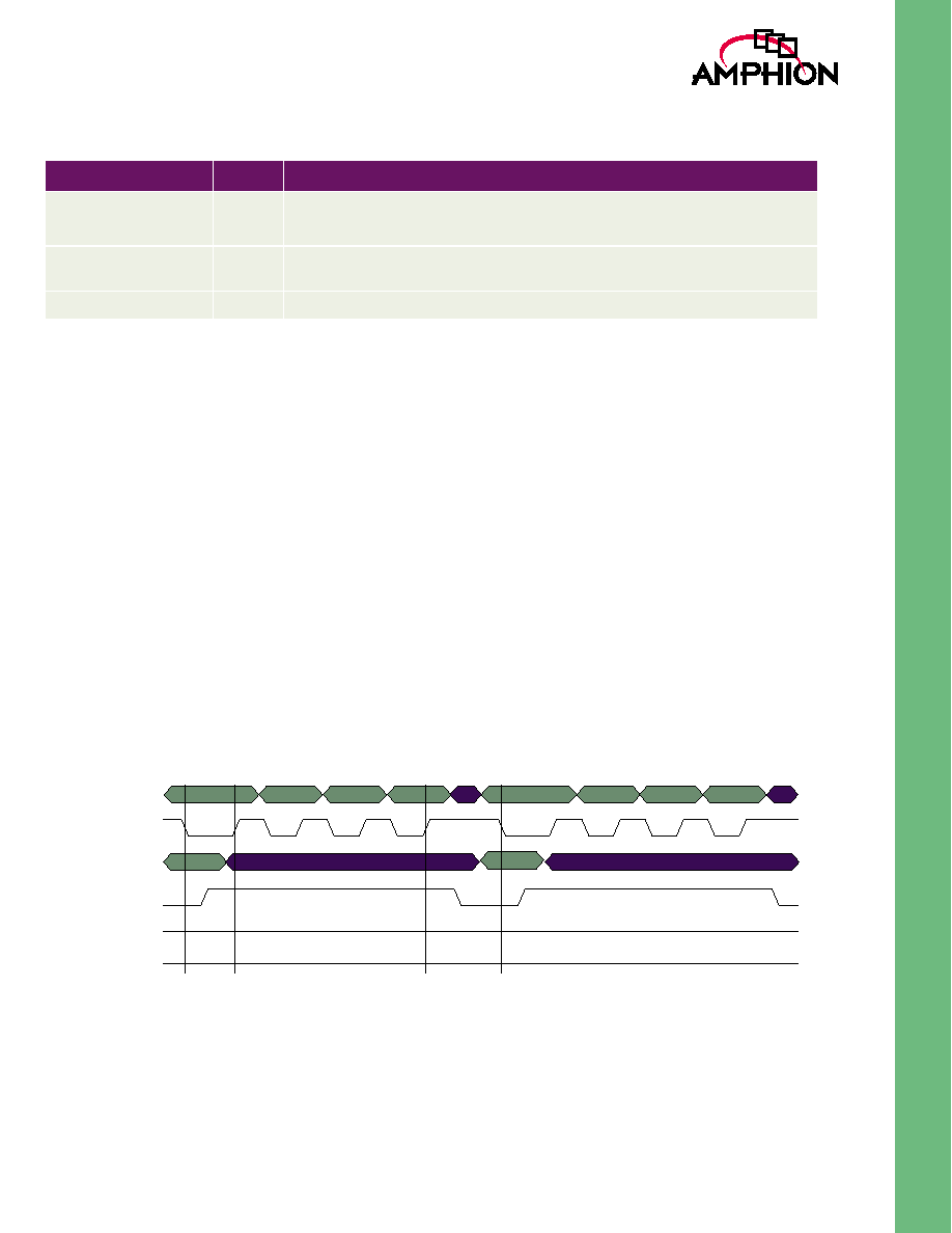
PICTURE-OUT INTERFACE
The Picture-Out interface handshakes out pixel data (in either
RGB or YCbCr format). The display order of objects are set
from the Picture_Out_interface_control register or implied
by the priorities of the objects in the Vid_Obj_Layer_1_objn
registers.
P_DataAvail, the data available indicator, is set as soon as the
full frame for a time instant, all objects, is decoded. Then data
is burst out at a rate controlled by the external handshaking of
the P_DataStrobe line
In Figure 7, pixel data is sent out in 8-bit mode and thus could
either be RGB or YCbCr formats depending on the previous
configuration of the picture out control register. The data of
3C-52-A7 comprises the last pixel in the VOP. The two bits of
P_DataType indicate the sample type currently being output
on P_DataOut, either RGB or YCbCR formats. This waveform
shows P_DataAvail is not asserted for the clock tick before the
last coefficient in the previous group completes. During this
time the P_Data and P_DataType values are undefined, and
P_DataStrobe is ignored. Also, the initial clock ticks of the 3C
and 52 values are not accepted by the external logic,
P_DataStrobe is not asserted, so the CS6750 continues to drive
those old values for another clock tick.
In this example the sample set is the last in the current VOP
(and thus row), so P_VOP_Done and P_VOP_Row_Done are
asserted and the context changes to the next object.
Figure 7: 8-bit Picture-Out Interface Timing
Note: When P_Data port is in 24-bit mode, both pins of the P_DataType[1:0] port are held high.
00
00
80
00
00
11
H_Busy
H_Select[1:0]
H_Strobe
H_Data_In[7:0]
H_ACK_n
H_DDIR
3E
FE
97
6F
H_Data_Out[7:0]
A
B
C
D
5F
3C
52
A7
10
00
01
10
Clk
P_DataOut[7:0]
P_DataType[1:0]
P_DataAvail
P_DataStrobe
P_VOP_Row_Done
P_VOP_Done
00
01
P_Object[1:0]

11
TM
AVAILABILITY AND IMPLEMENTATION INFORMATION
ASIC CORES
For applications that require the high performance, low cost and high integration of an ASIC, Amphion delivers application
specific silicon cores that are pre-optimized to a targeted silicon technology by Amphion experts.
The decoder versions have been specified for a particular profile and level combination as detailed in the ISO/IEC14496-2
specification.
Consult your local Amphion representative for product specific performance information, current availability of individual
products, and lead times on ASIC core porting.
Amphion is a member of M4IF. Details of essential patent licensing terms are due to be released by M4IF and MPEGLA in
January 2002. See future publications for further details.
Table 8: CS6750 ASIC Cores
PRODUCT
ID
SILICON
VENDOR
PROCESS
CLOCK
a
(MHZ)
a. Performance figures based on silicon vendor design kit information. ASIC design is pre-layout using vendor-pro-
vided statistical wire loading information, under the following condition: (T
J
= 125∫C, V
cc
-10%)
LOGIC
GATES
b
b. Logic gates do not include clock circuitry.
MEMORY
AVAILABILITY
DECODER
(mm
2
)
PROGRAM &
REGISTER/
SCRATCH
(mm
2
)
FRAME
(bits)
CS6750TK
LEVEL 1
TSMC
180 nm using Artisan
standard Cell libraries
12
70K
0.16
2.94
c
c. This can be combined with the frame memory.
18.6K x 4 x 8
Now
CS6750TK
LEVEL 2
TSMC
180 nm using Artisan
standard Cell libraries
30
70K
0.16
3.16
c
74.25K x 4 x 8
Now
CS6750TK
LEVEL 3
TSMC
180 nm using Artisan
standard Cell libraries
45
70K
0.16
3.16
c
74.25K x 4 x 8
Now

CS6750
MPEG-4 Video Decoder
TM
Virtual Components for the Converging World
CORPORATE HEADQUARTERS
Amphion Semiconductor Ltd
50 Malone Road
Belfast BT9 5BS
Northern Ireland, UK
Tel:
+44 28 9050 4000
Fax:
+44 28 9050 4001
EUROPEAN SALES
Amphion Semiconductor Ltd
CBXII, West Wing
382-390 Midsummer Boulevard
Central Milton Keynes
MK9 2RG England, UK
Tel:
+44 1908 847109
Fax:
+44 1908 847580
WORLDWIDE SALES & MARKETING
Amphion Semiconductor, Inc
2001 Gateway Place, Suite 130W
San Jose, CA 95110
Tel:
(408) 441 1248
Fax:
(408) 441 1239
CANADA & EAST COAST US SALES
Amphion Semiconductor, Inc
Montreal
Quebec
Canada
Tel:
(450) 455 5544
Fax: (450)
455
5543
Web:
www.amphion.com
Email: info@amphion.com
Voyageur Technical Sales Inc
1 Rue Holiday
Tour Est, Suite 501
Point Claire, Quebec
Canada H9R 5N3
Tel:
(514) 693 5009
Fax:
(514) 693 5007
Phoenix Technologies Ltd
3 Gavish Street
Kfar-Saba, 44424
Israel
Tel:
+972 9 7644 800
Fax:
+972 9 7644 801
JASONTECH, INC
Hansang Building, Suite 300
Bangyidong 181-3, Songpaku
Seoul Korea 138-050
Tel:
+82 2 420 6700
Fax:
+82 2 420 8600
SPINNAKER SYSTEMS INC
Hatchobori SF Bldg. 5F 3-12-8
Hatchobori, Chuo-ku
Tokyo 104-0033 Japan
Tel:
+81 3 3551 2275
Fax:
+81 3 3351 2614
SPS-DA PTE LTD
21 Science Park Rd
#03-19 The Aquarius
Singapore Science Park II
Singapore 117628
Tel:
+65 774 9070
Fax:
+65 774 9071
© 2001- 02 Amphion Semiconductor Ltd. All rights reserved.
Amphion, the Amphion logo,"Virtual Components for the Converging World", are trademarks of Amphion Semiconductor Ltd. All others are the property of their
respective owners.
12
04/02 Publication #: DS6750 v1.2
ABOUT AMPHION
Amphion (formerly Integrated
Silicon Systems) is the leading
supplier of speech coding, video/
image processing and channel coding
application specific silicon cores for
system-on-a-chip (SoC) solutions in
the broadband, wireless, and
mulitmedia markets
SALES AGENTS