
Doc. No. 100427B
May 4, 2000
AccessRunner
ADSL-USB
Modem Device Set
Scalable, Discrete Multitone-based, T1.413 Issue 2, G.992.1
(G.dmt), and G.992.2 (G.lite) - Compliant ADSL Modem
Device Set
Data Sheet
Conexant Proprietary Information

AccessRunner ADSL-USB Modem Device Set Data Sheet
ii
Conexant
100427B
Revision History
Revision
Date
Comments
A
1/27/2000
Initial release
B
5/4/2000
Added hardware interface tables and host interface description.
© 2000,
Conexant Systems, Inc.
All Rights Reserved.
Information in this document is provided in connection with Conexant Systems, Inc. ("Conexant") products. These materials are provided by
Conexant as a service to its customers and may be used for informational purposes only. Conexant assumes no responsibility for errors or
omissions in these materials. Conexant may make changes to specifications and product descriptions at any time, without notice. Conexant
makes no commitment to update the information and shall have no responsibility whatsoever for conflicts or incompatibilities arising from
future changes to its specifications and product descriptions.
No license, express or implied, by estoppel or otherwise, to any intellectual property rights is granted by this document. Except as provided in
Conexant's Terms and Conditions of Sale for such products, Conexant assumes no liability whatsoever.
THESE MATERIALS ARE PROVIDED "AS IS" WITHOUT WARRANTY OF ANY KIND, EITHER EXPRESS OR IMPLIED, RELATING TO
SALE AND/OR USE OF CONEXANT PRODUCTS INCLUDING LIABILITY OR WARRANTIES RELATING TO FITNESS FOR A
PARTICULAR PURPOSE, CONSEQUENTIAL OR INCIDENTAL DAMAGES, MERCHANTABILITY, OR INFRINGEMENT OF ANY PATENT,
COPYRIGHT OR OTHER INTELLECTUAL PROPERTY RIGHT. CONEXANT FURTHER DOES NOT WARRANT THE ACCURACY OR
COMPLETENESS OF THE INFORMATION, TEXT, GRAPHICS OR OTHER ITEMS CONTAINED WITHIN THESE MATERIALS.
CONEXANT SHALL NOT BE LIABLE FOR ANY SPECIAL, INDIRECT, INCIDENTAL, OR CONSEQUENTIAL DAMAGES, INCLUDING
WITHOUT LIMITATION, LOST REVENUES OR LOST PROFITS, WHICH MAY RESULT FROM THE USE OF THESE MATERIALS.
Conexant products are not intended for use in medical, lifesaving or life sustaining applications. Conexant customers using or selling
Conexant products for use in such applications do so at their own risk and agree to fully indemnify Conexant for any damages resulting from
such improper use or sale.
The following are trademarks of Conexant Systems, Inc.: ConexantTM, the Conexant C symbol, "What's Next in Communications
Technologies"TM, and AccessRunnerTM. Product names or services listed in this publication are for identification purposes only, and may be
trademarks of third parties. Third-party brands and names are the property of their respective owners.
For additional disclaimer information, please consult Conexant's Legal Information posted at www.conexant.com, which is incorporated by
reference.
Reader Response: Conexant strives to produce quality documentation and welcomes your feedback. Please send comments and
suggestions to tech.pubs@conexant.com. For technical questions, contact your local Conexant sales office or field applications engineer.

AccessRunner ADSL-USB Modem Device Set Data Sheet
100427B
Conexant
iii
Contents
1.
Introduction ....................................................................................................................................................... 1-1
1.1
Overview................................................................................................................................................... 1-1
1.2
Applications .............................................................................................................................................. 1-1
1.3
Features ................................................................................................................................................... 1-3
1.3.1
P5200 USB Interface Controller Features.................................................................................. 1-3
1.3.2
CX11627 ADSL DMT Data Pump Features ............................................................................... 1-3
1.3.3
CX20431 ADSL Analog Front End Features.............................................................................. 1-4
1.3.4
CX20441 ADSL Line Driver Features ........................................................................................ 1-4
1.4
Reference Design..................................................................................................................................... 1-4
2.
System Description........................................................................................................................................... 2-1
2.1
General Description.................................................................................................................................. 2-1
2.1.1
Boot ROM and Power Up Procedure ......................................................................................... 2-1
2.1.2
Serial EEPROM Programming Utility ......................................................................................... 2-1
2.2
ADSL Operation ....................................................................................................................................... 2-1
2.2.1
ADSL Operating Modes ............................................................................................................. 2-1
Full Rate ADSL Modes...................................................................................................... 2-1
G.lite Splitterless Mode ..................................................................................................... 2-1
LAN Mode ......................................................................................................................... 2-1
WAN Mode........................................................................................................................ 2-1
2.2.2
Host Software............................................................................................................................. 2-2
2.2.3
Control Panel ............................................................................................................................. 2-2
2.2.4
Installation Wizard ..................................................................................................................... 2-2
2.3
Device Description ................................................................................................................................... 2-2
2.3.1
P5200 UIC Description............................................................................................................... 2-2
ARM Processor ................................................................................................................. 2-2
External Memory Controller............................................................................................... 2-2
Host Interface.................................................................................................................... 2-3
ADSL Interface.................................................................................................................. 2-3
USB Interface.................................................................................................................... 2-3
LED Interface .................................................................................................................... 2-3
EEPROM Interface............................................................................................................ 2-3
General Purpose Input/Output Interface ........................................................................... 2-3
2.3.2
CX11627 ADDP Description ...................................................................................................... 2-4
ATM Transmission Convergence ...................................................................................... 2-4
Digital Interface ................................................................................................................. 2-4
QAM Encoder/Decoder ..................................................................................................... 2-4
FFT.................................................................................................................................... 2-4
Analog Front End Interface ............................................................................................... 2-4
Microcontroller Interface.................................................................................................... 2-4
2.3.3
CX20431 AFE Description ......................................................................................................... 2-5
2.3.4
CX20441 LD Description............................................................................................................ 2-6
3.
Hardware Interface............................................................................................................................................ 3-1
3.1
P5200 UIC Hardware Interface Signals.................................................................................................... 3-1
3.1.1
P5200 UIC Signal Interface, Pin Assignments, and Signal Definitions ...................................... 3-1
P5200 UIC Electrical and Environmental Specifications .......................................................................... 3-8
3.2
CX11627 ADDP Hardware Interface Signals ......................................................................................... 3-10
3.2.1
CX11627 ADDP Hardware Signals, Pin Assignments, and Signal Definitions ........................ 3-10
3.2.2
CX11627 ADDP Electrical and Environmental Specifications ................................................. 3-17
3.3
CX20431 AFE Hardware Interface Signals ............................................................................................ 3-19
3.3.1
CX20431 AFE Hardware Signals, Pin Assignments, and Signal Definitions ........................... 3-19
3.3.2
CX20431 AFE Electrical and Environmental Specifications .................................................... 3-22

AccessRunner ADSL-USB Modem Device Set Data Sheet
iv
Conexant
100427B
3.4
CX20441 LD Hardware Interface Signals............................................................................................... 3-24
3.4.1
CX20441 LD Hardware Signals, Pin Assignments, and Signal Definitions.............................. 3-24
3.4.2
CX20441 LD Electrical and Environmental Specifications....................................................... 3-27
4.
USB General Operation .................................................................................................................................... 4-1
4.1
Descriptors ............................................................................................................................................... 4-1
4.1.1
Device Descriptor....................................................................................................................... 4-1
4.1.2
Configuration Descriptor ............................................................................................................ 4-3
4.1.3
Interface Descriptor.................................................................................................................... 4-4
4.1.4
Endpoint Descriptor ................................................................................................................... 4-5
4.1.5
Enumeration............................................................................................................................... 4-6
4.1.6
Endpoint Pairs............................................................................................................................ 4-6
4.1.7
Language ID Table..................................................................................................................... 4-6
4.1.8
Manufacturer String Table.......................................................................................................... 4-6
4.1.9
Product ID String Table.............................................................................................................. 4-7
4.1.10
Serial Number String Table........................................................................................................ 4-8
5.
Package Dimensions ........................................................................................................................................ 5-1

AccessRunner ADSL-USB Modem Device Set Data Sheet
100427B
Conexant
v
Figures
Figure 1-1. AccessRunner ADSL-USB Modem Device Set Simplified Hardware Interface...................................................... 1-1
Figure 1-2. AccessRunner ADSL-USB Modem Device Set Major Interfaces ........................................................................... 1-2
Figure 2-1. P5200 UIC Block Diagram ..................................................................................................................................... 2-3
Figure 2-2. CX11627 ADDP Block Diagram ............................................................................................................................. 2-4
Figure 2-3. CX20431 AFE Block Diagram................................................................................................................................ 2-5
Figure 2-4. CX20441 LD Block Diagram .................................................................................................................................. 2-6
Figure 3-1. P5200 UIC Hardware Interface Signals ................................................................................................................. 3-2
Figure 3-2. P5200 UIC Pin Signals-176-Pin TQFP................................................................................................................... 3-3
Figure 3-3. CX11627 ADDP Hardware Interface Signals ....................................................................................................... 3-11
Figure 3-4. CX11627 ADDP Pin Signals - 176-Pin TQFP ...................................................................................................... 3-12
Figure 3-5. CX20431 AFE Hardware Interface Signals .......................................................................................................... 3-19
Figure 3-6. CX20431 AFE Pin Signals - 32-Pin TQFP ........................................................................................................... 3-19
Figure 3-7. CX20441 LD Hardware Interface Signals ............................................................................................................ 3-25
Figure 3-8. CX20441 LD Pin Signals - 32-Pin TQFP.............................................................................................................. 3-25
Figure 5-1. Package Dimensions - 176-Pin TQFP ................................................................................................................... 5-1
Figure 5-2. Package Dimensions - 32-Pin TQFP ..................................................................................................................... 5-2

AccessRunner ADSL-USB Modem Device Set Data Sheet
vi
Conexant
100427B
Tables
Table 1-1. AccessRunner ADSL-USB Modem Device Set Models and Part Numbers ............................................................ 1-2
Table 3-1. P5200 UIC Hardware Signal Definitions.................................................................................................................. 3-4
Table 3-2. P5200 UIC Input/Output Type Descriptions ............................................................................................................ 3-7
Table 3-3. P5200 UIC DC Electrical Characteristics ................................................................................................................ 3-8
Table 3-4. P5200 UIC Operating Conditions ............................................................................................................................ 3-9
Table 3-5. P5200 UIC Absolute Maximum Ratings .................................................................................................................. 3-9
Table 3-6. P5200 UIC Power Consumption.............................................................................................................................. 3-9
Table 3-7. CX11627 ADDP Hardware Signal Definitions ....................................................................................................... 3-13
Table 3-8. CX11627 ADDP Input/Output Type Descriptions .................................................................................................. 3-16
Table 3-9. CX11627 ADDP DC Electrical Characteristics ...................................................................................................... 3-17
Table 3-10. CX11627 ADDP Operating Conditions................................................................................................................ 3-18
Table 3-11. CX11627 ADDP Absolute Maximum Ratings ...................................................................................................... 3-18
Table 3-12. CX11627 ADDP Power Consumption ................................................................................................................. 3-18
Table 3-13. CX20431 AFE Hardware Signal Definitions ........................................................................................................ 3-20
Table 3-14. CX20431 AFE Input/Output Type Descriptions ................................................................................................... 3-21
Table 3-15. CX20431 AFE DC Electrical Characteristics ....................................................................................................... 3-22
Table 3-16. CX20431 AFE Analog Electrical Characteristics................................................................................................. 3-22
Table 3-17. CX20431 AFE Operating Conditions................................................................................................................... 3-23
Table 3-18. CX20431 AFE Absolute Maximum Ratings......................................................................................................... 3-23
Table 3-19. CX20431 AFE Power Consumption .................................................................................................................... 3-23
Table 3-20. CX20441 LD Hardware Signal Definitions........................................................................................................... 3-26
Table 3-21. CX20441 LD Input/Output Type Descriptions ..................................................................................................... 3-26
Table 3-22. CX20441 LD Analog Electrical Characteristics ................................................................................................... 3-27
Table 3-23. CX20441 LD Operating Conditions ..................................................................................................................... 3-27
Table 3-24. CX20441 LD Absolute Maximum Ratings ........................................................................................................... 3-27
Table 3-25. CX20441 LD Power Consumption....................................................................................................................... 3-27
Table 4-1. Device Descriptors .................................................................................................................................................. 4-2
Table 4-2. Configuration Descriptors........................................................................................................................................ 4-3
Table 4-3. Interface Descriptors ............................................................................................................................................... 4-4
Table 4-4. Endpoint Descriptors ............................................................................................................................................... 4-5
Table 4-5. Endpoint Pairs ......................................................................................................................................................... 4-6
Table 4-6. Language ID Table.................................................................................................................................................. 4-6
Table 4-7. Manufacturer String Table....................................................................................................................................... 4-6
Table 4-8. Product ID String Table ........................................................................................................................................... 4-7
Table 4-9. Serial Number String Table ..................................................................................................................................... 4-8

AccessRunner ADSL-USB Modem Device Set Data Sheet
100427B
Conexant
1-1
1. Introduction
1.1 Overview
The Conexant AccessRunner
ADSL-USB Modem Device Set combines an "always-on" high speed Asymmetric Digital
Subscriber Line (ADSL) connection to the telephone line, and Universal Serial Bus (USB) connection to a host PC into a
single cost-effective solution.
Conexant's AccessRunner
ADSL modem device set is compliant with the full-rate ANSI T1.413 Issue 2 and ITU G.dmt
(G.992.1) ADSL standards, and with the splitterless ITU G.lite (G.992.2) specification. This rate-adaptive solution is designed
for Customer Premise Equipment and supports downstream data rates of up to 8 Mbps and upstream data rates of up to 1
Mbps.
The device set takes advantage of the processing power available with today's computers by eliminating the need for a
separate ATM Segmentation and Reassembly (SAR) device, resulting in a cost-effective solution suitable for both full rate and
G.lite applications. Additionally, host-based software provides support for current industry standards for PPP over ATM (RFC
2364) and bridged Ethernet over ATM (RFC 1483) for Windows 98 and Windows 2000.
The USB specification version 1.1 is supported and is the preferred standard method to connect peripherals to PCs.
During periods of no data transmission, the Conexant ADSL DMT data pump performs idle cell insertion and deletion thus
unloading this task from the host PC.
The device set consists of four devices (see Figure 1-1 and Figure 1-2):
∑ USB Interface Controller (UIC), part no. P5200, in a 176-pin TQFP
∑ ADSL DMT Data Pump (ADDP), part no. CX11627, in a 176-pin TQFP
∑ Analog Front End (AFE), part no. CX20431, in a 32-pin TQFP
∑ Line Driver (LD), part no. CX20441, in a 32-pin TQFP
ADSL (Asymmetric Digital Subscriber Line) is a transmission technology used to carry user data over a single twisted pair line
between the Central Office and the Customer Premises. The downstream (Central Office to Customer Premises) direction
typically supports a much higher data rate than the upstream or return (Customer Premises to Central Office) channel. This
asymmetric nature lends itself to applications like remote LAN access, Internet access, and video delivery. The downstream
data rates can go up to 8 Mbps. The upstream data rates can go up to 1 Mbps. Actual data rates depend on the transceiver
implementation, loop length, impairments, and transmitted power.
The Conexant ADSL-USB Modem Device Set is based upon a scalable architecture. This architecture enables the device set
to support splitterless G.lite as well as splittered and splitterless full-rate ADSL. G.lite enables telephone companies to deploy
consumer-oriented, "always on" 1.5 Mbps Internet access services without the need for splitter equipment, micro-filters, or
wiring changes at the customer premises.
1.2 Applications
∑ ADSL Customer Premise Equipment
∑ ADSL USB modems for desktop PCs
∑ ADSL USB modems for notebook PCs
P5200
USB Interface
Controller
(UIC)
176-Pin TQFP
CX11627
ADSL DMT
Data Pump
(ADDP)
176-Pin TQFP
CX20431
Analog Front End
(AFE)
32-Pin TQFP
TIP
RING
100428_F1-1_SID
USB
Interface
TELEPHONE LINE
CX20441
Line Driver
(LD)
32-Pin TQFP
Host-Based
ADSL
Drivers
Device Set
Figure 1-1. AccessRunner ADSL-USB Modem Device Set Simplified Hardware Interface

AccessRunner ADSL-USB Modem Device Set Data Sheet
Conexant
100427B
1-2
Table 1-1. AccessRunner ADSL-USB Modem Device Set Models and Part Numbers
Model/Order/Part Numbers
Marketing Name
Device Set Order No.
USB Interface
Controller (UIC)
[176-pin TQFP]
Part No.
ADSL DMT Data Pump
(ADDP)
[176-pin TQFP]
Part No.
Analog Front End
(AFE)
[32-pin TQFP]
Part No.
Line Driver
(LD)
[32-pin TQFP]
Part No.
AccessRunner
ADSL-USB
Modem Device Set
DSAR-L100-501
P5200-12
CX11627-11
CX20431-21
CX20441-11
SDRAM/SRAM
Required: 2Mbit
SDRAM Options
One 1M x 16 = 2 MB,
Two 2M x 8 = 4 MB, or
One 4M x 16 = 8 MB
Refresh Rate: 15.625 us
SRAM Options
One 128k x 16 = 2 Mbit or
Two 128k x 8 = 2 Mbit
Access Time: 15 ns
CX11627
ADSL DMT
Data Pump
(ADDP)
176-Pin TQFP
CX20431
Analog Front End
(AFE)
32-Pin TQFP
TIP
RING
100428_F1-2_FID
USB
Interface
Telephone
Line
P5200
USB Interface
Controller
(UIC)
176-Pin TQFP
CX20441
Line Driver
(LD)
32-Pin TQFP
ADSL
Software
Drivers
Operating System
Software and
Modem
Communication
Application
Software
Host Computer
EEPROM
Conexant ADSL-USB Modem Device Set
LEDS
Reset Circuit
JTAG Interface
External
Components
Figure 1-2. AccessRunner ADSL-USB Modem Device Set Major Interfaces

AccessRunner ADSL-USB Modem Device Set Data Sheet
100427B
Conexant
1-3
1.3 Features
∑ Complete ADSL-USB solution
∑ Compliant with ADSL standards
-
Full-rate ANSI T1.413 Issue 2 and ITU G.dmt (G.992.1) standards
-
Splitterless ITU G.lite (G.992.2) specification
∑ DMT modulation and demodulation
∑ Full-rate adaptive modem
-
Maximum downstream rate of 8 Mbps
-
Maximum upstream rate of 1 Mbps
∑ Supports splitterless ADSL implementation
∑ WAN mode support: PPP over ATM (RFC 2364)
∑ LAN mode support: bridged Ethernet over ATM (RFC 1483)
∑ Tone detection for low power mode
∑ USB host interface
-
Compliant with USB Specification, Revision 1.1
-
USB full speed (12 Mbps)
-
Suspend/Resume
-
Vendor specific descriptors
-
Bus powered USB device
∑ ATM SAR performed in software driver
1.3.1
P5200 USB Interface Controller Features
∑ CX11627 ADSL DMT Data Pump (ADDP) interface
∑ CX20431 ADSL Analog Front End (AFE) interface
∑ CX20441ADSL Line Driver (LD) interface
∑ Internal USB interface
∑ SDRAM/SRAM interface
∑ LED interface
∑ Serial EEPROM interface
∑ JTAG interface
∑ 176-pin TQFP
1.3.2
CX11627 ADSL DMT Data Pump Features
∑ Low power (0.5W) consumption
∑ DSP-based programmable ADSL data pump
∑ No external Interleave RAM, 16 Kbytes built-in
∑ Echo cancellation
∑ Digital interface and rate buffering
∑ ADSL framing
∑ Forward Error Correction (FEC) encoding and decoding and interleaving
∑ Constellation encoding/decoding
∑ IFFT modulation and FFT demodulation
∑ Transmit and receive signal digital filtering
∑ Time domain equalization
∑ Frequency domain equalization
∑ Clock recovery
∑ CRC and scrambling
∑ Digital interface framing
∑ ATM mode

AccessRunner ADSL-USB Modem Device Set Data Sheet
Conexant
100427B
1-4
∑ Bit-synchronous mode
∑ 176-pin TQFP
1.3.3
CX20431 ADSL Analog Front End Features
∑ Receive signal path includes:
-
Integrated hybrid receiver circuit with programmable gain
-
High pass filtering and 27dB of Automatic Gain Control (AGC) to improve signal-to-echo ratio
-
14-bit ADC
∑ Transmit signal path includes:
-
30dB of AGC for transmit power control
-
Low pass filtering to suppress noise in the receive band
-
14-bit DAC
∑ Independent digital serial data and control interfaces
∑ Low power tone detection mode
∑ 32-pin TQFP
1.3.4
CX20441 ADSL Line Driver Features
∑ Differential input and output line driver
∑ Line impedance matching during power-down
∑ Fixed differential gain
∑ Low power consumption (0.22 W typical)
∑ 32-pin TQFP
1.4 Reference
Design
A reference design for a USB card is available to minimize application design time and costs.
The card is pretested to pass FCC Part 15 and Part 68 for immediate manufacturing.
A design package is available in electronic form. The design package includes files for schematics, bill of materials (BOM),
board layout (Gerber format), and documentation.
The design can also be used for the basis of a custom design by the OEM to accelerate design completion for rapid market
entry.

AccessRunner ADSL-USB Modem Device Set Data Sheet
100427B
Conexant
2-1
2. System
Description
2.1 General
Description
The ADSL - USB modem solution hardware connects to the host PC via USB interface. The complete chipset and system
software is provided. The OEM adds a crystal circuit, EEPROM, RAM, LEDs, and other discrete components. All software to
support a full rate and/or G.lite ADSL modem is provided. Additionally, a control panel providing connection and system
status, an installation wizard providing automatic provisioning, a serial EEPROM programming utility, and a manufacturing
test program are provided.
2.1.1
Boot ROM and Power Up Procedure
The P5200 USB Interface Controller (UIC) contains a boot loader in internal ROM. Upon power up, the P52 UIC reads the
vendor specific USB descriptor information from EEPROM, and then enumerates with the host PC. EEPROM is required so
that USB descriptor information can be supplied during the enumeration process.
2.1.2
Serial EEPROM Programming Utility
The OEM-supplied serial EEPROM is required to store the USB device, configuration, interface, and endpoint descriptors. A
DOS-based EEPROM Programming Utility is available for the OEM to use to program the serial EEPROM with USB device,
configuration, interface, and endpoint descriptors. The USB device descriptors (including Vendor ID, Product ID, Device
Release Number, Manufacturer Name, Product Name, and Serial Number) can be customized as required.
2.2 ADSL
Operation
2.2.1
ADSL Operating Modes
Full Rate ADSL Modes
Both T1.413 and G.992.1 (G.dmt) line coding schemes are supported for downstream rates up to 8 Mbps and upstream rates
up to 1 Mbps in 32 kbps increments. User selection of mode is supported through the provided control panel, however, auto-
provisioning is supported so that the appropriate modulation is automatically selected based on what is supported by the DSL
Access Multiplexer (DSLAM) at the Central Office. When operating in one of the full rate modes, the low and high frequency
bands must be separated with a filter. This can be done with either a service provider-installed splitter (known as "splittered
ADSL"), or with the use of distributed micro-filters in line with each POTS device on the circuit (known as "splitterless full-rate
ADSL"). Both deployment models are supported.
G.lite Splitterless Mode
G.992.2 (G.lite) splitterless mode is supported for downstream rates up to 1.5 Mbps and upstream rates up to 512 kbps in 32
kbps increments. User selection of mode is supported through the provided control panel, however, auto-provisioning is
supported so that the appropriate modulation is automatically selected based on what is supported by the DSLAM at the
Central Office. When operating in splitterless mode, the low and high frequency bands do not need to be separated with a
filter, and neither a service provider installed splitter, nor distributed micro-filters are required.
G.lite mode supports power management by defining a set of power management states for the link and the use of the
Embedded Operations Channel (eoc) to coordinate between the ATU-R and ATU-C.
LAN Mode
RFC-1483, bridged Ethernet over ATM, is supported in the LAN driver. This protocol provides LLC encapsulation for carrying
network interconnect traffic over a single ATM AAL5 Virtual Connection. LLC encapsulation is desirable when it is not
practical to have a separate VC for each carried protocol, such as with an ATM network that only supports Permanent Virtual
Circuits (PVCs). The provided NDIS 5 drivers automatically establish a "connection-less" call using the defined PVC, and
encapsulate Ethernet bridged frames.
WAN Mode
RFC-2364, PPP over ATM, is supported in the WAN driver. Point-to-Point Protocol provides a method of transporting multi-
protocol packets over point-to-point links. Point-to-point links allow for services such as Link Control Protocol, Network-layer
Control Protocol, and authentication. The PPP over ATM standard brings these point-to-point services to the ATM network
where they are not inherently supported. The provided NDIS 5 drivers accept an empty dial string on a specific "link" or PVC
from Windows Dial-up Networking to establish a call, and encapsulate PPP frames.

AccessRunner ADSL-USB Modem Device Set Data Sheet
Conexant
100427B
2-2
User selection of WAN or LAN mode can be done manually via the provided control panel. However, auto-configuration is
supported with the provided installation wizard, so that the protocol mode is selected properly without user intervention.
2.2.2 Host
Software
The host software NDIS miniport driver provided implements the ATM Adaptation Layer 5 (AAL5), which is composed of two
sublayers: 1) the Segmentation and Reassembly (SAR) layer, and 2) the Convergence Sublayer (CS). The AAL5 protocol
provides virtual connections, which offer error detection, but not error correction, between end stations attached to the same
network.
The SAR sublayer transmitter segments the higher layer information into a size suitable for the payload of the ATM cells of a
virtual connection. The receiver reassembles the contents of the cells of a virtual connection into data units to be delivered to
higher layers. During periods of no data transmission, the device set, and not the host software driver, performs idle cell
insertion and deletion, thus unloading this task from the host PC and unburdening the USB with unnecessary traffic.
The Convergence Sublayer performs message identification and clock recovery. Additionally, the CS of the AAL converts the
user service information coming from the upper layer into a protocol data unit (PDU), and also carry out the opposite process
at the receiver.
Unspecified Bit Rate (UBR) service is supported. It allows a connection to be established without specifying the bandwidth
expected from the connection. The network makes no guarantees for UBR service: it establishes the route but does not
commit bandwidth. UBR can be used for applications that have no delivery constraints and do their own error and flow
control. Examples of potential uses or UBR are e-mail and file transfer, as neither application has real-time characteristics.
2.2.3 Control
Panel
A Windows Control Panel Applet is provided to monitor and control ADSL line and call activity, accumulate ADSL line and call
statistics, and identify the software and connection information. The control panel provides different levels of information: 1)
User, 2) Advanced User, 3) Developer. It is intended that only the User level information, which consists of basic connection
statistics such as line rate and connect status, is available to the end user. Other information available to the Advanced User
and Developer include Physical Layer Statistics, ATM Link Statistics, AAL Link Statistics, Protocol setup, and a logging
capability, which collects performance data and logs it to disk.
2.2.4 Installation
Wizard
A Windows Installation Wizard is provided to ease the user's provisioning of the ADSL service. The Wizard allows the user to
select a service provider allowing the associated setup profile to automatically ensure proper setup and installation of the
software drivers. The profiles, based on input from various ADSL service providers, are provided to facilitate deployment and
to minimize user involvement in provisioning ADSL service. A profile contains configuration information for physical layer
options, ATM layer parameters, AAL layer parameters, and TCP/IP layer parameters.
2.3 Device
Description
2.3.1
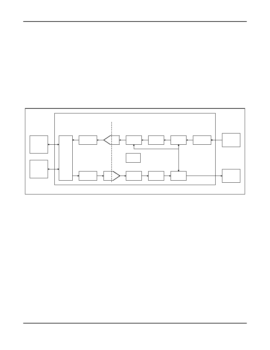
P5200 UIC Description
The P5200 USB Interface Controller (UIC) is the bridge device between the CX11627 ADSL DMT Data Pump (ADDP) and the
host computer. It provides the control, interface, and data manipulation for the CX11627 ADDP, the CX20431 Analog Front
End (AFE), the CX20441 Line Driver (LD), and hybrid circuitry.
The P5200 has output ports for LED indicators and an interface to serial EEPROM for storing vendor specific descriptors. The
UIC conforms to the USB Specification Rev. 1.1 and supports full-speed (12 Mbps) USB device implementation.
The P5200 operates from +1.8V for core operation and +3.3V for interface circuit operation. The P5200 can operate with
+3.3V interface signals (VGG = +3.3V) or +5V interface signals (VGG = +5V).
ARM Processor
The ARM Processor provides the controller and supervisory tasks of the ADSL-USB system. It moves data between the USB
port and the ADSL interface. Control code for the ARM is executed from external memory under control of the External
Memory Controller (EMC).
External Memory Controller
The External Memory Controller (EMC) provides a 16-bit interface to support up to 8 Mbytes of external memory. SDRAM or
SRAM is supported to maintain lowest cost of external memory. There can be 1 (16 bits wide) or 2 (8 bits wide) memories that
can reside on the EMC bus. This bus is not shared with any other functions so activity on this bus can be concurrent with
asynchronous and independent USB port or ADSL data transfers.

AccessRunner ADSL-USB Modem Device Set Data Sheet
100427B
Conexant
2-3
ADSL
Interface
ARM Processor
Control Logic
Host
Interface
GPIO
RAM
ROM
USB
Interface
External
Memory
Controller
(EMC)
SDRAM
or SRAM
USB
ADSL
Data Pump
and AFE
100427 F2-1_BD_P5200
EEPROM
Interface
EEPROM
Figure 2-1. P5200 UIC Block Diagram
Host Interface
The Host Interface is a 16-bit data and 21-bit address bus used for control of the ADSL Data Pump.
ADSL Interface
The ADSL Interface is responsible for data transfer to and from the ADSL Data Pump and the setup of the AFE.
USB Interface
The USB Interface is responsible for data transfer to and from the USB, by extracting clock and data from the USB cable. It
also handles the front end functions of the USB protocol such as Sync Field Identification, NRZI-NRZ Conversion, Bit
Stripping and Stuffing, and CRC functions. Additionally, the USB port converts the serial packet to 8-bit parallel data. Control
transfers addressed to End Point Zero are handled by the USB port.
LED Interface
GPIO are used to support the following LED signals: Power, Ready, Showtime, TXD, and RXD.
EEPROM Interface
A 2-wire serial EEPROM is used to store USB device, configuration, interface, and endpoint descriptors. Device descriptors
include Vendor ID, Product ID, Device Release Number, Manufacturer Name, Product Name, and Serial Number. Both 4196
bit and 2048 bit EEPROMs are supported. The EEPROM speed must be capable of 400 kHz clock frequency.
A typical 4196 bit (512 x 8) EEPROM that meets P5200 UIC requirements is the Fairchild M24C04M8 or equivalent.
A typical 2048 bit (256 x 8) EEPROM that meets P5200 UIC requirements is the Fairchild M24C02M8 or equivalent.
General Purpose Input/Output Interface
Most General Purpose Input/Output (GPIO) pins are programmed for dedicated system functions or reserved for test or
growth functions and are not available for user assignment. Each GPIO pin is controlled individually for input/output direction.
All GPIO pins can serve as external interrupt inputs.

AccessRunner ADSL-USB Modem Device Set Data Sheet
Conexant
100427B
2-4
2.3.2
CX11627 ADDP Description
The CX11627 ADSL DMT Data Pump (ADDP) is a T1.413 Issue 2, G.992.1, and G.992.2 compliant custom digital signal
processing (DSP) chip built specifically for DMT ADSL transmission for use in ADSL modems. The CX11627 operates from
+2.5V for core operation and +3.3V for interface circuit operation. A block diagram of the CX11627 ADDP is shown in Figure
2-2.
ATM Transmission Convergence
In the transmit direction, the ATM Transmission Convergence (TC) block embeds ATM cells into the serial data stream being
fed into the digital interface, i.e., the P5200 UIC. In the receive direction, this block extracts the ATM cell boundaries from the
serial data stream coming from the digital interface To reduce traffic on the USB, the TC block performs idle cell insertion in
the transmit direction and idle cell deletion and header error correction in the receive direction.
Digital Interface
The Digital Interface (DI) Transmit Block performs the following functions: transmit data multiplexing and buffering, fast and
interleave data stream framing, transmit data synchronization control, eoc/aoc insertion, CRC encoding, scrambling, FEC
encoding, and data interleaving.
The DI Receive Block performs the following functions: data de-interleaving, FEC decoding, descrambling, CRC check,
receive data synchronization and receive clock generation, demultiplexing and buffering of receive data and receive eoc/aoc.
QAM Encoder/Decoder
The QAM Encoder/Decoder performs the following functions: constellation encoding, clock recovery, receive gain
compensation, frequency domain equalization (FEQ), slicing, and constellation decoding. The block also performs other
functions such as frequency domain signal processing, signal power, error power averaging and computations related to
frequency domain training.
FFT
The FFT performs IFFT for modulation of the transmit symbol, and FFT for demodulation of the receive symbol.
Analog Front End Interface
The Analog Front End (AFE) interface performs the following functions: transmit signal filtering, time domain equalization, and
time domain signal power averaging, and echo cancellation (EC).
Microcontroller Interface
The microcontroller interface enables the P5200 UIC to set parameters to control DSP sequencing and to read/write
coefficients or data.
DI
Transmit
Block
DI
Receive
Block
Digital
Interface (DI)
Bit
Parser
and QAM
Encoder
QAM
Decoder
and Bit
Parser
QAM Encoder/Decoder
FEQ
IFFT
FFT
FFT
Transmit
Filter
Time
Domain
Equalizer
ADC
Intf
AFE Interface
DAC
Intf
Microcontroller
Interface
EC
P5200
USB
Interface
Controller
(UIC)
ATM
TC
CX20431
Analog
Front End
(AFE)
100427 F2-2 BD 11627
CX11627 ADSL DMT Data Pump (ADDP)
Figure 2-2. CX11627 ADDP Block Diagram
AccessRunner ADSL-USB Modem Device Set Data Sheet
100427B
Conexant
2-5
2.3.3
CX20431 AFE Description
The CX20431 Analog Front End (AFE) can support full-rate and G.lite (G.992.2) ADSL modems. The CX20431 AFE
interfaces with the CX20441 LD and the hybrid receive circuitry on the analog side, and with the CX11627 ADDP on the
digital side.
The receive section filters out the unwanted echo and boosts the wanted signal before performing an analog-to-digital (A/D)
conversion.
The transmit section converts digital data to analog signals and performs a smoothing operation before presenting the signals
to the line driver.
Wakeup in G.lite mode is supported by tone detection circuitry integrated in the CX20431 AFE.
The CX20431 operates from a +3.3V supply.
A block diagram of the CX20431 AFE is shown in Figure 2-3.
Reference
Generators
High Pass
Filter
CX20431 Analog Front End (AFE)
Hybrid
OpAmp
Low Pass
Filter
Decimation
Filter
SC Filter
Serial
Interface
Interpolation
Filter
Low Pass
Filter
ADC
AGC
AGC
DAC
Analog Section
Digital Section
P5200
USB
Interface
Controller
(UIC)
100427 F2-3_BD_P20431
CX20441
Line Driver
(LD)
Hybrid
CX11627
ADSL
Data Pump
(ADDP)
Figure 2-3. CX20431 AFE Block Diagram

AccessRunner ADSL-USB Modem Device Set Data Sheet
Conexant
100427B
2-6
2.3.4
CX20441 LD Description
The CX20441 Line Driver (LD) supports full-rate (T1.413 and G.992.1) and G.lite (G.992.2) ADSL modems. It is optimized for
ideal ADSL performance providing low noise, high bandwidth, and superior linearity. The CX20441 LD transmits a DMT
modulated signal in the 25 ≠ 132 kHz band.
The CX20441 LD operates from a +5V supply. Internal load balancing prevents the CX20441 LD from loading the system
when in a power down state. A block diagram of the CX20441 LD is shown in Figure 2-4.
Current Control
Block
248.4
248.4
400
OUTP_DRV
OUTM_DRV
INP_DRV
INM_DRV
RBIAS
100427 F2-4_BD_20441
+
-
+
+
-
-
Figure 2-4. CX20441 LD Block Diagram

AccessRunner ADSL-USB Modem Device Set Data Sheet
100427B
Conexant
3-1
3. Hardware
Interface
3.1
P5200 UIC Hardware Interface Signals
3.1.1
P5200 UIC Signal Interface, Pin Assignments, and Signal Definitions
P5200 UIC hardware interface signals are shown in Figure 3-1.
P5200 UIC pin assignments are shown in Figure 3-2.
P5200 UIC hardware interface signals are defined in Table 3-1. Input/output types are described in Table 3-2.

AccessRunner ADSL-USB Modem Device Set Data Sheet
Conexant
100427B
3-2
USBP
USBN
FCLKIO (GPIO39)
USB_Pwr_Det (GPIO22)
CLKI
BOPT (GPIO14)
PLLBP
HRST#
LED_READY (GPIO07)
LED_SHOWTIME (GPIO18)
LED_TXD (GPIO19)
LED_RXD (GPIO20)
I2C_SCL (GPIO16)
I2C_SDA (GPIO15)
TRST#
TCK
TMS
TDI
TDO
TREQA
VDD
VDD
VDD
VDD
VDDA
VDDO
VDDO
VDDO
VDDO
VDDO
VDDO
VDDO
VDDO
VDDO
VDDO
VDDO
VDDO
VDDO
VDDO
VDDO
VGG
VGG
VSS
VSS
VSS
VSS
VSSO
VSSO
VSSO
VSSO
VSSO
VSSO
VSSO
VSSO
VSSO
VSSO
VSSO
VSSO
VSSO
VSSO
VSSO
VSSA
Reserved (GPIO06)
Reserved (GPIO17)
Reserved (GPIO25)
Reserved
Reserved
Reserved
Reserved
Reserved
Reserved
Reserved
151
152
29
150
27
39
28
98
160
1
176
2
11
12
31
32
33
34
35
36
25
66
99
154
21
8
16
37
47
57
71
81
91
107
117
127
137
147
158
171
23
101
26
67
100
155
9
17
38
48
58
72
82
92
108
118
128
138
148
159
172
22
157
175
68
13
14
15
18
19
20
24
+3.3V
BCLKIO (GPIO38)
PAIR_SEL (GPIO21)
LD_OH_DET (GPIO05)
LD_PC (GPIO13)
AFE_RST# (GPIO08)
AFE_SCLK
AFE_STB
AFE_CTRLIN
AFE_CTRLOUT
AFE_WAKEUP
RXSOC0
RCLKAS0
RDATAS0
TXSOC0
TCLKLS0
TDATLS0
RST# (GPIO09)
IRQ0 (GPIO10)
IRQ1 (GPIO11)
PD (GPIO12)
SCANMODE (GPIO26)
HAD00
HAD01
HAD02
HAD03
HAD04
HAD05
HAD06
HAD07
HAD08
HAD09
HAD10
HAD11
HAD12
HAD13
HAD14
HAD15
HC01
HC02
HC03
HC04
HC05
HC06
HC07
HAD16
HAD17
HAD18
HC08
HC09
HC12 (GPIO34)
HA10
HAD19
HAD20
HAD21
HAD22
HAD23
HAD24
HAD25
HAD26
HAD27
HAD28
HAD29
HC00 (GPIO32)
FLASH_RST# (GPIO23)
HC11 (GPIO33)
HAD31 (GPIO37)
MB0
MB1
MA00
MA01
MA02
MA03
MA04
MA05
MA06
MA07
MA08
MA09
MA10
MA11
MD00
MD01
MD02
MD03
MD04
MD05
MD06
MD07
MD08
MD09
MD10
MD11
MD12
MD13
MD14
MD15
MM1
MM0
MCLK
MCKE
MRAS#
MCAS#
MWE#
MCS#
30
3
156
166
161
4
7
10
5
6
168
169
167
173
174
170
162
163
164
165
153
88
87
86
85
84
83
80
79
78
77
76
75
74
73
70
65
64
63
62
61
60
59
56
55
54
53
96
95
89
94
52
51
50
49
46
45
44
43
42
41
40
93
97
90
69
149
146
145
144
143
142
141
140
139
136
135
134
133
132
121
120
119
116
115
114
113
112
111
110
109
106
105
104
103
102
124
125
122
123
126
129
131
130
CX20441 LD
100427_F3-01_HIS P5200 176T
P5200
USB Interface
Controller
(UIC)
176-PIN TQFP
SDRAM
or
SRAM
USB
INTERFACE
USB PWR DETECT
LED
INTERFACE
CLOCK
RESET CIRCUIT
EEPROM
JTAG
+3.3V OR +5V
+1.8V
+1.8V THROUGH FILTER
GND
NC
CX20431 AFE
CX11627 ADDP
SERIAL
INTERFACE
CX11627 ADDP
PARALLEL
INTERFACE
RECEIVE PAD
I/O PAIR SEL
ROH#
PWRDWN# (OPTIONAL)
PWRDWN#
POR#
STROBE
CTRL_STRB
CTRL_IN
CTRL_OUT
WAKEUP
RXSOC0
R_NCO_AS0
R_DAT_AS0
TXSOC0
T_CLK_LS0
T_DAT_LS0
RSTB
IRQ1
IRQ2
PWR_DWN
SSCANMODE
D00
D01
D02
D03
D04
D05
D06
D07
D08
D09
D10
D11
D12
D13
D14
D15
A0
A1
A2
A3
A4
A5
A6
A7
A8
A9
RDB
WRB
CSB
BA0
BA1
A0
A1
A2
A3
A4
A5
A6
A7
A8
A9
A10
A11
D0
D1
D2
D3
D4
D5
D6
D7
D8
D9
D10
D11
D12
D13
D14
D15
DQMH
DQML
CLK
CLKE
RAS#
CAS#
WE#
CS#
CX11627 ADDP
CONTROL
4.7K
NC
1 K
NC
A10
A11
A12
A13
A14
A15
A16
A17
A18
A19
A20
OE#
RESET#
NC
NC
LINE
INTERFACE
USB Resume
NC
Figure 3-1. P5200 UIC Hardware Interface Signals

AccessRunner ADSL-USB Modem Device Set Data Sheet
100427B
Conexant
3-3
100427F3-02 PO-P50-176T
1
2
3
4
5
6
7
8
9
10
11
12
13
14
15
16
17
18
19
20
21
22
23
24
25
26
27
28
29
30
31
32
33
34
35
36
37
38
39
40
41
42
43
44
45
46
47
48
49
50
51
52
53
54
55
56
57
58
59
60
61
62
63
64
65
66
67
68
69
70
71
72
73
74
75
76
77
78
79
80
81
82
83
84
85
86
87
88
132
131
130
129
128
127
126
125
124
123
122
121
120
119
118
117
116
115
114
113
112
111
110
109
108
107
106
105
104
103
102
101
100
99
98
97
96
95
94
93
92
91
90
89
176
175
174
173
172
171
170
169
168
167
166
165
164
163
162
161
160
159
158
157
156
155
154
153
152
151
150
149
148
147
146
145
144
143
142
141
140
139
138
137
136
135
134
133
LED_SHOWTIME (GPIO18)
LED_RXD (GPIO20)
PAIR_SEL (GPIO21)
AFE_SCLK
AFE_CTRLOUT
AFE_WAKEUP
AFE_STB
VDDO
VSSO
AFE_CTRLIN
I2C_SCL (GPIO16)
I2C_SDA (GPIO15)
Reserved
Reserved
Reserved
VDDO
VSSO
Reserved
Reserved
Reserved
VDDA
VSSA
VGG
Reserved
VDD
VSS
CLKI
PLLBP
FCLKIO (GPIO39)
BCLKIO (GPIO38)
TRST#
TCK
TMS
TDI
TDO
TREQA
VDDO
VSSO
BOPT (GPIO14)
HAD29
HAD28
HAD27
HAD26
HAD25
MA11
MWE#
MCS#
MCAS#
VSSO
VDDO
MRAS#
MM0
MM1
MCKE
MCLK
MD00
MD01
MD02
VSSO
VDDO
MD03
MD04
MD05
MD06
MD07
MD08
MD09
MD10
VSSO
VDDO
MD11
MD12
MD13
MD14
MD15
VGG
VSS
VDD
HRST#
FLASH_RST# (GPIO23)
HC08
HC09
HC10
HC00 (GPIO32)
VSSO
VDDO
HC11 (GPIO33)
HC12 (GPIO34)
LED_TXD (GPIO19)
Reserved (GPIO17)
TCLKLS0
TXSOC0
VSSO
VDDO
TDATLS0
RCLKAS0
RXSOC0
RDATAS0
LD_PC (GPIO13)
PD (GPIO12)
IRQ1 (GPIO11)
IRQ0 (GPIO10)
RST# (GPIO09)
AFE_RST# (GPIO08)
LED_READY (GPIO07)
VSSO
VDDO
Reserved (GPIO06)
LD_OH_DET (GPIO05)
VSS
VDD
SCANMODE (GPIO26)
USBN
USBP
USB_Pwr_Det (GPIO22)
MB0
VSSO
VDDO
MB1
MA00
MA01
MA02
MA03
MA04
MA05
MA06
VSSO
VDDO
MA07
MA08
MA09
MA10
HAD24
HAD23
VDDO
VSSO
HAD22
HAD21
HAD20
HAD19
HAD18
HAD17
HAD16
HC07
VDDO
VSSO
HC06
HC05
HC04
HC03
HC02
HC01
HAD15
VDD
VSS
Reserved (GPIO25)
HAD31 (GPIO37)
HAD14
VDDO
VSSO
HAD13
HAD12
HAD11
HAD10
HAD09
HAD08
HAD07
HAD06
VDDO
VSSO
HAD05
HAD04
HAD03
HAD02
HAD01
HAD00
P5200
Figure 3-2. P5200 UIC Pin Signals-176-Pin TQFP

AccessRunner ADSL-USB Modem Device Set Data Sheet
Conexant
100427B
3-4
Table 3-1. P5200 UIC Hardware Signal Definitions
Label
Pin
I/O
I/O Type
Signal Name/Description
USB INTERFACE
USBP,
USBN
151,
152
I/O
Iu/Ou
USB Port. USBP and USBN are the differential data positive and
negative signals of the USB port. Connect USBP and USBN to USB
+Data and -Data, respectively, through 10
, and optionally through a
quick switch in order to isolate the USBP and USBN from the USB
during suspend mode.
FCLKIO (GPIO39)
29
I
It
USB Resume. Active high input used to detect occurrence of USB
resume event.
USB POWER DETECT INTERFACE
USB5V_DET
(GPIO22)
150
I
It
USB 5 V Detect. Active high input used to detect presence of +5 V at
the USB connector.
CLOCK INTERFACE
CLKI
27
I
Ith
Clock In. Connect to 35.328 MHz voltage controlled crystal oscillator
(VCXO) output through 51
.
CONTROL INTERFACE
HRST#
98
I
Ith
Reset. Active low input signal to reset the P5200 UIC. Connect to
reset circuit.
BOPT (GPIO14)
39
I
It
Boot Option. To boot from internal ROM, leave open. To boot from
external ROM, pull down with 4.7k
resistor. Leave open.
PLLBP
28
I
It
PLL Ground. Connect to GND through 4.7 k
.
CX20431 AFE CONTROL AND SERIAL INTERFACE
AFE_SCLK
4
I
It
AFE Clock In. Connect to AFE STROBE through 33
.
AFE_STB
7
O
Otts4
AFE Strobe Out. Connect to AFE CTRL_STRB.
AFE_CTRLIN
10
O
Otts4
AFE Control In. Serial digital data sent to the AFE. Connect to AFE
CTRL_IN.
AFE_CTRLOUT
5
I
It
AFE Control Out. Serial digital data received from the AFE. Connect
to AFE CTRL_OUT.
AFE_WAKEUP
6
I
Ith
AFE Wakeup. DSL Power Management Wakeup Signal from AFE.
Connect to AFE WAKEUP.
CX11627 ADDP PARALLEL INTERFACE
HAD[18:16]
53-55
O
Ot4
Address Lines 9-7. Connect to ADDP A[9:7], respectively.
HC[07:01]
56, 59-64
O
Ot4
Address Lines 6-0. Connect to ADDP A[6:0], respectively.
HAD[15:0]
65, 70, 73-80,
83-88
I/O
It/Ot4
Data Lines 15-00. Connect to ADDP D[15:0], respectively.
HC08
96
O
Ot4
Read Enable. Active low read enable. When asserted, data is
transferred from the selected device onto the data bus. Connect to
ADDP RDB.
HC09
95
O
Ot4
Write Enable. Active low write enable. When asserted, data is
transferred from the data bus into the selected device. Connect to
ADDP WRB.
HC12 (GPIO34)
89
O
O
ADDP Chip Select. Active low output select ADDP when asserted.
Connect to ADDP CSB.
IRQ0#
(GPIO10)
163
I
Itpu
ADDP Interrupt Request 1. Active low input asserted to request
interrupt servicing by the ADDP. Connect to ADDP IRQ1.
IRQ1#
(GPIO11)
164
I
Itpu
ADDP Interrupt Request 2. Active low input asserted to request
interrupt servicing by the ADDP. Connect to ADDP IRQ2.
PD
(GPIO12)
165
O
Ot4
ADDP Power Down. Active low output asserted put ADDP in a low
power mode. Connect to ADDP PWR_DWN.
RST#
(GPIO09)
162
O
Ot4
ADDP Reset. Active low output resets ADDP when asserted. Connect
to ADDP RSTB.
SCANMODE
(GPIO26)
153
O
Ot4
Scan Mode. Connect to ADDP SSCANMODE.

AccessRunner ADSL-USB Modem Device Set Data Sheet
100427B
Conexant
3-5
Table 3-1. P5200 UIC Hardware Signal Definitions (Continued)
Label
Pin
I/O
I/O Type
Signal Name/Description
CX11627 ADDP SERIAL CHANNEL INTERFACE
RXSOC0
168
I
Itpu
Receive ATM0 Start of Cell. Connect to ADDP RXSOC0.
RCLKAS0
169
I
Itpu
Receive AS0/ATM0 Data Clock. Connect to ADDP R_CLK_LS0.
RDATAS0
167
I
Itpu
Receive AS0/ATM0 Serial Data. Connect to ADDP R_DAT_LS0.
TXSOC0
173
O
Otts4
Transmit ATM0 Start of Cell. Connect to ADDP TXSOC0.
TCLKLS0
174
I
It
Transmit LS0/ATM0 Data Clock. Connect to ADDP T_CLK_LS0.
TDATLS0
170
O
Otts4
Transmit LS0/ATM0 Serial Data. Connect to ADDP T_DAT_LS0.
CX20431 AFE AND CX20441 LD CONTROL
AFE_RST#
(GPIO08)
161
O
Ot4
AFE Reset. Active low reset output to the AFE and the LD. Connect
to AFE POR# and to LD PWRDWN#.
LD_PC
(GPIO13)
166
O
Ot4
Line Driver Power Control. Optionally, connect to LD PWRDWN#
when it is desired to power down only the LD.
LINE INTERFACE
LD_OH_DET
(GPIO05)
156
I
It
Off-Hook Detect. Active low; indicates POTS off-hook event. Used
for G.lite Mode only. Connect to off-hook detector circuit.
PAIR_SEL
(GPIO21)
3
O
Itpu/Ot4
Inner/Outer Pair Select. Connect to wire-pair selection circuit.
BCLKIO (GPIO38)
30
O
Itpu/Ot4
Receive Pad. Connect to receive pad circuitry in hybrid.
SERIAL EEPROM INTERFACE
I2C_SCL (GPIO16)
11
O
Ot4
Serial EEROM Clock. Connect to EEPROM clock input.
I2C_SDA (GPIO15)
12
I
Itpu
Serial EEROM Data. Connect to EEPROM data line.
JTAG INTERFACE
TRST#
31
I
Itpu
JTAG Reset. A high-to-low transition on this signal forces the TAP
controller into a logic reset state. This pin has an internal pullup, and it
conforms to IEEE 1149.1 JTAG specification.
TCK
32
I
It
JTAG Test Clock. This is the boundary scan clock input signal. This
pin has an internal pullup, and it conforms to IEEE 1149.1 JTAG
specification.
TMS
33
I
Itpu
JTAG Test Mode Select. This signal controls the operation of the
TAP controller. This pin has an internal pull-up, and it conforms to
IEEE 1149.1 JTAG specification.
TDI
34
I
Itpu
JTAG Test Input. This signal contains serial data that is shifted in on
the rising edge of TCK. The pin has an internal pullup, and it conforms
to IEEE 1149.1 JTAG specification.
TDO
35
O
Otts4
JTAG Test Output Data. This is the three-stateable boundary scan
data output signal from the MCU, and it is shifted out on the falling
edge of TCK. It conforms to IEEE 1149.1 JTAG specification.

AccessRunner ADSL-USB Modem Device Set Data Sheet
Conexant
100427B
3-6
Table 3-1. P5200 UIC Hardware Signal Definitions (Continued)
Label
Pin
I/O
I/O Type
Signal Name/Description
SDRAM/SRAM INTERFACE
MA[11:00]
132-136, 139-145
O
Ot4
Multiplexed Row and Column Address Lines. Connect to
SDRAM/SRAM A[11:0], respectively.
MD[15:00]
102-106, 109-
116, 119-121
I/O
It/Ot4
Data Lines. Connect to SDRAM/SRAM D[15:0], respectively.
MB0
149
O
Ot4
Bank Address Select 0. Connect to SDRAM/SRAM Bank Address
Select 0 input for 8 MB SDRAM; leave open for 2 MB SDRAM.
MB1
146
O
Ot4
Bank Address Select 1. Connect to SDRAM/SRAM Bank Address
Select 1 input.
MM1
124
O
Ot4
Input/Output Mask 1. Connect to SDRAM/SRAM I/O Mask High
input.
MM0
125
O
Ot4
Input/Output Mask 0. Connect to SDRAM/SRAM I/O Mask Low
input.
MCLK
122
O
Ot4
SDRAM Clock. Connect to SDRAM Clock input.
MCKE
123
O
Ot4
SDRAM Clock Enable. Active high; enables SDRAM clock. Connect
to SDRAM Clock Enable input.
MRAS#
126
O
Ot4
SDRAM Row Address Strobe. Active low; starts SDRAM access
with strobe of row address. Connect to SDRAM RAS input.
MCAS#
129
O
Ot4
SDRAM Column Address Strobe. Active low; strobes column
address and data bytes. Connect to SDRAM CAS input.
MWE#
131
O
Ot4
SDRAM Memory Write Enable. Active low; indicates write access to
SDRAM. Connect to SDRAM Write Enable input.
MCS#
130
O
Ot4
SDRAM Memory Chip Select. Active low; enables SDRAM
command decoder. Connect to SDRAM chip select input.
LED INTERFACE
LED_RXD
(GPIO20)
2
O
Ot4
Receive Data LED. Illuminated when data is received from the ADSL
line.
LED_TXD
(GPIO19)
176
O
Ot4
Transmit Data LED. Illuminated when data is transmitted to the
ADSL line.
LED_SHOWTIME
(GPIO18)
1
O
Ot4
Showtime LED. Illuminated when the ADSL transceiver is in
Showtime Mode.
LED_READY
(GPIO070)
160
O
Ot4
Ready LED. Illuminated when the device is successfully enumerated
on the USB.
POWER AND GROUND
VDD
25, 66, 99, 154
PWR
PWR
Core Supply Voltage. Connect to +1.8V.
VDDA
21
PWR
PWR
Supply Voltage. Connect to +1.8V through filter.
VDDO
8, 16, 37, 47, 57,
71, 81, 91, 107,
117, 127, 137,
147, 158, 171
PWR
PWR
I/O Supply Voltage. Connect to +3.3V.
VGG
23, 101
REF
REF
I/O Clamp Power Supply. Connect to +5V if available, otherwise
connect to +3.3V.
VSS
26, 67, 100, 155
GND
GND
Core Ground. Connect to digital ground.
VSSO
9, 17, 38, 48, 58,
72, 82, 92, 108,
118, 128, 138,
148, 159, 172
GND
GND
I/O Ground. Connect to digital ground.
VSSA
22
GND
GND
Ground. Connect to digital ground.

AccessRunner ADSL-USB Modem Device Set Data Sheet
100427B
Conexant
3-7
Table 3-1. P5200 UIC Hardware Signal Definitions (Continued)
Label
Pin
I/O
I/O Type
Signal Name/Description
NOT USED
HC10
94
I
It
Not Used. Connect to GND through 1 K
.
HAD[29:19]
40-46, 49-52
O
Ot4
Address Lines 20-10. If Flash ROM is installed, connect to Flash
ROM A[20:10], respectively. If Flash ROM is not installed, leave open.
HC00 (GPIO32)
93
O
Ot4
Flash ROM Chip Enable. Active low output enables optional Flash
ROM when asserted. If Flash ROM is installed, connect to Flash ROM
CE#. If Flash ROM is not installed, leave open.
FLASH_RST#
(GPIO23)
97
O
Ot4
Flash ROM Reset. Active low output resets optional Flash ROM
when asserted. If Flash ROM is installed, connect to Flash ROM
RESET#. If Flash ROM is not installed, leave open.
HC11 (GPIO33)
90
I/O
It/Ot4
Not Used. Leave open.
HAD31 (GPIO37)
69
I/O
It/Ot4
Not Used. Leave open.
TREQA
36
I
Itpd
Reserved. This pin is connected to internal circuitry. Leave open.
Reserved (GPIO06)
157
I/O
Itpu/Ot4
Reserved. This pin is connected to internal circuitry. Leave open.
Reserved (GPIO17)
175
I/O
Itpu/Ot4
Reserved. This pin is connected to internal circuitry. Leave open.
Reserved (GPIO25)
68
I/O
Itpu/Ot4
Reserved. This pin is connected to internal circuitry. Leave open.
Reserved
13-15, 18-20, 24
Reserved. These pins are connected to internal circuitry. Leave open.
NOTES:
I/O Types: See Table 3-2.
Table 3-2. P5200 UIC Input/Output Type Descriptions
I/O Type
Description
It
Digital input, +5V tolerant, CIN = 8 pF
It/Ot4
Digital input, +5V tolerant, CIN = 8 pF/Digital output, 4 mA, ZINT = 80
Ith
Digital input, +5V tolerant, with hysteresis, CIN = 8 pF
Itpd
Digital input, +5V tolerant, 75k
pull-down, CIN = 8 pF
Itpu
Digital input, +5V tolerant, 75k
pull-up, CIN = 8 pF
Itpu/Ot4
Digital input, +5V tolerant, 75k
pull-up, CIN = 8 pF/Digital output, 4 mA, ZINT = 80
Otts4
Digital output, 3-State, 4 mA, ZINT =80
Iu/Ou
Input, USB receiver/Output, USB driver
NOTES:
1. See DC characteristics in Table 3-3.
2. I/O Type corresponds to the device Pad Type. The I/O column in tables refers to signal I/O direction used in the application.

AccessRunner ADSL-USB Modem Device Set Data Sheet
Conexant
100427B
3-8
P5200 UIC Electrical and Environmental Specifications
P5200 UIC DC electrical characteristics are listed Table 3-3.
P5200 UIC operating conditions are specified in Table 3-4.
P5200 UIC absolute maximum ratings are stated in Table 3-5.
P5200 UIC power consumption is listed in Table 3-6.
Table 3-3. P5200 UIC DC Electrical Characteristics
Parameter
Symbol
Min.
Typ.
Max.
Units
Test Conditions
(see Note 1)
Input high voltage
VIH
2.0
VGG + 0.5
VDC
Input low voltage
VIL
-0.5
0.8
VDC
Input leakage current
IIL/IIH
-10
10
µA
VIN = 0 for Min.
VIN = VIN (MAX) for Max.
Input leakage current (with internal
pull-downs) (See Note 2)
IIL/IIH
-10
100
µA
VIN = 0 for Min.
VIN = VIN (MAX) for Max.
Input leakage current (with internal
pull-ups) (See Note 2)
IIL/IIH
-100
10
µA
VIN = 0 for Min.
VIN = VIN (MAX) for Max.
Internal pullup/pulldown resistance
Rpu/Rpd
50
200
k
Output high voltage
VOH
2.4
VDDO
VDC
IOH = 4 mA
Output low voltage
VOL
0.4
VDC
IOL = 4 mA
Input/output capacitance
CINOUT
3
pF
NOTES:
1. Test Conditions (unless otherwise stated):
VDDcore = +1.8 ± 0.15 VDC
VDDO = +3.3 ± 0.3 VDC;
VIN (MAX) = +3.6V for VGG connected to +3.3V;
VIN (MAX) = +5.25V for VGG connected to +5V.
2. Current flow out of the device is shown as minus.
3. Stresses above those listed may cause permanent device failure. Functionality at or above these limits is not implied. Exposure to
absolute maximum ratings for extended periods of time may affect device reliability.

AccessRunner ADSL-USB Modem Device Set Data Sheet
100427B
Conexant
3-9
Table 3-4. P5200 UIC Operating Conditions
Parameter
Symbol
Min
Typ
Max
Units
Core power supply
VDD
1.65
1.8
1.95
VDC
I/O power supply
VDDO
3.0
3.3
3.6
VDC
Operating ambient temperature
TA
0
70
∞C
Table 3-5. P5200 UIC Absolute Maximum Ratings
Parameter
Symbol
Min
Max
Units
Core power supply
VDD
-0.35
2.0
VDC
I/O power supply (VDDO = +3.3 V)
VDDO
-0.35
3.7
VDC
I/O power supply (VDDO = +5 V)
VDDO
-0.35
7.0
VDC
Input voltage
VIN
-0.35
VGG + 0.35*
VDC
Voltage applied to outputs in high impedance (Off)
state
VHZ
-0.35
VGG + 0.35*
VDC
Storage temperature
TS
-55
125
∞C
* VGG = +3.3 V ± 0.3 V or +5 V ± 0.25 V.
Caution: Handling CMOS Devices
These devices contain circuitry to protect the inputs against damage due to high static voltages. However, it is advised that
normal precautions be taken to avoid application of any voltage higher than maximum rated voltage.
An unterminated input can acquire unpredictable voltages through coupling with stray capacitance and internal cross talk.
Both power dissipation and device noise immunity degrades. Therefore, all inputs should be connected to an appropriate
supply voltage.
Input signals should never exceed the voltage range from 0.5V or more negative than GND to 0.5V or more positive than
VDD. This prevents forward biasing the input protection diodes and possibly entering a latch up mode due to high current
transients.
Table 3-6. P5200 UIC Power Consumption
Mode
Typ. Current
(mA)
Max. Current
(mA)
Typ. Power
(mW)
Max. Power
(mW)
VDD (+1.8 V)
85
105
155
205
VDDO (+3.3 V)
15
25
45
90
NOTES:
1. Operating voltage: VDD = +1.8 VDC ± 0.15 VDC
VDDO = +3.3 VDC ± 0.3 VDC.
2. Test conditions:
VDD = +1.8 VDC for typical values; VDD = +1.95 VDC for maximum values.
VDDO = +3.3 VDC for typical values; VDDO = +3.6 VDC for maximum values.

AccessRunner ADSL-USB Modem Device Set Data Sheet
Conexant
100427B
3-10
3.2
CX11627 ADDP Hardware Interface Signals
3.2.1
CX11627 ADDP Hardware Signals, Pin Assignments, and Signal Definitions
CX11627 ADDP hardware interface signals are shown in Figure 3-3.
CX11627 ADDP pin assignments are shown in Figure 3-4.
CX11627 ADDP hardware interface signals are defined in Table 3-7. Input/output types are described in Table 3-9.

AccessRunner ADSL-USB Modem Device Set Data Sheet
100427B
Conexant
3-11
MCLK
VCXO_CTRL
RXSOC0
R_NCO_AS0
T_CLK_AS1
R_DAT_AS0
TXSOC0
T_CLK_LS0
T_DAT_LS0
RSTB
IRQ1
IRQ2
PWR_DN
SSCANMODE
A0
A1
A2
A3
A4
A5
A6
A7
A8
A9
D00
D01
D02
D03
D04
D05
D06
D07
D08
D09
D10
D11
D12
D13
D14
D15
CSB
RDB
WRB
TLXCK_EN
VDDO
VDDO
VDDO
VDDO
VDDO
VDDO
VDDO
VDDO
VDDO
VDDO
VDDO
VDDO
VDDO
VDDcore
VDDcore
VDDcore
VDDcore
VDDcore
VDDcore
VDDcore
VDDcore
VDDcore
VDDcore
VDDcore
VDDcore
VDDcore
VDDcore
VGG
VSSO
VSSO
VSSO
VSS
VSS
VSSO
VSSO
VSSO
VSS
VSS
VSS
VSSO
VSS
VSS
VSS
VSSO
VSSO
VSS
VSS
VSS
VSSO
VSSO
VSS
VSSO
VSS
VSS
VSS
VSSO
VSSO
VSS
68
66
45
39
11
41
21
15
16
85
83
82
79
55
102
101
100
99
98
97
96
95
94
91
127
126
125
124
123
120
119
118
117
116
115
114
113
112
111
104
87
86
90
22
10
27
36
54
69
76
89
110
122
132
156
168
176
25
26
59
60
61
70
71
93
108
109
134
140
154
155
103
1
9
18
19
20
28
35
52
53
62
63
64
72
73
74
75
88
92
105
106
107
121
131
133
139
151
152
153
167
175
RX00
RX08
TX15
AFE_STRB
TEST_START
TEST_DONE
MON_CLK
MON_OUT
MON_DONE
TX00
TX01
TX02
TX03
TX04
TX05
TX06
TX07
TX08
TX09
TX10
TX11
TX12
TX13
TX14
RX01
RX02
RX03
RX04
RX05
RX06
RX07
RX09
RX10
RX11
RX12
RX13
RX14
RX15
DMCK_ALT
T_INTER_BYTEB
T_FAST_BYTEB
T_CLK_AS0
T_DAT_AS1
T_DAT_AS0
T_DAT_LS1
T_DAT_LS1
BIT_CLOCK
TXSOC1
LTR
NTR
NTRCTL
FILTER_CLK
DAC_CLK
R_INTER_SUPERB
R_INTER_DATA
R_FAST_SUPERB
R_FAST_FRAMEB
R_NCO_LS0
R_NCO_LS1
R_NCO_AS1
R_DAT_AS1
R_CLK_LS0
R_CLK_LS1
R_DAT_LS0
R_DAT_LS1
RXSOC1
ADC_CLK
CLIPB
SCANEN
NC
NC
NC
NC
NC
129
143
174
24
58
56
78
77
67
157
158
159
160
161
162
163
164
165
166
169
170
171
172
173
130
135
136
137
138
141
142
144
145
146
147
148
149
150
30
5
4
6
12
7
13
14
17
23
81
8
29
3
2
31
32
33
34
37
38
40
42
47
49
48
50
46
128
84
65
43
44
51
57
80
100427_F3-03_HIS 11627 176T
CX20431 AFE
SERIAL
INTERFACE
CX11627
ADSL DMT Data Pump
(ADDP)
176-PIN TQFP
P5200 UIC
PARALLEL BUS
NC
CLK OUT
CLK CTRL
RXSOC0
RCLKAS0
RDATAS0
TXSOC0
TCLKLS0
TDATLS0
RST# (GPIO09)
IRQ0 (GPIO10)
IRQ1 (GPIO11)
PD (GPIO12
SCANMODE
HC01
HC02
HC03
HC04
HC05
HC06
HC07
HAD16
HAD17
HAD18
HAD00
HAD01
HAD02
HAD03
HAD04
HAD05
HAD06
HAD07
HAD08
HAD09
HAD10
HAD11
HAD12
HAD13
HAD14
HAD15
HC12
HC08
HC09
+3.3V
+2.5V
+5V or +3.3V
P5200 UIC
CONTROL
P5200 UIC
SERIAL
INTERFACE
35. 328 MHZ
CLOCK
TEST
INTERFACE
RX0
RX1
TX0
STROBE
NC
NC
NC
NC
NC
MONITOR
INTERFACE
Figure 3-3. CX11627 ADDP Hardware Interface Signals

AccessRunner ADSL-USB Modem Device Set Data Sheet
Conexant
100427B
3-12
100427 F3-04 PO-11627-176T
1
2
3
4
5
6
7
8
9
10
11
12
13
14
15
16
17
18
19
20
21
22
23
24
25
26
27
28
29
30
31
32
33
34
35
36
37
38
39
40
41
42
43
44
45
46
47
48
49
50
51
52
53
54
55
56
57
58
59
60
61
62
63
64
65
66
67
68
69
70
71
72
73
74
75
76
77
78
79
80
81
82
83
84
85
86
87
88
132
131
130
129
128
127
126
125
124
123
122
121
120
119
118
117
116
115
114
113
112
111
110
109
108
107
106
105
104
103
102
101
100
99
98
97
96
95
94
93
92
91
90
89
176
175
174
173
172
171
170
169
168
167
166
165
164
163
162
161
160
159
158
157
156
155
154
153
152
151
150
149
148
147
146
145
144
143
142
141
140
139
138
137
136
135
134
133
VSSO
DAC_CLK
FILTER_CLK
T_FAST_BYTEB
T_INTER_BYTEB
T_CLK_AS0
T_DAT_AS0
NTR
VSSO
VDDO
T_CLK_AS1
T_DAT_AS1
T_DAT_LS1
T_DAT_LS1
T_CLK_LS0
T_DAT_LS0
BIT_CLOCK
VSSO
VSS
VSS
TXSOC0
TLXCK_EN
TXSOC1
AFE_STRB
VDDcore
VDDcore
VDDO
VSSO
NTRCTL
DMCK_ALT
R_INTER_SUPERB
R_INTER_DATA
R_FAST_SUPERB
R_FAST_FRAMEB
VSSO
VDDO
R_NCO_LS0
R_NCO_LS1
R_NCO_AS0
R_NCO_AS1
R_DAT_AS0
R_DAT_AS1
NC
NC
VDDO
VSS
RX01
RX00
ADC_CLK
D00
D01
D02
D03
D04
VDDO
VSSO
D05
D06
D07
D08
D09
D10
D11
D12
D13
D14
VDDO
VDDcore
VDDcore
VSSO
VSS
VSS
D15
VGG
A0
A1
A2
A3
A4
A5
A6
A7
A8
VDDcore
VSS
A9
WRB
VDDO
VDDO
VSS
TX15
TX14
TX13
TX12
TX11
TX10
VDDO
VSSO
TX09
TX08
TX07
TX06
TX05
TX04
TX03
TX02
TX01
TX00
VDDO
VDDcore
VDDcore
VSSO
VSS
VSS
RX15
RX14
RX13
RX12
RX11
RX10
RX09
RX08
RX07
RX06
VDDcore
VSS
RX05
RX04
RX03
RX02
VDDcore
VSSO
RXSOC0
RXSOC1
R_CLK_LS0
R_DAT_LS0
R_CLK_LS1
R_DAT_LS1
NC
VSSO
VSS
VDDO
SSCAN_MODE
TEST_DONE
NC
TEST_START
VDDcore
VDDcore
VDDcore
VSS
VSS
VSSO
SCAN_EN
VCXO_CTRL
MON_DONE
MCLK
VDDO
VDDcore
VDDcore
VSS
VSS
VSS
VSSO
VDDO
MON_OUT
MON_CLK
PWR_DN
NC
LTR
IRQ2
IRQ1
CLIPB
RSTB
RDB
CSB
VSSO
CX11627
Figure 3-4. CX11627 ADDP Pin Signals - 176-Pin TQFP

AccessRunner ADSL-USB Modem Device Set Data Sheet
100427B
Conexant
3-13
Table 3-7. CX11627 ADDP Hardware Signal Definitions
Signal Name
Pin
I/O
I/O Type
Signal Name/Description
CLOCK INTERFACE
MCLK
68
I
I
Master Clock In. Connect to 35.328 MHz voltage controlled crystal
oscillator (VCXO) output through 51
.
VXCO_CTRL
66
O
O
VCXO Control Out. Oversampled VCXO analog control voltage
output. Connect to VCXO control circuit.
CX20431 AFE INTERFACE
RX[15:0]
150-144, 142-
141, 138-135,
130-129
I
I
Receive Data Lines. In the serial mode of operation, RX8 and RX0
transfer data from the AFE into the ADDP. The negative edge of the
AFE_STR# strobe signal from the AFE clocks the data into the
ADDP.
In the parallel mode of operation, RX[15:0] input data lines transfer
receive data into the ADDP. Data is clocked into the ADDP by
ADC_CLK. This mode is not used; leave RX[15:9] and RX[7:1] open.
TX[15:0]
174-169, 166-157
O
O
Transmit Data Lines. In the serial mode of operation, TX15 (used as
a programmable width serial bus) transfers data to the AFE from the
ADDP. The negative edge of the AFE_STR# strobe signal from the
AFE clocks the data from the ADDP.
In the parallel mode of operation, TX[15:0] output data lines transfer
data out of the ADDP. Data is clocked out of the ADDP by DAC_CLK.
This mode is not used; leave TX[14:0] open.
AFE_STR#
I
I
AFE Strobe. In the serial mode of operation, AFE_STR# from the
AFE triggers the transfer of serial transmit data on TX15 from the
ADDP to the AFE and triggers the transfer of serial receive data on
RX8 and RX0 from the AFE to the ADDP.
ADC_CLK
128
O
O
Receive Clock for Parallel Mode. In the parallel mode of operation,
data on RX[15:0] is clocked in to the ADDP by ADC_CLK. Not used;
leave open.
DAC_CLK
2
O
O
Transmit Clock for Parallel Mode. In the parallel mode of operation,
data on TX[15:0] is clocked out of the ADDP by DAC_CLK. Not used;
leave open.
FILTER_CLK
3
O
O
AFE Filter Clock. This signal can be used by the DAC interface block
to strobe the external AFE filters. Not use; leave open
P5200 UIC PARALLEL INTERFACE
D[15:0]
104, 111-120,
123-127
I/O
It/Ot
Data Bus. A 16-bit input/output data bus used to send data to the UIC
during a read operation or receive data from the UIC during a write
operation. Connect to D[15:0] to UIC HAD[15:0], respectively.
A[9:0]
91, 94-102
I
It
Address Bus. A 10-bit input address bus that identifies the location in
the ADDP that data on D[15:0] is written to during a write operation, or
that data is read from during a read operation for placing on D[15:0].
Connect A[9:7] to UIC HC[18:16], respectively and A[6:0] to UIC
HC[07:01], respectively.
CS#
87
I
It
Chip Select. Active low control input selects the ADDP. Connect CS#
to UIC HC12.
RD#
86
I
It
Data Read Enable. Active low control input strobes (on the negative
edge) data from the addressed location in the ADDP onto D[15:0].
Connect RD# to UIC HC08.
WR#
90
I
It
Data Write Enable. Active low control input strobes (on the negative
edge) data on D[15:0] into the ADDP addressed location. Connect
WR# to UIC HC09.

AccessRunner ADSL-USB Modem Device Set Data Sheet
Conexant
100427B
3-14
Table 3-7. CX11627 ADDP Hardware Signal Definitions (Continued)
Signal Name
Pin
I/O
I/O Type
Signal Name/Description
P5200 UIC CONTROL
RSTB
85
I
I
Reset. Active low control input. When asserted, the ADDP is held in a
reset state. Connect to UIC RST# (GPIO09).
IRQ1
83
O
Ot
Interrupt Request 1. Active high interrupt asserted to request service
by the UIC. Connect to UIC IRQ0 (GPIO10).
IRQ2
82
O
Ot
Interrupt Request 2. Active high interrupt asserted to request service
by the UIC. Connect to UIC IRQ1 (GPIO11).
PWR_DN
79
I
I
Power Down. Active high control input When asserted, the ADDP is
held in a low power mode. Connect to UIC PD (GPIO12).
SSCANMODE
55
I
I
Scan Mode. Connect to UIC SCANMODE (GPIO26).
TLXCK_EN
22
I
I
LSX Transmit Data Clock Generation Enable. Connect to +3.3V.
P5200 UIC SERIAL INTERFACE
RXSOC0
45
O
O
TC0 Block Receive Start of Cell. Connect to UIC RXSOC0.
R_DAT_AS0
41
O
O
Receive Data (AS0). Connect to UIC RDATAS0.
R_NCO_AS0
39
O
O
Receive NCO (AS0). Connect to UIC RCLKAS0.
T_CLK_AS1
11
I
I
Transmit Data Clock (AS1). Connect to ADDP NCO_AS0.
T_CLK_LS0
15
I/O
I/O
Transmit Data Clock (LS0). Connect to UIC TCLKLS0.
T_DAT_LS0
12
I
I
Transmit Data (LS0). Connect to UIC TDATLS0.
TXSOC0
21
I
I
TC0 Block Transmit Start of Cell. Connect to UIC TXSOC0.
MONITOR INTERFACE
MON_OUT
77
O
O
Monitor Output. 1-bit serial D/A output used for constellation
monitoring. Used for test only; leave open during normal operation.
MON_CLK
78
O
O
Monitor Clock. Serial monitor 138 kHz clock output. Used for test
only; leave open during normal operation.
MON_DONE
67
O
O
Monitor Done. New symbol constellation qualifier. Used for test only;
leave open during normal operation.
POWER AND GROUND
VDDcore
25, 26, 59, 60, 61,
70, 71, 93, 108,
109, 134, 140,
154, 155
P
PWR
Core Circuits Supply Voltage. Connect to +2.5V supply.
VDDO
10, 27, 36, 54, 69,
76, 89, 110, 122,
132, 156, 168,
176
P
PWR
Input/Output Circuits Supply Voltage. Connect to +3.3V supply.
VSS
19, 20, 53, 62, 63,
72, 73, 74, 92,
105, 106, 131,
139, 151, 152,
175
G
GND
Core Circuits Ground. Connect to digital ground.
VSSO
1, 9, 18, 28, 35,
52, 64, 75, 88,
107, 121, 133,
153, 167
G
GND
Input/Output Circuits Ground. Connect to digital ground.
VGG
103
R
R
Input Reference Voltage. Reference voltage for +5V tolerant input
pins. A connection to +5V allows +5V or +3.3V input levels. A
connection to +3.3V allows +3.3V input levels only.

AccessRunner ADSL-USB Modem Device Set Data Sheet
100427B
Conexant
3-15
Table 3-7. CX11627 ADDP Hardware Signal Definitions (Continued)
Signal Name
Pin
I/O
I/O Type
Signal Name/Description
NOT USED
R_INTER_SUPERB
31
O
O
Receive Interleaved Data Bit Output Superframe Qualifier. Not
used; leave open.
R_INTER_DATA
32
O
O
Receive Interleaved Data Bit Output. Clocked at BIT_CLOCK rate.
R_FAST_SUPERB
33
O
O
Receive Fast Data Bit Output Superframe Qualifier. Not used;
leave open.
R_FAST_FRAMEB
34
O
O
Receive Fast Data Bit Output Frame Qualifier. Not used; leave
open.
R_CLK_LS0
47
I
I
Receive Data Clock (LS0). Not used; leave open.
R_CLK_LS1
49
I
I
Receive Data Clock (LS1). Not used; leave open.
R_DAT_AS1
42
O
O
Receive Data (AS1). Not used; leave open.
R_DAT_LS0
48
O
O
Receive Data (LS0). Not used; leave open.
R_DAT_LS1
50
O
O
Receive Data (LS1). Not used; leave open.
R_NCO_AS1
40
O
O
Receive NCO (AS1). Not used; leave open.
R_NCO_LS0
37
O
O
Receive NCO (LS0). Not used; leave open.
R_NCO_LS1
38
O
O
Receive NCO (LS1). Not used; leave open.
CLIPB
84
O
O
Clip Interrupt. This status output goes low for one ADC_CLK clock
cycle whenever clipping is detected. This signal can be for monitoring
incoming data for saturation. Not used; leave open.
T_INTER_BYTEB
5
O
O
Transmit Interleaved Data Bit Input Enable. Not used; leave open.
T_FAST_BYTEB
4
O
O
Transmit Fast Data Bit Input Enable. Not used; leave open.
T_CLK_AS0
6
I
I
Transmit Data Clock (AS1). Not used; leave open.
T_DAT_AS1
12
I
I
Transmit Data (AS1). Not used; leave open.
T_DAT_AS0
7
I
I
Transmit Data (AS0). Not used; leave open.
T_CLK_LS1
13
I/O
I/O
Transmit Data Clock (LS1). Not used; leave open.
T_DAT_LS1
14
I
I
Transmit Data (LS1). Not used; leave open.
TXSOC1
21
I
I
TC1 Block Transmit Start of Cell. Not used; leave open.
LTR
81
O
O
8 kHz Local Timing Reference. Not used; leave open.
NTR
8
I/O
I/O
8 kHz Network Timing Reference. Not used; leave open.
NTR_CTL
29
I
I
Network Timing Reference I/O Control. Not used; leave open.
BIT_CLOCK
17
O
O
Serial Data Bit Clock Output. Used to synchronize the serial input
and output data bit streams, enables, and superframe qualifiers. Not
used; leave open.
NOTES:
I/O Types: See Table 3-8.

AccessRunner ADSL-USB Modem Device Set Data Sheet
Conexant
100427B
3-16
Table 3-8. CX11627 ADDP Input/Output Type Descriptions
I/O Type
Description
It
Digital input, +5 V tolerant, CIN = 8 pF
It/Ot4
Digital input, +5 V tolerant, CIN = 8 pF/Digital output, 4 mA, ZINT = 80
Ith
Digital input, +5 V tolerant, with hysteresis, CIN = 8 pF
Itpd
Digital input, +5 V tolerant, 75k
pull-down, CIN = 8 pF
Itpu
Digital input, +5 V tolerant, 75k
pull-up, CIN = 8 pF
Itpu/Ot4
Digital input, +5 V tolerant, 75k
pull-up, CIN = 8 pF/Digital output, 4 mA, ZINT = 80
Otts4
Digital output, 3-State, 4 mA, ZINT =80
NOTES:
1. See DC characteristics in Table 3-9.
2. I/O Type corresponds to the device Pad Type. The I/O column in tables refers to signal I/O direction used in the application.

AccessRunner ADSL-USB Modem Device Set Data Sheet
100427B
Conexant
3-17
3.2.2
CX11627 ADDP Electrical and Environmental Specifications
CX11627 ADDP DC electrical characteristics are listed in Table 3-9.
CX11627 ADDP operating conditions are specified in Table 3-10.
CX11627 ADDP absolute maximum ratings are stated in Table 3-11.
CX11627 ADDP power consumption is listed in Table 3-12.
Table 3-9. CX11627 ADDP DC Electrical Characteristics
Parameter
Symbol
Min.
Typ.
Max.
Units
Test Conditions
(see Note 1)
Input high voltage
VIH
0.9*VDDO
VDDO
VDC
Input low voltage
VIL
GND
0.1*VDDO
VDC
Input leakage current
IIL/IIH
-10
10
µA
Input capacitance
CIN
2.9
pF
Output high voltage
VOH
0.9*VDDO
VDDO
VDC
Output low voltage
VOL
GND
0.1*VDDO
VDC
Three-state output leakage
ILK
10
10
µA
Output capacitance
COUT
3.1
pF
Three-state output leakage
ILK
-10
10
µA
Input/output capacitance
CINOUT
3.9
pF
NOTES:
1. Test Conditions (unless otherwise stated):
VDDcore = +2.5 ± 0.2 VDC
VDDO = +3.3 ± 0.3 VDC;
VIN (MAX) = +3.6 for VGG connected to +3.3V;
VIN (MAX) = +5.25V for VGG connected to +5V.
2. Current flow out of the device is shown as minus.

AccessRunner ADSL-USB Modem Device Set Data Sheet
Conexant
100427B
3-18
Table 3-10. CX11627 ADDP Operating Conditions
Parameter
Symbol
Min
Typ
Max
Units
Core power supply
VDDcore
2.3
2.5
2.7
VDC
I/O power supply
VDDO
3.0
3.3
3.6
VDC
Operating temperature
TA
0
+70
∞C
Table 3-11. CX11627 ADDP Absolute Maximum Ratings
Parameter
Symbol
Min
Max
Units
Core power supply
VDDcore
-0.35
2.8
VDC
I/O power supply
VDDO
-0.35
3.7
VDC
Input voltage
VIN
-0.3
VDD + 0.3
VDC
Storage temperature
TS
-65
150
∞C
Table 3-12. CX11627 ADDP Power Consumption
Mode
Typ. Current
(mA)
Max. Current
(mA)
Typ. Power
(mW)
Max. Power
(mW)
VDDcore (+2.5 V)
190
210
475
570
VDDO (+3.3 V)
35
65
115
235
NOTES:
1. Operating voltage: VDDcore = +2.5 VDC ± 0.2 VDC
VDDO = +3.3 VDC ± 0.3 VDC.
2. Test conditions:
VDDcore = +2.5 VDC for typical values; VDDcore = +2.7 VDC for maximum values.
VDDO = +3.3 VDC for typical values; VDDO = +3.6 VDC for maximum values

AccessRunner ADSL-USB Modem Device Set Data Sheet
100427B
Conexant
3-19
3.3
CX20431 AFE Hardware Interface Signals
3.3.1
CX20431 AFE Hardware Signals, Pin Assignments, and Signal Definitions
CX20431 AFE hardware interface signals are shown in Figure 3-5.
CX20431 AFE pin assignments are shown in Figure 3-6.
CX20431 AFE hardware interface signals are defined in Table 3-13. DC characteristics are listed in Table 3-15.
CLKIN
CTRL_STRB
CTRL_IN
CTRL_OUT
WAKEUP
POR
RX0
RX1
TX0
STROBE
DVDD
AVDD
AVDD
AVSS
AVSS
DVSS
DVSS
DVSS
11
15
16
17
18
13
24
23
22
19
21
5
9
6
10
14
25
27
INP_HYBR_RX
INM_HYBR_RX
OUTP_TX
OUTM_TX
VREFP
VC
VREFM
RBIAS
INP_RX
INM_RX
NC
NC
NC
NC
1
2
7
8
29
30
31
32
3
4
12
20
26
28
100427_F3-05_HIS 20431 32T
HYBRID
CX20431
ANALOG FRONT END
(AFE)
32-PIN TQFP
P5200 UIC
CX11627 ADDP
+3.3V
+3.3V through filter
0.1u
F
10
uF
0.1u
F
10
uF
0.1u
F
10
uF
30K
NC
CX20441 LD
INP_DRV
INM_DRV
AFE_SCLK
AFE_STB
AFE_CTRLIN
AFE_CTRLOUT
AFE_WAKEUP
AFE_RST#
RX00
RX08
TX00
AFE_STRB
Figure 3-5. CX20431 AFE Hardware Interface Signals
100427_F3-06 PO_20431_32T
1
2
3
4
5
6
7
8
9
10
11
12
13
14
15
16
32
31
30
29
28
27
26
25
24
23
22
21
20
19
18
17
INP_HYBR_RX
INM_HYBR_RX
INP_RX
INM_RX
AVDD
AVSS
OUTP_TX
OUTM_TX
RX0
RX1
TX0
DVDD
NC
STROBE
WAKEUP
CTRL_OUT
AVDD
AVSS
CLKIN
NC
POR
DVSS
CTRL_STRB
CTRL_IN
RBIAS
VREFM
VC
VREFP
NC
DVSS
NC
DVSS
CX20431
Figure 3-6. CX20431 AFE Pin Signals - 32-Pin TQFP

AccessRunner ADSL-USB Modem Device Set Data Sheet
Conexant
100427B
3-20
Table 3-13. CX20431 AFE Hardware Signal Definitions
Signal Name
Pin
I/O
I/O Type
Signal Name/Description
CLOCK INTERFACE
CLKIN
11
I
It
Clock In. Connect to 35.328 MHz voltage controlled crystal oscillator
(VCXO) output through 51
.
P5200 UIC CONTROL AND CX11627 ADDP SERIAL INTERFACE
CTRL_STRB
15
I
It
Strobe In. Strobe input for the control interface. Connect to UIC
AFE_STB.
CTRL_IN
16
I
It
Control In. Serial digital data received from the UIC. Connect to UIC
AFE_CTRLIN.
CTRL_OUT
17
O
Ot
Control Out. Serial digital data sent to the UIC. Connect to UIC
AFE_CTRLOUT.
WAKEUP
18
O
Ot
Wakeup. Digital output for tone detection mode. Connect to UIC
AFE_WAKEUP.
POR#
13
I
It
Reset. Active low power-On reset. Connect to UIC AFE_RST#.
P5200 UIC CONTROL AND CX11627 ADDP SERIAL INTERFACE
STROBE
19
O
Ot
Strobe. Strobe output for the data interface. The negative STROBE
edge triggers the transfer of serial transmit data on TX0 from the
ADDP to the AFE and triggers the transfer of serial receive data on
RX0 and RX1 from the AFE to the ADDP. Connect to ADDP
AFE_STRB and to UIC AFE_SCLK.
CX11627 ADDP SERIAL INTERFACE
RX0
24
O
Ot
Receive Data. Digital receive serial data output on RX0 is transferred
to the ADDP. The negative edge of the STROBE signal from the AFE
clocks the data into the ADDP. Connect to ADDP AFE_RX00.
RX1
23
O
Ot
Receive Data. Digital receive serial data output on RX1 is transferred
data to the ADDP. The negative edge of the STROBE signal from the
AFE clocks the data into the ADDP. Connect to ADDP AFE_RX08.
TX0
22
I
It
Transmit Data. Digital transmit serial data input on TX0 is transferred
from the ADDP. The negative edge of the STROBE signal clocks the
data from the ADDP. Connect to ADDP AFE_TX00.
HYBRID INTERFACE
INP_HYBR_RX
1
I
Ia
Receive Input Positive from Hybrid. Receive input positive from the
hybrid circuit. AC couple through 1
µF.
INM_HYBR_RX
2
I
Ia
Receive Input Negative from Hybrid. Receive input negative from
the hybrid circuit. AC couple through 1
µF.
CX20441 LINE DRIVER INTERFACE
OUTP_TX
7
O
Oa
Transmit Output Positive. Transmit output positive to the LD.
Connect to LD INP_DRV.
OUTM_TX
8
O
Oa
Transmit Output Negative. Transmit output negative to the LD.
Connect to LD INM_DRV.
POWER AND GROUND
VREFP
29
REF
REF
Analog Reference Voltage (+2.5V). Connect to GND through 10
µF
and 0.1
µF in parallel.
VC
30
REF
REF
Analog Reference Voltage (+1.5V). Connect to GND through 10
µF
and 0.1
µF in parallel.
VREFM
31
REF
REF
Analog Reference Voltage (+0.5V). Connect to GND through 10
µF
and 0.1
µF in parallel.
RBIAS
32
REF
REF
Analog Current Reference. Current setting external resistor.
Connect to GND through 30 k
resistor (+1%).
DVDD
21
PWR
PWR
Digital Circuits Supply. Connect to +3.3V.
AVDD
5, 9
PWR
PWR
Analog Circuits Supply Voltage. Connect to +3.3V through filter.
DVSS
14, 25, 27
GND
GND
Digital Circuits Ground. Connect to GND.
AVSS
6, 10
AGND
AGND
Analog Circuit Ground. Connect to GND.
AccessRunner ADSL-USB Modem Device Set Data Sheet
100427B
Conexant
3-21
Table 3-3. CX20431 AFE Hardware Signal Definitions (Continued)
Signal Name
Pin
I/O
I/O Type
Signal Name/Description
NOT USED
INP_RX
3
I
Ia
Receive Input Positive. Not used. Leave open.
INM_RX
4
I
Ia
Receive Input Negative. Not used. Leave open.
NC
12, 20, 26, 28
No Connect. These pins are not connected to internal circuitry.
NOTES:
I/O Types: See Table 3-15.
Table 3-14. CX20431 AFE Input/Output Type Descriptions
I/O Type
Description
Ia
Analog input
It
Digital input, +5V tolerant, CIN = 8 pF
It/Ot4
Digital input, +5V tolerant, CIN = 8 pF/Digital output, 4 mA, ZINT = 80
Ith
Digital input, +5V tolerant, with hysteresis, CIN = 8 pF
Itpd
Digital input, +5V tolerant, 75k
pull-down, CIN = 8 pF
Itpu
Digital input, +5V tolerant, 75k
pull-up, CIN = 8 pF
Itpu/Ot4
Digital input, +5V tolerant, 75k
pull-up, CIN = 8 pF/Digital output, 4 mA, ZINT = 80
Oa
Analog Output
Otts4
Digital output, 3-State, 4 mA, ZINT =80
NOTES:
1. See DC characteristics in Table 3-15 and analog electrical characteristics in Table 3-16.
2. I/O Type corresponds to the device Pad Type. The I/O column in tables refers to signal I/O direction used in the application.
AccessRunner ADSL-USB Modem Device Set Data Sheet
Conexant
100427B
3-22
3.3.2
CX20431 AFE Electrical and Environmental Specifications
CX20431 AFE DC electrical characteristics are listed Table 3-15.
CX20431 AFE analog electrical characteristics are listed Table 3-16.
CX20431 AFE operating conditions are specified in Table 3-17.
CX20431 AFE absolute maximum ratings are stated in Table 3-18.
CX20431 AFE power consumption is listed in Table 3-19.
Table 3-15. CX20431 AFE DC Electrical Characteristics
Parameter
Symbol
Min.
Typ.
Max.
Units
Test Conditions
(see Note 1)
Input high voltage
VIH
0.65*VDD
VDD+0.35
VDC
Input low voltage
VIL
-0.35
0.25*VDD
VDC
Input leakage current
IIL
-10
10
µA
Output high voltage
VOH
0.85*VDD
VDD
VDC
Output low voltage
VOL
0
0.1*VDD
VDC
Output leakage current
IOLK
10
10
µA
NOTES:
1. Test Conditions (unless otherwise stated):
DVDD and AVDD = +5.0 ± 0.25 VDC
VIN (MAX) = +5.25V
2. Current flow out of the device is shown as minus.
Table 3-16. CX20431 AFE Analog Electrical Characteristics
Parameter
Min
Typ
Max
Units
Receive Path
Differential input amplitude of in-band signal
2
Vp
Differential input amplitude of echo
2.1
Vp
Input-referred noise density in 170 kHz ≠ 1104 kHz, gain = 27 dB
15
20
nV/sqrt (Hz)
Input-referred noise density in 170 kHz ≠ 1104 kHz, gain = 0 dB
150
nV/sqrt (Hz)
Intermodulation product falling in the downstream band, from an echo tone
with an in band signal, gain = 27 dB
-80
dBFS
Intermodulation product falling in the downstream band, from 2 in band tones,
gain = 0 dB
-80
dBFS
In-band ripple
1.5
dB
Input resistance (single-ended)
85
k
Input capacitance (single-ended)
90
pF
Transmit Path
Differential output amplitude
2
Vp
Output-referred noise density in 25 kHz ≠ 132 kHz
250
300
nV/sqrt (Hz)
Output-referred noise density in 170 kHz ≠ 1104 kHz
20
nV/sqrt (Hz)
Intermodulation product from 2 in band tones
-80
dBV
In-band ripple
1.25
dB
Output resistive load (single-ended)
5
20
k
Output capacitive load (single-ended)
20
pF

AccessRunner ADSL-USB Modem Device Set Data Sheet
100427B
Conexant
3-23
Table 3-17. CX20431 AFE Operating Conditions
Parameter
Symbol
Min
Typ
Max
Units
Power supply
DVDD and AVDD
3.135
3.3
3.465
VDC
Operating ambient temperature
TA
0
70
∞C
Table 3-18. CX20431 AFE Absolute Maximum Ratings
Parameter
Symbol
Min
Max
Units
Power supply
DVDD and AVDD
-0.35
3.6
VDC
Digital input voltage
VIN
-0.35
DVDD +0.35
VDC
Analog input voltage
VIN
-0.35
AVDD +0.35
VDC
Storage temperature
TS
-65
150
∞C
Table 3-19. CX20431 AFE Power Consumption
Mode
Typ.
Current
(mA)
Max.
Current
(mA)
Typ.
Power
(mW)
Max.
Power
(mW)
DVDD
25
83
AVDD
40.5
134
NOTES:
3. Operating voltage: DVDD and AVDD = +3.3 VDC ± 0.165 VDC.
4. Test conditions:
DVDD and AVDD = +3.3 VDC for typical values; DVDDO and AVDD = +3.465 VDC for maximum values.

AccessRunner ADSL-USB Modem Device Set Data Sheet
Conexant
100427B
3-24
3.4
CX20441 LD Hardware Interface Signals
3.4.1
CX20441 LD Hardware Signals, Pin Assignments, and Signal Definitions
CX20441 LD hardware interface signals are shown in Figure 3-7.
CX20441 LD pin assignments are shown in Figure 3-8.
CX20441 LD hardware interface signals are defined in Table 3-20.

AccessRunner ADSL-USB Modem Device Set Data Sheet
100427B
Conexant
3-25
PWRDWN#
INP_DRV
INM_DRV
AVDD
AVDD
AVSS
AVSS
5
23
2
6
19
8
17
OUTP_DRV
OUTM_DRV
RBIAS
NC
NC
NC
NC
NC
NC
NC
NC
NC
NC
NC
NC
NC
NC
NC
NC
NC
NC
NC
NC
NC
NC
18
7
4
1
3
9
10
11
12
13
14
15
16
20
21
22
24
25
26
27
28
29
30
31
32
100427_F3-7_HIS 20441 32T
HYBRID
CX20441
LINE DRIVER
(LD)
32-PIN TQFP
P5200 UIC
+5V through filter
124K
NC
CX20431 AFE
LD_PC
OUTP_TX
OUTM_TX
Figure 3-7. CX20441 LD Hardware Interface Signals
100427_F3-8 PO_20441_32T
1
2
3
4
5
6
7
8
9
10
11
12
13
14
15
16
32
31
30
29
28
27
26
25
24
23
22
21
20
19
18
17
NC
INM_DRV
NC
RBIAS
PWRDWN#
AVDD
OUTM_DRV
AVSS
NC
INP_DRV
NC
NC
NC
AVDD
OUTP_DRV
AVSS
NC
NC
NC
NC
NC
NC
NC
NC
NC
NC
NC
NC
NC
NC
NC
NC
CX20441
Figure 3-8. CX20441 LD Pin Signals - 32-Pin TQFP

AccessRunner ADSL-USB Modem Device Set Data Sheet
Conexant
100427B
3-26
Table 3-20. CX20441 LD Hardware Signal Definitions
Signal Name
Pin
I/O
I/O Type
Signal Name/Description
P5200 UIC INTERFACE
PWRDWN#
5
I
It
Power Down. Active low power down control input. Connect to UIC
AFE_RST#
CX20431 AFE INTERFACE
INP_DRV
23
I
Ia
Input Driver Positive. Transmit driver input positive from the AFE.
Connect to AFE OUTP_TX through 1
µF.
INM_DRV
2
I
Ia
Input Driver Negative. Transmit driver input negative input from the
AFE. Connect to AFE OUTM_TX through 1
µF.
HYBRID INTERFACE
OUTP_DRV
18
O
Oa
Output Driver Positive. Transmit driver output positive to the hybrid
circuit. Imax = 280 mA.
OUTM_DRV
7
O
Oa
Output Driver Negative Transmit driver output negative to the hybrid
circuit. Imax = 280 mA.
MISCELLANEOUS
RBIAS
4
REF
REF
Bias. Current setting external resistor. Connect to GND through
124 k
resistor (+1%).
POWER AND GROUND
AVDD
6, 19
PWR
PWR
Analog Power. Connect to +5V through filter.
AVSS
8, 17
GND
GND
Analog Ground. Connect to GND.
NO CONNECT
NC
1, 3, 9-16, 20-22,
24-32
No Connect. These pins are not connected to internal circuitry.
NOTES:
I/O Types: See Table 3-21.
Table 3-21. CX20441 LD Input/Output Type Descriptions
I/O Type
Description
It
Digital input, +5V tolerant, CIN = 8 pF
Ia
Analog input
Oa
Analog output
NOTES:
1. See analog electrical characteristics in Table 3-22.
2. I/O Type corresponds to the device Pad Type. The I/O column in tables refers to signal I/O direction used in the application.
AccessRunner ADSL-USB Modem Device Set Data Sheet
100427B
Conexant
3-27
3.4.2
CX20441 LD Electrical and Environmental Specifications
CX20441 LD analog electrical characteristics are listed Table 3-22.
CX20441 LD operating conditions are specified in Table 3-23.
CX20441 LD absolute maximum ratings are stated in Table 3-24.
CX20441 LD power consumption is listed in Table 3-25.
Table 3-22. CX20441 LD Analog Electrical Characteristics
Parameter
Min
Typ
Max
Units
Differential output amplitude
4.485
Vp
Differential input amplitude
2.0
Vp
Input signal bandwidth
25..132
kHz
Input referred noise density in 170 kHz ≠ 1104 kHz
5
10
nV/sqrt (Hz)
Input referred noise density beyond 1104 kHz
270
nV/sqrt (Hz)
Intermodulation product falling in the downstream band from two in-band
tones (100 kHz and 120 kHz)
-75
dBV
Differential gain
7.014
dB
In-band ripple
0.05
dB
Input capacitance (single-ended)
15
PF
Input resistance (single-ended)
20
k
Output capacitance (single-ended)
10
pF
Output resistive load (single-ended)
18.36
Table 3-23. CX20441 LD Operating Conditions
Parameter
Symbol
Min
Typ
Max
Units
Power supply
AVDD
4.75
5
5.25
VDC
Operating ambient temperature
TA
0
70
∞C
Table 3-24. CX20441 LD Absolute Maximum Ratings
Parameter
Symbol
Min
Max
Units
Power supply
AVDD
-0.35
7
VDC
Digital input voltage
VIN
-0.35
AVDD + 0.35
VDC
Analog input voltage
VIN
-0.35
AVDD + 0.35
VDC
Storage temperature
TS
-65
150
∞C
Table 3-25. CX20441 LD Power Consumption
Mode
Typ.
Current
(mA)
Max.
Current
(mA)
Typ.
Power
(mW)
Max.
Power
(mW)
AVDD
18
24
90
126
NOTES:
1. Operating voltage: AVDD = +5.0 VDC ± 0.25 VDC.
2. Test conditions:
AVDD = +5.0 VDC for typical values; AVDD = +5.25 VDC for maximum values; modem in Showtime mode.

AccessRunner ADSL-USB Modem Device Set Data Sheet
Conexant
100427B
3-28
This page is intentionally blank.

AccessRunner ADSL-USB Modem Device Set Data Sheet
100427B
Conexant
4-1
4.
USB General Operation
4.1 Descriptors
USB devices report their attributes using descriptors. A descriptor is a data structure with a defined format, which begins with
a byte-wide field that contains the total number of bytes in the descriptor followed by a byte-wide field that identifies the
descriptor type.
Class and vendor specific descriptors may be returned in one of two ways. Class and vendor specific descriptors that are
related to standard descriptors are returned in the same data buffer as the standard descriptor. If a class or vendor specific
descriptor is not related to a standard descriptor, it is returned using class or vendor specific requests.
4.1.1 Device
Descriptor
A device descriptor describes general information about a USB device, which applies globally to the device and all of the
device's configurations (Table 4-1). A USB device has only one device descriptor. Vendor ID, Product ID, and Device Release
Number can be changed. The Manufacturer Name, Product Name, and Serial Number can also be customized.

AccessRunner ADSL-USB Modem Device Set Data Sheet
Conexant
100427B
4-2
Table 4-1. Device Descriptors
Offset
Field
Size
Value
Default
(Hex.)
Description
0
bLength
1
Number
12
Size of this descriptor in bytes.
1
bDescriptorType
1
Constant
01
DEVICE Descriptor Type.
2
bcdUSB
2
BCD
0110
USB Specification Release Number in Binary-Coded Decimal (i.e.,
2.10 is 0x210). This field identifies the release of the USB
Specification that the device and its descriptors are compliant with.
4
bDeviceClass
1
Class
00
Class code (assigned by USB).
If this field is reset to 0, each interface within a configuration
specifies its own class information and the various interfaces
operate independently.
If this field is set to a value between 1 and 0xFE, the device
supports different class specifications on different interfaces and the
interfaces may not operate independently. This value identifies the
class definition used for the aggregate interfaces. (For example, a
CD-ROM device with audio and digital data interfaces that require
transport control to eject CDs or start them spinning.)
If this field is set to 0xFF, the device class is vendor specific.
5
bDeviceSubClass
1
SubClass
00
Subclass code (assigned by USB).
These codes are qualified by the value of the bDeviceClass field.
If the bDeviceClass field is reset to 0, this field must also be reset to
0.
If the bDeviceClass field is not set to 0xFF, all values are reserved
for assignment by USB.
6
bDeviceProtocol
1
Protocol
00
Protocol code (assigned by USB). These codes are qualified by the
value of the bDeviceClass and the bDeviceSubClass fields. If a
device supports class-specific protocols on a device basis as
opposed to an interface basis, this code identifies the protocols that
the device uses as defined by the specification of the device class.
If this field is reset to 0, the device does not use class specific
protocols on a device basis. However, it may use class specific
protocols on an interface basis.
If this field is set to 0xFF, the device uses a vendor specific protocol
on a device basis.
7
bMaxPacketSize0
1
Number
40
Maximum packet size for endpoint zero (only 8, 16, 32, or 64 are
valid).
8
idVendor
2
ID
0572
Vendor ID (assigned by USB).
10
idProduct
2
ID
CAFE
Product ID (assigned by the manufacturer).
12
bcdDevice
2
BCD
0001
Device release number in binary-coded decimal.
14
iManufacturer
1
Index
01
Index of string descriptor describing manufacturer.
15
iProduct
1
Index
02
Index of string descriptor describing product.
16
iSerialNumber
1
Index
03
Index of string descriptor describing the device's serial number.
17
bNumConfigurations
1
Number
01
Number of possible configurations.

AccessRunner ADSL-USB Modem Device Set Data Sheet
100427B
Conexant
4-3
4.1.2 Configuration
Descriptor
A configuration descriptor describes information about a specific device configuration (see Table 4-2). The descriptor
describes the number of interfaces provided by the configuration.
Table 4-2. Configuration Descriptors
Offset
Field
Size
Value
Default
(Hex.)
Description
0
bLength
1
Number
09
Size of this descriptor in bytes.
1
bDescriptorType
1
Constant
02
CONFIGURATION.
2
wTotalLength
2
Number
0043
Total length of data returned for this configuration. Includes the
combined length of all descriptors (configuration, interface,
endpoint, and class or vendor specific) returned for this
configuration.
4
bNumInterfaces
1
Number
01
Number of interfaces supported by this configuration.
5
bConfigurationValue
1
Number
01
Value to use as an argument to Set Configuration to select this
configuration.
6
iConfiguration
1
Index
00
Index of string descriptor describing this configuration.
7
bmAttributes
1
Bitmap
A0
Configuration characteristics
D7
Bus Powered
D6
Self Powered
D5
Remote Wakeup
D4..0 Reserved (reset to 0)
A device configuration that uses power from the bus and a local
source sets both D7 and D6. The actual power source at runtime
may be determined using the Get Status device request.
If a device configuration supports remote wakeup, D5 is set to 1.
8
MaxPower
1
mA
FA
Maximum power consumption of USB device from the bus in this
specific configuration when the device is fully operational.
Expressed in 2 mA units (i.e., 50 = 100 mA).
Note: A device configuration reports whether the configuration is
bus-powered or self-powered. Device status reports whether the
device is currently self-powered. If a device is disconnected from
its external power source, it updates device status to indicate that
it is no longer self-powered.
A device may not increase its power draw from the bus, when it
loses its external power source, beyond the amount reported by its
configuration.
If a device can continue to operate when disconnected from its
external power source, it continues to do so. If the device cannot
continue to operate, it fails operations it can no longer support.
Host software may determine the cause of the failure by checking
the status and noting the loss of the device's power source.

AccessRunner ADSL-USB Modem Device Set Data Sheet
Conexant
100427B
4-4
4.1.3 Interface
Descriptor
An interface descriptor describes a specific interface provided by the associated configuration (see Table 4-3). It is always
returned as part of a configuration descriptor. An interface descriptor never includes endpoint zero in the number of
endpoints.
Table 4-3. Interface Descriptors
Offset
Field
Size
Value
Default
(Hex.)
Description
0
bLength
1
Number
09
Size of this descriptor in bytes.
1
bDescriptorType
1
Constant
04
INTERFACE Descriptor Type.
2
bInterfaceNumber
1
Number
00
Number of interface. Zero-based value identifying the index in the
array of concurrent interfaces supported by this configuration.
3
bAlternateSetting
1
Number
00
Value used to select alternate setting for the interface identified in
the prior field.
4
bNumEndpoints
1
Number
07
Number of endpoints used by this interface (excluding endpoint
zero). If this value is 0, this interface only uses endpoint zero.
5
bInterfaceClass
1
Class
00
Class code (assigned by USB).
If this field is reset to 0, the interface does not belong to any USB
specified device class.
If this field is set to 0xFF, the interface class is vendor specific.
All other values are reserved for assignment by USB.
6
bInterfaceSubClass
1
SubClass
00
Subclass code (assigned by USB). These codes are qualified by the
value of the
bInterfaceClass
field.
If the
bInterfaceClass
field is reset to 0, this field must also be
reset to 0.
If the
bInterfaceClass
field is not set to 0xFF, all values are
reserved for assignment by USB.
7
bInterfaceProtocol
1
Protocol
00
Protocol code (assigned by USB). These codes are qualified by the
value of the
bInterfaceClass
and the
bInterfaceSubClass
fields. If an interface supports class-specific requests, this code
identifies the protocols that the device uses as defined by the
specification of the device class.
If this field is reset to 0, the device does not use a class specific
protocol on this interface.
If this field is set to 0xFF, the device uses a vendor specific protocol
for this interface.
8
iInterface
1
Index
00
Index of string descriptor describing this interface.

AccessRunner ADSL-USB Modem Device Set Data Sheet
100427B
Conexant
4-5
4.1.4 Endpoint
Descriptor
Each endpoint used for an interface has its own descriptor, which contains the information required by the host to determine
the bandwidth requirements of each endpoint (see Table 4-4). An endpoint descriptor, like an Interface Descriptor, is always
returned as part of a configuration descriptor. The default values are:
Bulk In 1:
07058102400000
Bulk Out 1: 07050102400000
Bulk In 2:
07058202400000
Bulk Out 2: 07050202400000
Bulk In 3:
07058302400000
Bulk Out 3: 07050302400000
Bulk In 4:
07058402400000
Bulk Out 4: 07050402400000
Table 4-4. Endpoint Descriptors
Offset
Field
Size
Value
Description
0
bLength
1
Number
Size of this descriptor in bytes.
1
bDescriptorType
1
Constant
ENDPOINT Descriptor Type.
2
bEndpointAddress
1
Endpoint
The address of the endpoint on the USB device described by this
descriptor. The address is encoded as follows:
Bit 0..3: The endpoint number
Bit 4..6: Reserved, reset to 0
Bit 7:
Direction, ignored for control endpoints
0
OUT endpoint
1
IN endpoint
3
bmAttributes
1
Bit Map
This field describes the endpoint's attributes when it is configured
using the bConfigurationValue.
Bit 0..1: Transfer Type
00
Control
01
Isochronous
10
Bulk
11
Interrupt
All other bits are reserved
4
wMaxPacketSize
2
Number
Maximum packet size this endpoint is capable of sending or receiving
when this configuration is selected.
For isochronous endpoints, this value is used to reserve the bus time
in the schedule, required for the per frame data payloads. The pipe
may, on an ongoing basis, actually use less bandwidth than that
reserved. The device reports, if necessary, the actual bandwidth used
via its normal, non-USB defined mechanisms.
For interrupt, bulk, and control endpoints smaller data payloads may
be sent, but will terminate the transfer and may or may not require
intervention to restart. Refer to Chapter 5 for more information.
6
bInterval
1
Number
Interval for polling endpoint for data transfers. Expressed in
milliseconds.
This field is ignored for bulk and control endpoints. For isochronous
endpoints this field must be set to 1. For interrupt endpoints, this field
may range from 1 to 255.

AccessRunner ADSL-USB Modem Device Set Data Sheet
Conexant
100427B
4-6
4.1.5 Enumeration
The enumeration process consists of the following steps:
1. Get device descriptor. The host requests and reads the device descriptor to determine maximum packet size.
2. Set address. The host sends the function address in a data packet using function endpoint 0. Device firmware interprets
this data.
3. Get device descriptor. The host requests and reads the device descriptor to determine such information as device class,
USB Specification compliance level, maximum packet size for endpoint 0, vendor id, product id. Etc.
4. Get configuration descriptor. The host requests and reads the device configuration descriptor to determine such
information as the number of interfaces and endpoints; endpoint transfer type, packet size, and direction; power source
;maximum power; etc. When the host requests the configuration descriptor, all related interface and endpoint descriptors
are returned.
5. Set configuration. The host assigns a configuration value to the device to establish the current configuration.
4.1.6 Endpoint
Pairs
Data transfers with the host are made to/from endpoint pairs on the USB module. The five function endpoint pairs are listed in
Table 4-5.
Table 4-5. Endpoint Pairs
Endpoint Pair
Max. Packet Size
Max. Packet Size
USB Data Transfer Types
Function Endpoint 0
64 bytes
64 bytes
Control
Function Endpoint 1
64 bytes
64 bytes
Bulk
Function Endpoint 2
64 bytes
64 bytes
Bulk
Function Endpoint 3
64 bytes
64 bytes
Bulk
Function Endpoint 4
64 bytes
64 bytes
Bulk
4.1.7
Language ID Table
See Language ID data in Table 4-6.
Table 4-6. Language ID Table
Offset
Field
Size
Value
Default
(Hex.)
Description
0
bLength
1
Number
04
Size of this descriptor in bytes.
1
bDescriptorType
1
Constant
03
INTERFACE Descriptor Type.
2
2
Number
0409
4.1.8
Manufacturer String Table
See Manufacturer String data in Table 4-7.
Table 4-7. Manufacturer String Table
Offset
Field
Size
Value
Default
(Hex.)
Description
0
bLength
1
Number
04
Size of this descriptor in bytes.
1
bDescriptorType
1
Constant
03
INTERFACE Descriptor Type.
2
2
00
'-'
Manufacturer string, in unicode

AccessRunner ADSL-USB Modem Device Set Data Sheet
100427B
Conexant
4-7
4.1.9
Product ID String Table
See Product ID String data in Table 4-8.
Table 4-8. Product ID String Table
Offset
Field
Size
Value
Default
(Hex.)
Description
0
bLength
1
Number
1E
Size of this descriptor in bytes.
1
bDescriptorType
1
Constant
03
INTERFACE Descriptor Type.
2
28
00
'A'
00
'D'
00
'S'
00
'L'
00
' '
00
'U'
00
'S'
00
'B'
00
' '
00
'M'
00
'O'
00
'D'
00
'E'
00
'M'
Product ID string, in unicode

AccessRunner ADSL-USB Modem Device Set Data Sheet
Conexant
100427B
4-8
4.1.10 Serial Number String Table
See Serial Number String data in Table 4-9.
Table 4-9. Serial Number String Table
Offset
Field
Size
Value
Default
(Hex.)
Description
0
bLength
1
Number
12
Size of this descriptor in bytes.
1
bDescriptorType
1
Constant
03
INTERFACE Descriptor Type.
2
16
FF
FF
FF
FF
FF
FF
FF
FF
FF
FF
FF
FF
FF
FF
FF
FF
Serial number string, in unicode. A serial number string that is all FF
will cause the firmware to generate a pseudorandom serial number
string.

AccessRunner ADSL-USB Modem Device Set Data Sheet
100427B
Conexant
5-1
5. Package
Dimensions
The package dimensions are shown in Figure 5-1 (176-pin TQFP) and Figure 5-2 (32-pin TQFP).
DETAIL A
COPLANARITY = 0.08 MAX.
0.60
+0.15, -0.10
0.14 ± .03
16.00 ± 0.15
16.00 ± 0.15
14.00 ± 0.05
12.00 REF
12.00 REF
14.00 ± 0.05
PIN 1
REF
13.87 ± 0.05
14.00 ± 0.05
1.00 REF
1.00 ± .05
0.50 REF
13.87 ± 0.05
14.00 ± 0.05
0.500 BSC
0.22 ± 0.05
Ref. 100-PIN TQFP (GP00-D530)
PD-TQFP-100-D530 (032699)
DETAIL A
0.10 ± .05
Figure 5-1. Package Dimensions - 176-Pin TQFP

AccessRunner ADSL-USB Modem Device Set Data Sheet
Conexant
100427B
5-2
DETAIL A
A1
L1
c
L
A
D1
A2
Millimeters
0.05
8.75
0.5
0.30
0.13
1.6 MAX
0.15
1.4 REF
9.25
7.0 REF
5.6 REF
0.75
1.0 REF
0.80 BSC
0.40
0.19
0.10 MAX
0.0020
0.3445
0.0197
0.0118
0.0051
A
A1
A2
D
D1
D2
L
L1
e
b
c
Coplanarity
Min.
Max.
Min.
Max.
Inches*
Dim.
Ref: 32-PIN TQFP (GP00-D262)
* Metric values (millimeters) should be used for
PCB layout. English values (inches) are
converted from metric values and may include
round-off errors.
0.0630 MAX
0.0059
0.0551 REF
0.3642
0.2756 REF
0.2205 REF
0.0295
0.0394 REF
0.0315 BSC
0.0157
0.0075
0.004 MAX
PD-TQFP-32 (040395)
DETAIL A
D1
e
b
D
D2
D1
D1
D
D2
PIN 1
REF
Figure 5-2. Package Dimensions - 32-Pin TQFP

NOTES

Further Information
literature@conexant.com
(800) 854-8099 (North America)
(949) 483-6996 (International)
Printed in USA
World Headquarters
Conexant Systems, Inc.
4311 Jamboree Road
Newport Beach, CA
92660-3007
Phone: (949) 483-4600
Fax 1:
(949) 483-4078
Fax 2:
(949) 483-4391
Americas
U.S. Northwest/
Pacific Northwest ≠ Santa Clara
Phone: (408) 249-9696
Fax:
(408) 249-7113
U.S. Southwest ≠ Los Angeles
Phone: (805) 376-0559
Fax:
(805) 376-8180
U.S. Southwest ≠ Orange County
Phone: (949) 483-9119
Fax:
(949) 483-9090
U.S. Southwest ≠ San Diego
Phone: (858) 713-3374
Fax:
(858) 713-4001
U.S. North Central ≠ Illinois
Phone: (630) 773-3454
Fax:
(630) 773-3907
U.S. South Central ≠ Texas
Phone: (972) 733-0723
Fax:
(972) 407-0639
U.S. Northeast ≠ Massachusetts
Phone: (978) 367-3200
Fax:
(978) 256-6868
U.S. Southeast ≠ North Carolina
Phone: (919) 858-9110
Fax:
(919) 858-8669
U.S. Southeast ≠ Florida/
South America
Phone: (727) 799-8406
Fax:
(727) 799-8306
U.S. Mid-Atlantic ≠ Pennsylvania
Phone: (215) 244-6784
Fax:
(215) 244-9292
Canada ≠ Ontario
Phone: (613) 271-2358
Fax:
(613) 271-2359
Europe
Europe Central ≠ Germany
Phone: +49 89 829-1320
Fax:
+49 89 834-2734
Europe North ≠ England
Phone: +44 1344 486444
Fax:
+44 1344 486555
Europe ≠ Israel/Greece
Phone: +972 9 9524000
Fax:
+972 9 9573732
Europe South ≠ France
Phone: +33 1 41 44 36 51
Fax:
+33 1 41 44 36 90
Europe Mediterranean ≠ Italy
Phone: +39 02 93179911
Fax:
+39 02 93179913
Europe ≠ Sweden
Phone: +46 (0) 8 5091 4319
Fax:
+46 (0) 8 590 041 10
Europe ≠ Finland
Phone: +358 (0) 9 85 666 435
Fax:
+358 (0) 9 85 666 220
Asia ≠ Pacific
Taiwan
Phone: (886-2) 2-720-0282
Fax:
(886-2) 2-757-6760
Australia
Phone: (61-2) 9869 4088
Fax:
(61-2) 9869 4077
China ≠ Central
Phone: 86-21-6361-2515
Fax:
86-21-6361-2516
China ≠ South
Phone: (852) 2 827-0181
Fax:
(852) 2 827-6488
China ≠ South (Satellite)
Phone: (86) 755-5182495
China ≠ North
Phone: (86-10) 8529-9777
Fax:
(86-10) 8529-9778
India
Phone: (91-11) 692-4789
Fax:
(91-11) 692-4712
Korea
Phone: (82-2) 565-2880
Fax:
(82-2) 565-1440
Korea (Satellite)
Phone: (82-53) 745-2880
Fax:
(82-53) 745-1440
Singapore
Phone: (65) 737 7355
Fax:
(65) 737 9077
Japan
Phone: (81-3) 5371 1520
Fax:
(81-3) 5371 1501
www.conexant.com
0.0 Sales Offices