Data Sheet
100985A
June 2, 2000
Advance Information
This document contains information on a product under development. The parametric information
contains target parameters that are subject to change.
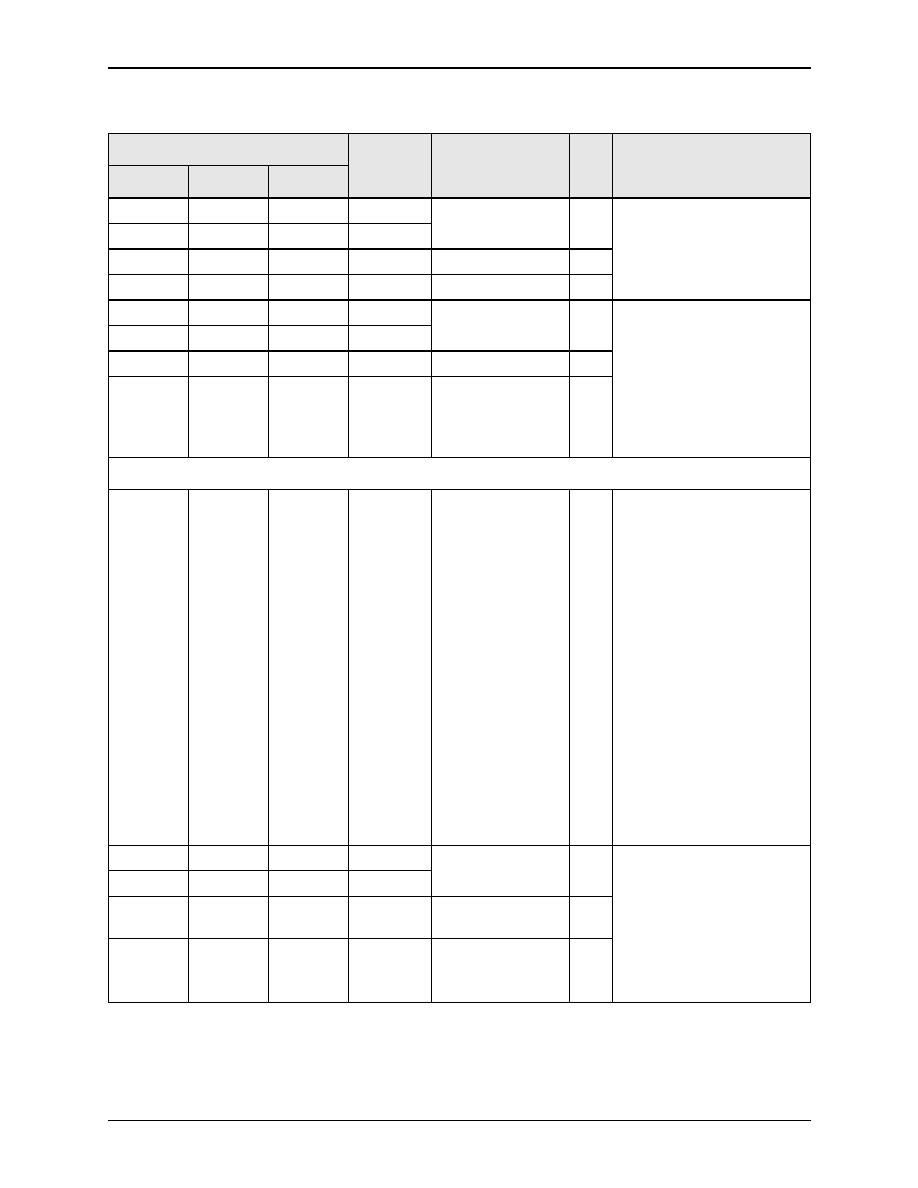
NOTE(S): The TX Monitor is only used with the 100-pin CX2833i-3X.
TPOS
TNEG
TCLK
ENCODER
TAIS
Pulse
Shaper
E3MODE
LINE
DRIVER
PDB
DATA
MUX
RLOOP
ENDECDIS
LLOOP
LBO
XOE
TLINEP
TLINEM/N
DECODER
RPOS
RNEG
RCLK
RLOS
TCLK
Clock/
Data
Recovery
PDATA
PDATA/
NDATA
NDATA
DATCLK
P
N
Receiver
TX
Monitor
ALOS
RLINEP
RLINEM/N
TMONP
TMONM
TXMON
TMONTST
REFCLK
REQH
LIU #1
LIU #2
LIU #3
CX28331/CX28332/CX28333
Single/Dual/Triple E3/DS3/STS-1 Line Interface Unit
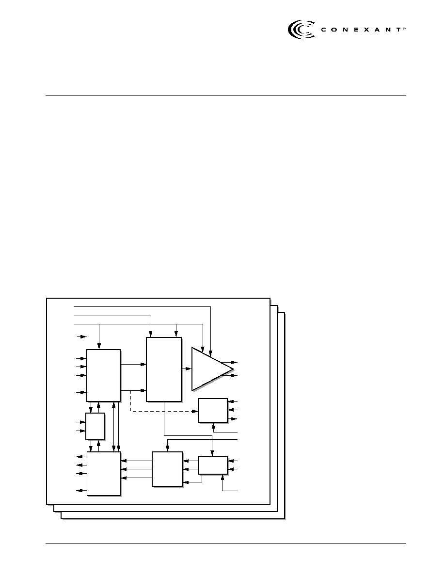
The CX28333 is a three-channel, E3/DS3/STS-1 fully-integrated Line Interface Unit
(LIU). It is configured via external pins and does not need a microprocessor interface.
Each channel has an independent equalizer on the receive side requiring no user
configuration. Also, each channel has a programmable transmit pulse shaper that can
be set to ensure that the cross-connect pulse mask requirement is met for transmit
cable length up to 450 feet. The CX28332 is a dual-channel, and the CX28331 is a
single-channel LIU with performance identical to the CX28333.
The CX28333 gives the user new economies of scale in concentrator applications
where three DS3 or STS-1 channels are concentrated into a single STS-3 channel. By
including three independent transceivers on a chip, significant external components are
eliminated, with the exception of 1:1 coupling transformers, termination resistors, and
supply bypass capacitors.
NOTE:
In this document, "i" is used to represent the number of channels:
i = 1 (CX28331), i = 2 (CX28332), and i = 3 (CX28333).
Functional Block Diagram
Distinguishing Features
∑
Can be used as a data transceiver
over a maximum of 900 feet of Type
734/728 coaxial cable or equivalent
in an on-premise environment
∑
Programmable pulse filtering to meet
cross-connect pulse masks (ANSI
T1.102-1993)
∑
Meets jitter specifications of Bellcore
GR499, GR253, and TBR24 (with
external JAT).
∑
Large input dynamic range
∑
Alarms for coding violation and loss
of signal
∑
Full diagnostic loopback capability
∑
Uses a minimum of external
components
∑
Compatible with ITU-T G.703, G.823
∑
Independent power down mode per
channel
∑
Easily interfaced to the DS3/E3
Framer IC (CX28342/3/4/6/8 and
CN8330)
∑
Selectable B3ZS/HDB3
encoding/decoding
∑
Superior input receiver sensitivity
(< 25 mV)
∑
Transmit monitor inputs (CX2833i-3x
series only)
Physical Characteristics
∑
80- and 100-pin ETQFP package
∑
Single 3.3 V power supply
∑
1 W maximum power dissipation
(CX28333)
∑
≠40 ∞C to +85 ∞C temperature range
∑
5 V-tolerant pins
∑
TTL digital pins
Applications
∑
Digital Cross-Connect Systems
∑
Routers
∑
ATM Switches
∑
Channelized Line Aggregation Units
∑
Test Equipment
∑
Channel Service Units
∑
Multiplexers
100985A
Conexant
© 2000,
Conexant Systems, Inc.
All Rights Reserved.
Information in this document is provided in connection with Conexant Systems, Inc. ("Conexant") products. These materials are
provided by Conexant as a service to its customers and may be used for informational purposes only. Conexant assumes no
responsibility for errors or omissions in these materials. Conexant may make changes to specifications and product descriptions at
any time, without notice. Conexant makes no commitment to update the information and shall have no responsibility whatsoever for
conflicts or incompatibilities arising from future changes to its specifications and product descriptions.
No license, express or implied, by estoppel or otherwise, to any intellectual property rights is granted by this document. Except as
provided in Conexant's Terms and Conditions of Sale for such products, Conexant assumes no liability whatsoever.
THESE MATERIALS ARE PROVIDED "AS IS" WITHOUT WARRANTY OF ANY KIND, EITHER EXPRESS OR IMPLIED, RELATING
TO SALE AND/OR USE OF CONEXANT PRODUCTS INCLUDING LIABILITY OR WARRANTIES RELATING TO FITNESS FOR A
PARTICULAR PURPOSE, CONSEQUENTIAL OR INCIDENTAL DAMAGES, MERCHANTABILITY, OR INFRINGEMENT OF ANY
PATENT, COPYRIGHT OR OTHER INTELLECTUAL PROPERTY RIGHT. CONEXANT FURTHER DOES NOT WARRANT THE
ACCURACY OR COMPLETENESS OF THE INFORMATION, TEXT, GRAPHICS OR OTHER ITEMS CONTAINED WITHIN THESE
MATERIALS. CONEXANT SHALL NOT BE LIABLE FOR ANY SPECIAL, INDIRECT, INCIDENTAL, OR CONSEQUENTIAL
DAMAGES, INCLUDING WITHOUT LIMITATION, LOST REVENUES OR LOST PROFITS, WHICH MAY RESULT FROM THE USE
OF THESE MATERIALS.
Conexant products are not intended for use in medical, lifesaving or life sustaining applications. Conexant customers using or selling
Conexant products for use in such applications do so at their own risk and agree to fully indemnify Conexant for any damages
resulting from such improper use or sale.
The following are trademarks of Conexant Systems, Inc.: ConexantTM, the Conexant C symbol, and "What's Next in Communications
Technologies"TM. Product names or services listed in this publication are for identification purposes only, and may be trademarks of
third parties. Third-party brands and names are the property of their respective owners.
For additional disclaimer information, please consult Conexant's Legal Information posted at
www.conexant.com
, which is
incorporated by reference.
Reader Response: Conexant strives to produce quality documentation and welcomes your feedback. Please send comments and
suggestions to
tech.pubs@conexant.com
. For technical questions, contact your local Conexant
sales office
or field applications
engineer.
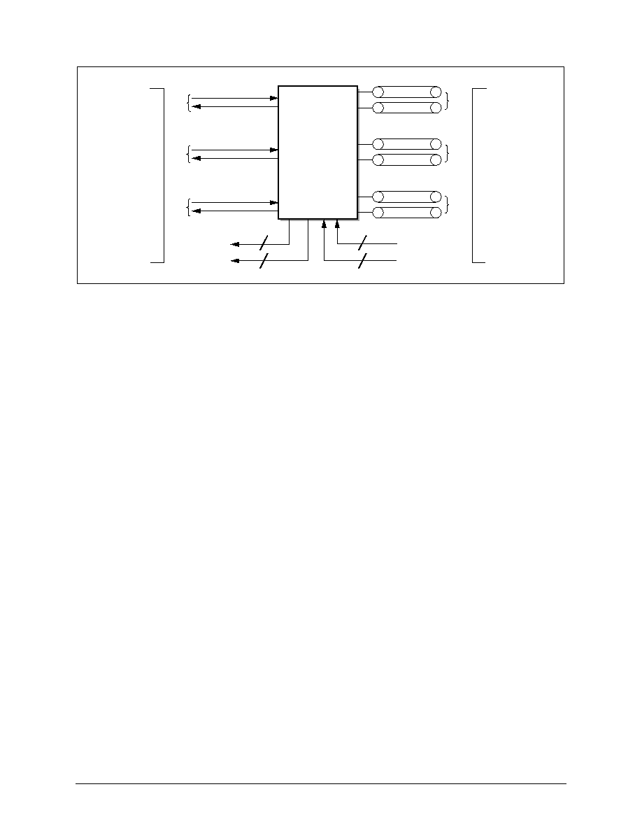
CX28333EVM
CH2
CH3
CX28333
NRZTX DATA and CLK in
Loss of Signal
Code Violation
Clock Input
Control
TX B3ZS/HDB3 analog out
RX B3ZS/HDB3 analog in
NRZRX DATA and CLK out
NRZTX DATA and CLK in
NRZRX DATA and CLK out
NRZTX DATA and CLK in
NRZRX DATA and CLK out
CH1
CH2
CH3
CH1
TX B3ZS/HDB3 analog out
RX B3ZS/HDB3 analog in
TX B3ZS/HDB3 analog out
RX B3ZS/HDB3 analog in
L
I
N
E
S
I
D
E
F
R
A
M
E
R
S
I
D
E
100985_002

100985A
Conexant
Ordering Information
Revision History
Model Number
Package
Description
Operating
Temperature
CX28331-1x
80-Pin ETQFP
Single-channel LIU
≠
40 ∞C to +85 ∞C
CX28332-1x
80-Pin ETQFP
Dual-channel LIU
≠
40 ∞C to +85 ∞C
CX28333-1x
80-Pin ETQFP
Triple-channel LIU
≠
40 ∞C to +85 ∞C
CX28331-3x
100-Pin ETQFP
Single channel with Transmit Monitoring
≠
40 ∞C to +85 ∞C
CX28332-3x
100-Pin ETQFP
Dual channel with Transmit Monitoring
≠
40 ∞C to +85 ∞C
CX28333-3x
100-Pin ETQFP
Triple channel with Transmit Monitoring
≠
40 ∞C to +85 ∞C
Revision
Level
Date
Description
A
--
May 5, 2000
Initial Release

100985A
Conexant

100985A
Conexant
v
Table of Contents
List of Figures
. . . . . . . . . . . . . . . . . . . . . . . . . . . . . . . . . . . . . . . . . . . . . . . . . . . . . . . . . . . . . . . . . . . . . . . . vii
List of Tables
. . . . . . . . . . . . . . . . . . . . . . . . . . . . . . . . . . . . . . . . . . . . . . . . . . . . . . . . . . . . . . . . . . . . . . . . . . ix
1.0
Pin Description
. . . . . . . . . . . . . . . . . . . . . . . . . . . . . . . . . . . . . . . . . . . . . . . . . . . . . . . . . . . . . . . . . 1-1
1.1
Pin Assignments
. . . . . . . . . . . . . . . . . . . . . . . . . . . . . . . . . . . . . . . . . . . . . . . . . . . . . . . . . . . . 1-1
2.0
Functional Description
. . . . . . . . . . . . . . . . . . . . . . . . . . . . . . . . . . . . . . . . . . . . . . . . . . . . . . . . . . 2-1
2.1
Overview
. . . . . . . . . . . . . . . . . . . . . . . . . . . . . . . . . . . . . . . . . . . . . . . . . . . . . . . . . . . . . . . . . . 2-1
2.2
Transmitter
. . . . . . . . . . . . . . . . . . . . . . . . . . . . . . . . . . . . . . . . . . . . . . . . . . . . . . . . . . . . . . . . 2-3
2.2.1
AMI B3ZS/HDB3 Encoder
. . . . . . . . . . . . . . . . . . . . . . . . . . . . . . . . . . . . . . . . . . . . . . . . 2-3
2.2.2
Pulse Shaper
. . . . . . . . . . . . . . . . . . . . . . . . . . . . . . . . . . . . . . . . . . . . . . . . . . . . . . . . . 2-3
2.2.3
Line Driver
. . . . . . . . . . . . . . . . . . . . . . . . . . . . . . . . . . . . . . . . . . . . . . . . . . . . . . . . . . . 2-4
2.2.3.1
Transmit Pulse Mask Templates
. . . . . . . . . . . . . . . . . . . . . . . . . . . . . . . . . . . 2-5
2.2.4
Alarm Indication Signal (AIS) Generator
. . . . . . . . . . . . . . . . . . . . . . . . . . . . . . . . . . . . . 2-8
2.2.5
Transmit Monitor Block (CX2833i-3x Only)
. . . . . . . . . . . . . . . . . . . . . . . . . . . . . . . . . . . 2-8
2.2.6
Jitter Generation (Intrinsic)
. . . . . . . . . . . . . . . . . . . . . . . . . . . . . . . . . . . . . . . . . . . . . . . 2-9
2.3
Receiver
. . . . . . . . . . . . . . . . . . . . . . . . . . . . . . . . . . . . . . . . . . . . . . . . . . . . . . . . . . . . . . . . . 2-10
2.3.1
Receive Sensitivity
. . . . . . . . . . . . . . . . . . . . . . . . . . . . . . . . . . . . . . . . . . . . . . . . . . . . 2-10
2.3.2
AGC/VGA Block
. . . . . . . . . . . . . . . . . . . . . . . . . . . . . . . . . . . . . . . . . . . . . . . . . . . . . . 2-10
2.3.3
Receive Equalizer
. . . . . . . . . . . . . . . . . . . . . . . . . . . . . . . . . . . . . . . . . . . . . . . . . . . . . 2-10
2.3.4
The PLL Clock Recovery Circuit
. . . . . . . . . . . . . . . . . . . . . . . . . . . . . . . . . . . . . . . . . . 2-11
2.3.5
Loss Of Signal (LOS) Detector
. . . . . . . . . . . . . . . . . . . . . . . . . . . . . . . . . . . . . . . . . . . 2-11
2.3.6
B3ZS/HDB3 Decoder With Bipolar Violation Detector
. . . . . . . . . . . . . . . . . . . . . . . . . . . 2-11
2.3.7
Data Squelching
. . . . . . . . . . . . . . . . . . . . . . . . . . . . . . . . . . . . . . . . . . . . . . . . . . . . . . 2-12
2.4
Jitter Tolerance
. . . . . . . . . . . . . . . . . . . . . . . . . . . . . . . . . . . . . . . . . . . . . . . . . . . . . . . . . . . . 2-13
2.4.1
Jitter Transfer
. . . . . . . . . . . . . . . . . . . . . . . . . . . . . . . . . . . . . . . . . . . . . . . . . . . . . . . . 2-15
2.5
Additional CX28331/CX28332/CX28333 Functions
. . . . . . . . . . . . . . . . . . . . . . . . . . . . . . . . . . 2-16
2.5.1
Bias Generator
. . . . . . . . . . . . . . . . . . . . . . . . . . . . . . . . . . . . . . . . . . . . . . . . . . . . . . . 2-16
2.5.2
Power-On Reset (POR)
. . . . . . . . . . . . . . . . . . . . . . . . . . . . . . . . . . . . . . . . . . . . . . . . . 2-16
2.5.3
Loopback Multiplexers (MUXes)
. . . . . . . . . . . . . . . . . . . . . . . . . . . . . . . . . . . . . . . . . . 2-16
2.6
Mechanical Specifications
. . . . . . . . . . . . . . . . . . . . . . . . . . . . . . . . . . . . . . . . . . . . . . . . . . . 2-17
2.7
Electrical Characteristics
. . . . . . . . . . . . . . . . . . . . . . . . . . . . . . . . . . . . . . . . . . . . . . . . . . . . 2-19

Table of Contents
CX28331/CX28332/CX28333
Single/Dual/Triple E3/DS3/STS-1 Line Interface Unit
vi
Conexant
100985A
2.7.1
Absolute Maximum Ratings
. . . . . . . . . . . . . . . . . . . . . . . . . . . . . . . . . . . . . . . . . . . . . 2-19
2.7.2
Recommended Operating Conditions
. . . . . . . . . . . . . . . . . . . . . . . . . . . . . . . . . . . . . . 2-20
2.8
DC Characteristics
. . . . . . . . . . . . . . . . . . . . . . . . . . . . . . . . . . . . . . . . . . . . . . . . . . . . . . . . . 2-21
2.9
AC Characteristics
. . . . . . . . . . . . . . . . . . . . . . . . . . . . . . . . . . . . . . . . . . . . . . . . . . . . . . . . . . 2-22
3.0
Applications
. . . . . . . . . . . . . . . . . . . . . . . . . . . . . . . . . . . . . . . . . . . . . . . . . . . . . . . . . . . . . . . . . . . 3-1
3.1
PCB Design Considerations for CX28331/CX28332/CX28333
. . . . . . . . . . . . . . . . . . . . . . . . . . . 3-1
3.1.1
Power Supply and Ground Plane
. . . . . . . . . . . . . . . . . . . . . . . . . . . . . . . . . . . . . . . . . . . 3-1
3.1.2
Impedance Matching
. . . . . . . . . . . . . . . . . . . . . . . . . . . . . . . . . . . . . . . . . . . . . . . . . . . 3-2
3.1.3
Other Passive Parts
. . . . . . . . . . . . . . . . . . . . . . . . . . . . . . . . . . . . . . . . . . . . . . . . . . . . 3-2
3.1.4
IBIS Models
. . . . . . . . . . . . . . . . . . . . . . . . . . . . . . . . . . . . . . . . . . . . . . . . . . . . . . . . . . 3-2
3.1.5
Recommended Vendors
. . . . . . . . . . . . . . . . . . . . . . . . . . . . . . . . . . . . . . . . . . . . . . . . . 3-2
Appendix A
. . . . . . . . . . . . . . . . . . . . . . . . . . . . . . . . . . . . . . . . . . . . . . . . . . . . . . . . . . . . . . . . . . . . . . . . . . A-1
A.1
Applicable Standards
. . . . . . . . . . . . . . . . . . . . . . . . . . . . . . . . . . . . . . . . . . . . . . . . . . . . . . . . A-1
Appendix B
. . . . . . . . . . . . . . . . . . . . . . . . . . . . . . . . . . . . . . . . . . . . . . . . . . . . . . . . . . . . . . . . . . . . . . . . . . B-1
B.1
Evaluation Module Schematic
. . . . . . . . . . . . . . . . . . . . . . . . . . . . . . . . . . . . . . . . . . . . . . . . . . B-1

CX28331/CX28332/CX28333
List of Figures
Single/Dual/Triple E3/DS3/STS-1 Line Interface Unit
100985A
Conexant
vii
List of Figures
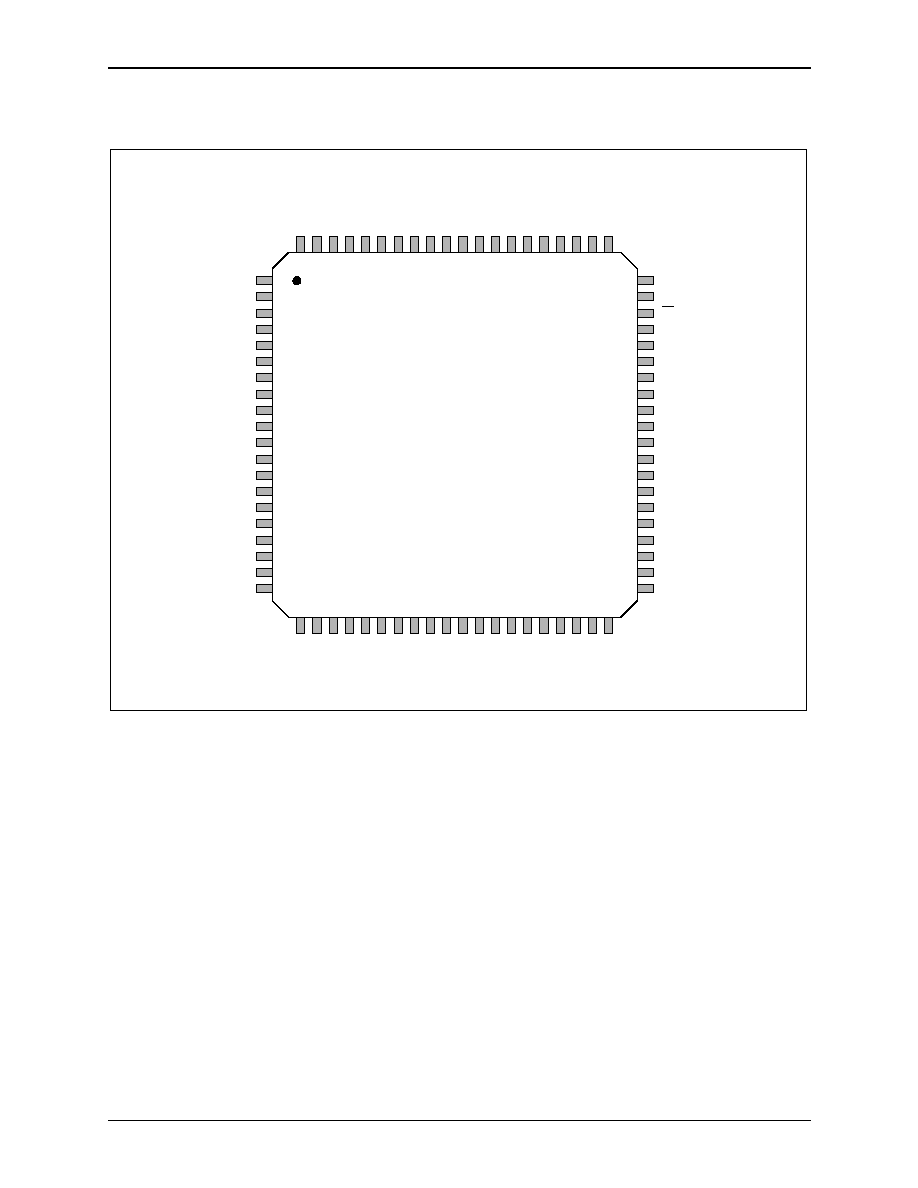
Figure 1-1.
CX28331-1x Pin Diagram . . . . . . . . . . . . . . . . . . . . . . . . . . . . . . . . . . . . . . . . . . . . . . . . . . 1-2
Figure 1-2.
CX28332-1x Pin Diagram . . . . . . . . . . . . . . . . . . . . . . . . . . . . . . . . . . . . . . . . . . . . . . . . . . 1-3
Figure 1-3.
CX28333-1x Pin Diagram . . . . . . . . . . . . . . . . . . . . . . . . . . . . . . . . . . . . . . . . . . . . . . . . . . 1-4
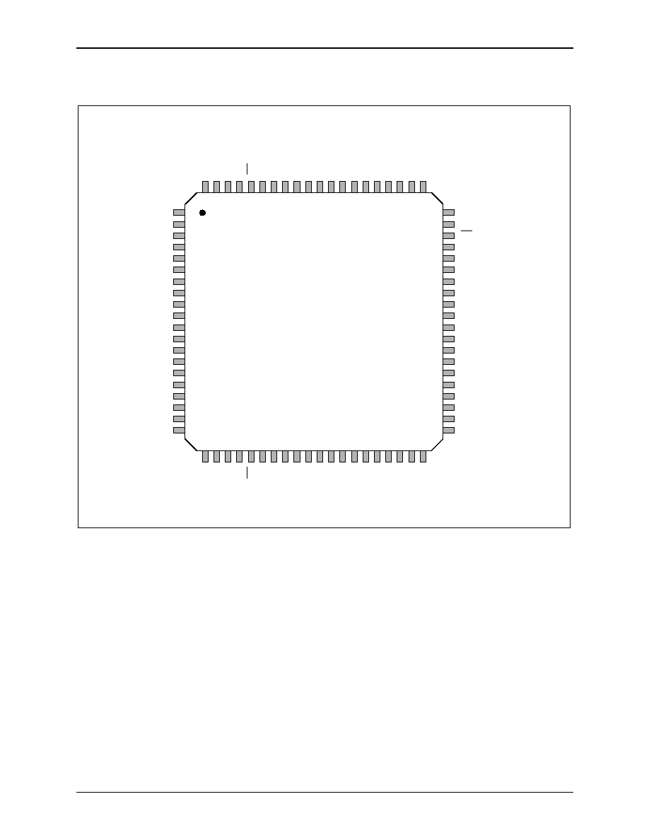
Figure 1-4.
CX28331-3x Pin Diagram . . . . . . . . . . . . . . . . . . . . . . . . . . . . . . . . . . . . . . . . . . . . . . . . . 1-11
Figure 1-5.
CX28332-3x Pin Diagram . . . . . . . . . . . . . . . . . . . . . . . . . . . . . . . . . . . . . . . . . . . . . . . . . 1-12
Figure 1-6.
CX28333-3x Pin Diagram . . . . . . . . . . . . . . . . . . . . . . . . . . . . . . . . . . . . . . . . . . . . . . . . . 1-13
Figure 2-1.
Typical Application Of Single CX2833i Channel . . . . . . . . . . . . . . . . . . . . . . . . . . . . . . . . . . 2-2
Figure 2-2.
Pulse Shaper . . . . . . . . . . . . . . . . . . . . . . . . . . . . . . . . . . . . . . . . . . . . . . . . . . . . . . . . . . . . 2-3
Figure 2-3.
Pulse Measurement Points . . . . . . . . . . . . . . . . . . . . . . . . . . . . . . . . . . . . . . . . . . . . . . . . . 2-4
Figure 2-4.
Transmit Pulse Mask for DS3 Rates . . . . . . . . . . . . . . . . . . . . . . . . . . . . . . . . . . . . . . . . . . 2-5
Figure 2-5.
Transmit Pulse Mask for STS-1 Rates . . . . . . . . . . . . . . . . . . . . . . . . . . . . . . . . . . . . . . . . . 2-6
Figure 2-6.
Transmit Pulse Mask for E3 Rate. . . . . . . . . . . . . . . . . . . . . . . . . . . . . . . . . . . . . . . . . . . . . 2-7
Figure 2-7.
AIS Signal . . . . . . . . . . . . . . . . . . . . . . . . . . . . . . . . . . . . . . . . . . . . . . . . . . . . . . . . . . . . . . 2-8
Figure 2-8.
Minimum Jitter Tolerance Requirement. . . . . . . . . . . . . . . . . . . . . . . . . . . . . . . . . . . . . . . 2-14
Figure 2-9.
Maximum Jitter Transfer Curve Requirement . . . . . . . . . . . . . . . . . . . . . . . . . . . . . . . . . . 2-15
Figure 2-10.
CX2833i-1x Mechanical Drawing (80-Pin)--Dimensions . . . . . . . . . . . . . . . . . . . . . . . . . 2-17
Figure 2-11.
CX2833i-3x Mechanical Drawing (100-Pin)--Dimensions . . . . . . . . . . . . . . . . . . . . . . . . 2-18
Figure 2-12.
Timing Diagram. . . . . . . . . . . . . . . . . . . . . . . . . . . . . . . . . . . . . . . . . . . . . . . . . . . . . . . . . 2-23
Figure 3-1.
Typical CX28333 Connection. . . . . . . . . . . . . . . . . . . . . . . . . . . . . . . . . . . . . . . . . . . . . . . . 3-3
Figure B-1.
Recommended Schematic for the CX2833i-1x Device . . . . . . . . . . . . . . . . . . . . . . . . . . . . B-2
Figure B-2.
Recommended Schematic for the CX2833i-3x Device (1 of 2) . . . . . . . . . . . . . . . . . . . . . . B-3
Figure B-3.
Recommended Schematic for the CX2833i-3x Device (2 of 2) . . . . . . . . . . . . . . . . . . . . . . B-4

List of Figures
CX28331/CX28332/CX28333
Single/Dual/Triple E3/DS3/STS-1 Line Interface Unit
viii
Conexant
100985A

CX28331/CX28332/CX28333
List of Tables
Single/Dual/Triple E3/DS3/STS-1 Line Interface Unit
100985A
Conexant
ix
List of Tables
Table 1-1.
CX28331/CX28332/CX28333 Pin Definitions . . . . . . . . . . . . . . . . . . . . . . . . . . . . . . . . . . . . 1-5
Table 1-2.
CX2833i-3x Pin Definitions . . . . . . . . . . . . . . . . . . . . . . . . . . . . . . . . . . . . . . . . . . . . . . . . . 1-14
Table 2-1.
DS3 Transmit Template Specifications . . . . . . . . . . . . . . . . . . . . . . . . . . . . . . . . . . . . . . . . . 2-5
Table 2-2.
STS-1 Transmit Template Specifications . . . . . . . . . . . . . . . . . . . . . . . . . . . . . . . . . . . . . . . . 2-6
Table 2-3.
Absolute Maximum Ratings . . . . . . . . . . . . . . . . . . . . . . . . . . . . . . . . . . . . . . . . . . . . . . . . 2-19
Table 2-4.
Recommended Operating Conditions . . . . . . . . . . . . . . . . . . . . . . . . . . . . . . . . . . . . . . . . . 2-20
Table 2-5.
DC Characteristics. . . . . . . . . . . . . . . . . . . . . . . . . . . . . . . . . . . . . . . . . . . . . . . . . . . . . . . . 2-21
Table 2-6.
AC Characteristics (Logic Timing) . . . . . . . . . . . . . . . . . . . . . . . . . . . . . . . . . . . . . . . . . . . . 2-22

List of Tables
CX28331/CX28332/CX28333
Single/Dual/Triple E3/DS3/STS-1 Line Interface Unit
x
Conexant
100985A

100985A
Conexant
1-1
1
1.0 Pin Description
1.1 Pin Assignments
Figures 1-1
(CX28331-1x),
1-2
(CX28332-1x), and
1-3
(CX28333-1x) illustrate
pin assignments for the 80-pin Exposed Thin Quad Flat Package (ETQFP). See
Table 1-1
for the CX2833i-1x pin descriptions.
Figures 1-4
(CX28331-3x),
1-5
(CX28332-3x), and
1-6
(CX28333-3x)
illustrate pin assignments for the 100-pin ETQFP. The 100-pin package adds
more functionality, supporting new features such as Transmit Monitoring and
Transmit Monitoring Status testing. See
Table 1-2
for the CX2833i-3x pin
descriptions.
The input/output (I/O) column is coded as follows:
I = Input
O = Output
I/O = Bidirectional
P = Power
NOTE:
All digital inputs and outputs contain 75 k
pull-down resistors.
When a channel is disabled (i.e., the PDx pin is tied low or not connected), all
receive and transmit analog circuitry powers down. Analog inputs (RLINE) are
ignored and analog outputs (TLINE) are high impedance. Digital inputs of a
powered-down channel are still active, but ignored. Overall noise on the device
can be lowered by not driving the digital inputs of a powered-down channel.
NOTE:
When power is disconnected from the device, TLINE pins are low
impedance to ground if driven by more than one forward-bias diode
voltage (0.7 V) below ground. Additionally, driving TLINE, a
forward-bias diode voltage above the VGG pin, creates a low impedance
path from the TLINE pin to the VGG pin. Otherwise, the TLINE pins are
high impedance.
1.0 Pin Description
CX28331/CX28332/CX28333
1.1 Pin Assignments
Single/Dual/Triple E3/DS3/STS-1 Line Interface Unit
1-2
Conexant
100985A
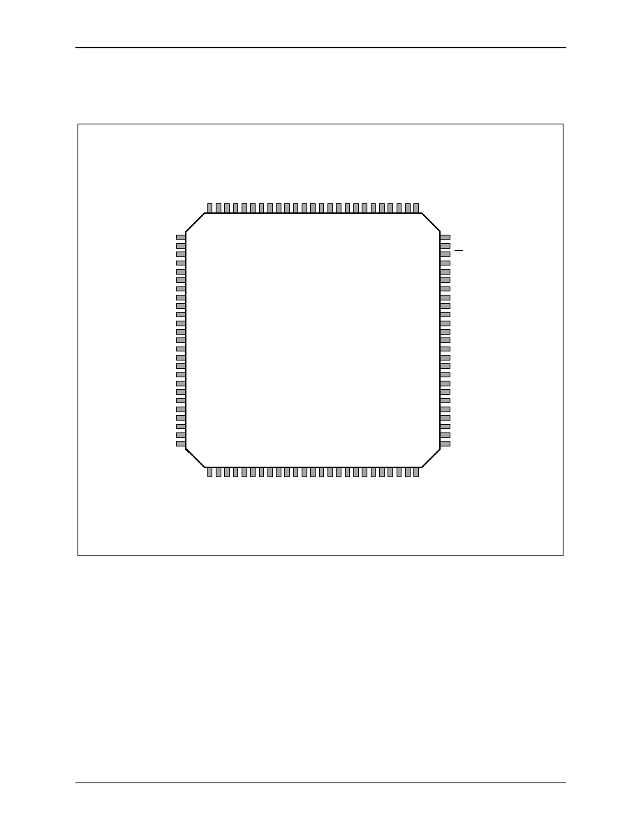
Figure 1-1. CX28331-1x Pin Diagram
CX28331-1x
76
77
78
79
80
NC
GPD
RESET
VGG
RBIAS
71
72
73
74
75
NC
NC
DVDDIO
NC
NC
66
67
68
69
70
NC
NC
NC
NC
NC
61
62
63
64
65
NC
NC
NC
NC
NC
56
57
58
59
60
L L O O P
R L O O P
PD
ENDECDIS
D V D D C
51
52
53
54
55
TAIS
R L O S
R C L K
RPOS/RNRZ
RNEG/RLCV
46
47
48
49
50
REQH
R E F C L K
T C L K
TPOS/TNRZ
TNEG/NC
41
42
43
44
45
DVSSC
N C
E 3 M O D E
L B O
XOE
5
4
3
2
1
10
9
8
7
6
15
14
13
12
11
20
19
18
17
16
25
24
23
22
21
NC
VSS
NC
NC
VDD
30
29
28
27
26
NC
NC
DVSSIO
NC
NC
35
34
33
32
31
NC
NC
NC
NC
NC
40
39
38
37
36
NC
NC
NC
NC
NC
RVSS
RLINEN
RLINEP
RVDD
V D D
NC
NC
VSS
TVDD
TLINEN
TLINEP
TVSS
VSS
V D D
NC
NC
VSS
NC
V D D
NC
100985_003

CX28331/CX28332/CX28333
1.0 Pin Description
Single/Dual/Triple E3/DS3/STS-1 Line Interface Unit
1.1 Pin Assignments
100985A
Conexant
1-3
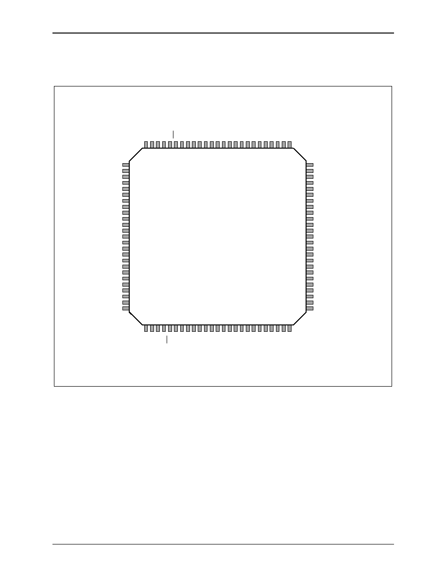
Figure 1-2. CX28332-1x Pin Diagram
CX28332-1x
76
77
78
79
80
PD1
GPD
RESET
VGG
RBIAS
71
72
73
74
75
XOE1
LBO1
DVDDIO
LLOOP1
RLOOP1
66
67
68
69
70
RLOS1
RCLK1
RPOS1/RNRZ1
RNEG1/RLCV1
REQH1
61
62
63
64
65
TAIS1
TCLK1
TPOS1/TNRZ1
TNEG1/NC1
REFCLK1
56
57
58
59
60
NC
NC
NC
NC
NC
NC
NC
NC
NC
NC
NC
NC
NC
NC
NC
E3MODE
ENDECDIS
D V D D C
51
52
53
54
55
46
47
48
49
50
41
42
43
44
45
DVSSC
N C
5
4
3
2
1
10
9
8
7
6
15
14
13
12
11
20
19
18
17
16
25
24
23
22
21
PD2
RVSS2
RLINE2N
RLINE2P
RVDD2
30
29
28
27
26
XOE2
LBO2
DVSSIO
LLOOP2
RLOOP2
35
34
33
32
31
RLOS2
RCLK2
RPOS2/RNRZ2
RNEG2/RLCV2
REQH2
40
39
38
37
36
TAIS2
TNEG2/NC2
TPOS2/TNRZ2
TCLK2
REFCLK2
T V D D 2
TLINE2N
TLINE2P
TVSS2
VSS
NC
NC
VDD
VDD
NC
NC
VSS
TVSS1
T V D D 1
TLINE1N
TLINE1P
RVSS1
RLINE1P
R V D D 1
RLINE1N
100985_004
1.0 Pin Description
CX28331/CX28332/CX28333
1.1 Pin Assignments
Single/Dual/Triple E3/DS3/STS-1 Line Interface Unit
1-4
Conexant
100985A
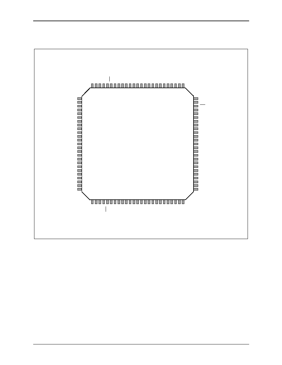
Figure 1-3. CX28333-1x Pin Diagram
CX28333-1x
76
77
78
79
80
PD1
GPD
RESET
VGG
RBIAS
71
72
73
74
75
XOE1
LBO1
DVDDIO
LLOOP1
RLOOP1
66
67
68
69
70
RLOS1
RCLK1
RPOS1/RNRZ1
RNEG1/RLCV1
REQH1
61
62
63
64
65
TAIS1
TCLK1
TPOS1/TNRZ1
TNEG1/NC1
REFCLK1
56
57
58
59
60
L L O O P 2
R L O O P 2
PD2
ENDECDIS
D V D D C
51
52
53
54
55
TAIS2
R L O S 2
R C L K 2
RPOS2/RNRZ2
RNEG2/RLCV2
46
47
48
49
50
REQH2
R E F C L K 2
T C L K 2
TPOS2/TNRZ2
TNEG2/NC2
41
42
43
44
45
DVSSC
E 3 M O D E
N C
L B O 2
XOE2
5
4
3
2
1
10
9
8
7
6
15
14
13
12
11
20
19
18
17
16
25
24
23
22
21
PD3
RVSS3
RLINE3N
RLINE3P
RVDD3
30
29
28
27
26
XOE3
LBO3
DVSSIO
LLOOP3
RLOOP3
35
34
33
32
31
RLOS3
RCLK3
RPOS3/RNRZ3
RNEG3/RLCV3
REQH3
40
39
38
37
36
TAIS3
TNEG3/NC3
TPOS3/TNRZ3
TCLK3
REFCLK3
RVSS2
RLINE2N
RLINE2P
R V D D 2
T V D D 3
TLINE3N
TLINE3P
TVSS3
T V D D 2
TLINE2N
TLINE2P
TVSS2
TVSS1
T V D D 1
TLINE1N
TLINE1P
RVSS1
RLINE1P
R V D D 1
RLINE1N
100985_005

CX28331/CX28332/CX28333
1.0 Pin Description
Single/Dual/Triple E3/DS3/STS-1 Line Interface Unit
1.1 Pin Assignments
100985A
Conexant
1-5
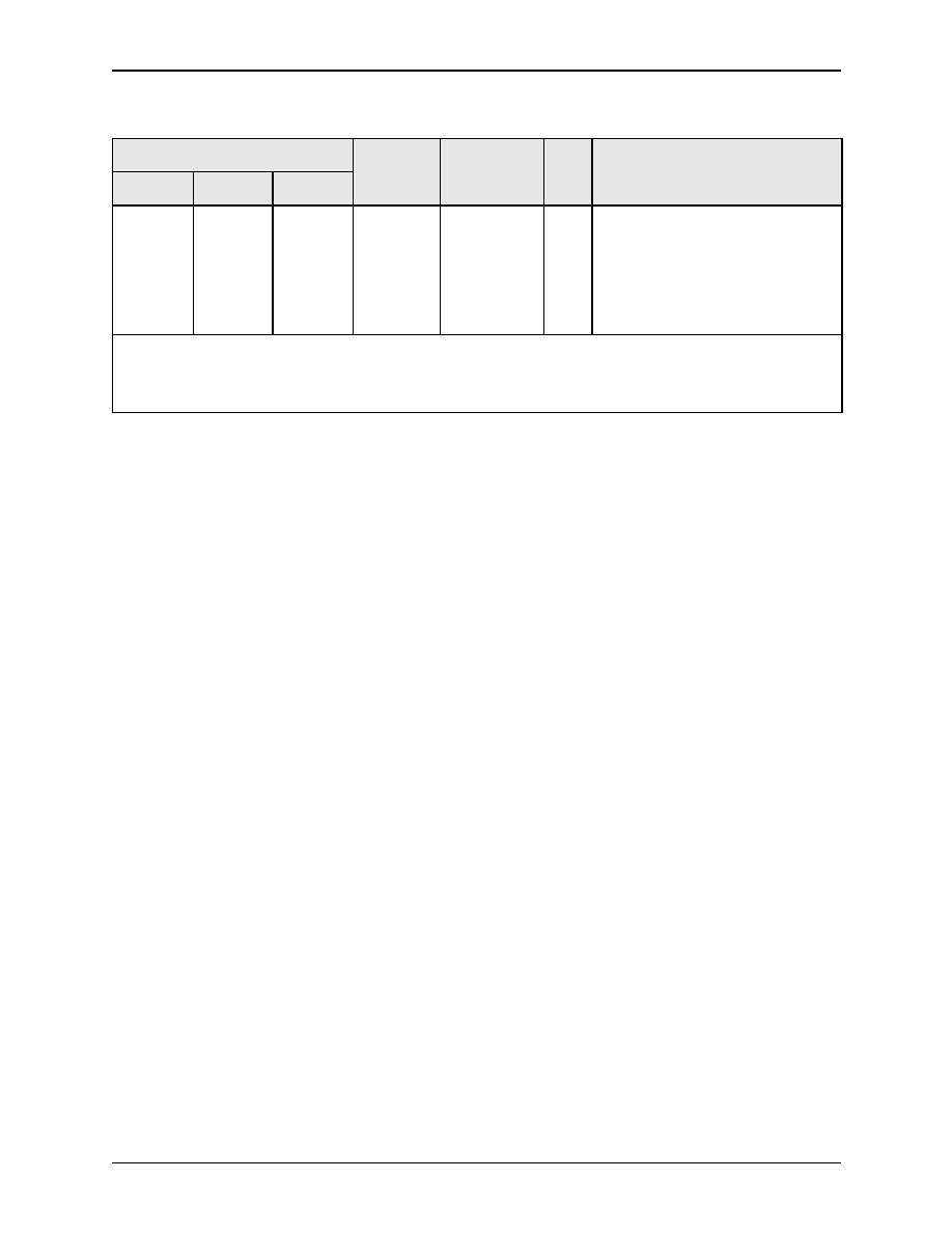
Table 1-1. CX2833i-1x Pin Definitions (1 of 6)
Pin #
Signal Name
Description
I/O/P
Notes
CX28331-1x CX28332-1x CX28333-1x
Coaxial Line Pins
14
--
--
RLINEP
Ch1 positive receive
data
I
Differential inputs for each channel
from its respective receive coax
line. The RX expects balanced
differential inputs, usually achieved
using a 1:1 transformer.
The inputs are internally DC biased
to 1.9 V.
--
6
6
RLINE1P
15
--
--
RLINEN
Ch1 negative receive
data
I
--
7
7
RLINE1N
--
22
14
RLINE2P
Ch2 positive receive
data
I
--
23
15
RLINE2N
Ch2 negative receive
data
I
--
--
22
RLINE3P
Ch3 positive receive
data
I
--
--
23
RLINE3N
Ch3 negative receive
data
I
10
--
--
TLINEP Ch1
positive
transmit
data
O
Differential, coax-driver balanced
outputs for pulse-shaped AMI
B3ZS/HDB3 encoded waveforms
for each channel.
These pins should be connected to
the primary side of the 1:1
transformer through two
backmatch resistors (see
Appendix
B
).
--
2
2
TLINE1P
11
--
--
TLINEN Ch1
negative
transmit
data
O
--
3
3
TLINE1N
--
18
10
TLINE2P
Ch2 positive transmit
data
O
--
19
11
TLINE2N
Ch2 negative transmit
data
O
--
--
18
TLINE3P
Ch3 positive transmit
data
O
--
--
19
TLINE3N
Ch3 negative transmit
data
O

1.0 Pin Description
CX28331/CX28332/CX28333
1.1 Pin Assignments
Single/Dual/Triple E3/DS3/STS-1 Line Interface Unit
1-6
Conexant
100985A
Digital Data Pins
54
--
--
RPOS/
RNRZ
Ch1 receive Positive rail
or NRZ data
O
Resynchronized receive data
intended to be strobed out by the
corresponding RCLK.
When ENDECDIS = 1, these outputs
are positive and negative AMI data
(RPOS and RNEG).
When ENDECDIS = 0, these outputs
are decoded NRZ data (RNRZ) and
line code violation (RLCV). A line
code violation is indicated when
RLCV = 1.
See notes on the ENDECDIS pin in
the Control Signals section.
--
68
68
RPOS1/
RNRZ1
55
--
--
RNEG/
RLCV
Ch1 receive Negative rail
or line code violation
O
--
69
69
RNEG1/
RLCV1
--
33
54
RPOS2/
RNRZ2
Ch2 receive Positive rail
or NRZ data
O
--
32
55
RNEG2/
RLCV2
Ch2 receive Negative rail
or line code violation
O
--
--
33
RPOS3/
RNRZ3
Ch3 receive Positive rail
or NRZ data
O
--
--
32
RNEG3/
RLCV3
Ch3 receive Negative rail
or line code violation
O
53
--
--
RCLK
Receive clock Ch1
O
Recovered clock for each channel
receiver, intended for strobing the
corresponding RDAT into the
following framer or logic.
--
67
67
RCLK1
--
34
53
RCLK2
Receive clock Ch2
O
--
--
34
RCLK3
Receive clock Ch3
O
49
--
--
TPOS/
TNRZ
Ch1 transmit Positive
rail or NRZ data
I
Synchronized transmit data
intended to be strobed in by the
corresponding TCLK.
When ENDECDIS = 1, these inputs
are expected to be positive and
negative AMI data (TPOS and
TNEG).
When ENDECDIS = 0, these inputs
are expected to be uncoded NRZ
data (TNRZ) and no connects (NC).
See notes on the ENDECDIS pin in
the Control Signals section.
--
63
63
TPOS1/
TNRZ1
48
--
--
TNEG/
NC
Ch1 transmit Negative
rail or no connect data
I
--
64
64
TNEG1/
NC1
--
38
49
TPOS2/
TNRZ2
Ch2 transmit Positive or
NRZ data
I
--
37
48
TNEG2/
NC2
Ch2 transmit Negative
rail or no connect data
I
--
--
38
TPOS3/
TNRZ3
Ch3 transmit Positive or
NRZ data
I
--
--
37
TNEG3/
NC3
Ch3 transmit Negative
rail or no connect data
I
Table 1-1. CX2833i-1x Pin Definitions (2 of 6)
Pin #
Signal Name
Description
I/O/P
Notes
CX28331-1x CX28332-1x CX28333-1x
CX28331/CX28332/CX28333
1.0 Pin Description
Single/Dual/Triple E3/DS3/STS-1 Line Interface Unit
1.1 Pin Assignments
100985A
Conexant
1-7
50
--
--
TCLK
Transmit clock Ch1
I
Transmit bit clock input for strobing
with transmit data into the CX2833i.
--
62
62
TCLK1
--
39
50
TCLK2
Transmit clock Ch2
I
--
--
39
TCLK3
Transmit clock Ch3
I
52
--
--
RLOS
Loss of signal Ch1
O
Loss Of Signal (LOS) indication for
each channel, as determined by
insufficient pulse density. Signal
loss detected when RLOS = 1. An
LOS will be asserted when 175 ±75
0s occur in a row and deasserted
when the pulse density is between
28% and 33% (DS3/STS-1) (i.e., a
1s density).
--
66
66
RLOS1
--
35
52
RLOS2
Loss of signal Ch2
O
--
--
35
RLOS3
Loss of signal Ch3
O
Control Signals
59
59
59
ENDECDIS
Encoder/decoder
disable (for all channels)
I
1 = Dual rail pulse coded data
format. Input transmit data pins
TPOS, TNRZ, TNEG and NC are
interpreted as TPOS and TNEG
(encoded positive and negative rail
data). Output receive data pins
RPOS and RNRZ, and RNEG and
RLCV are interpreted as RPOS and
RNEG, with RPOS having a positive
pulse in place of every positive AMI
pulse and RNEG having a negative
pulse in place of every negative AMI
pulse.
0 = NRZ format. Transmit data pins
TPOS and TNEG are interpreted as
TNRZ and NC (not connected).
Receive data pins RPOS and RNEG
are interpreted as RNRZ and RLCV.
In this mode, all line code violations
are reported as active high on
RLCV.
51
--
--
TAIS
Transmit Ch1 AIS mode
enable
I
Transmission of Alarm Indication
Signal (AIS) for a given channel.
Replace transmit data with AIS
signal. The AMI form of AIS
supported is alternating 1s.
(+1, -1, +1, -1, +1, ...)
Looping takes precedence over AIS.
1 = AIS mode enabled
0 = AIS mode disabled
--
61
61
TAIS1
--
40
51
TAIS2
Transmit Ch2 AIS mode
enable
I
--
--
40
TAIS3
Transmit Ch3 AIS mode
enable
I
Table 1-1. CX2833i-1x Pin Definitions (3 of 6)
Pin #
Signal Name
Description
I/O/P
Notes
CX28331-1x CX28332-1x CX28333-1x

1.0 Pin Description
CX28331/CX28332/CX28333
1.1 Pin Assignments
Single/Dual/Triple E3/DS3/STS-1 Line Interface Unit
1-8
Conexant
100985A
43
43
43
E3MODE
E3MODE
I
When the pin is set to high, it
enables the E3 mode on all
channels, instead of the DS3/STS-1
mode. This also changes the pulse
shaper to E3 mode and overrides all
LBO pins. It also changes the
encoder/decoder from B3ZS mode
to HDB3 mode.
1 = E3 mode
0 = DS3/STS-1 mode
44
--
--
LBO
Transmit line Ch1
build-out mode
I
Line build-out mode per channel,
based on the length of cable on the
transmit side of the cross-connect
block. This bit is overridden and the
pulse shaper is disabled (no pulse
shaping) if E3MODE = 1.
1 = Inserts line build-out into the
transmit channel. Usually used
when the transmit cable is less than
350 feet in length.
0 = Line build-out bypassed (not
inserted). Usually used when the
transmit cable is greater than 350
feet in length.
--
72
72
LBO1
--
29
44
LBO2
Transmit line Ch2
build-out mode
I
--
--
29
LBO3
Transmit line Ch3
build-out mode
I
56
--
--
LLOOP
Local loopback enable
Ch1
I
Local loopback enable per channel.
The transmit data is looped back
immediately from the encoder to
the decoder in place of the received
data.
1 = local loopback enabled
0 = local loopback disabled
--
74
74
LLOOP1
--
27
56
LLOOP2
Local loopback enable
Ch2
I
--
--
27
LLOOP3
Local loopback enable
Ch3
I
57
--
--
RLOOP
Remote loopback enable
Ch1
I
Remote loopback enable per
channel. The receive data, retimed
after clock recovery, is looped back
into the AMI generator in place of
the transmit data.
1 = remote loopback enabled
0 = remote loopback disabled
--
75
75
RLOOP1
--
26
57
RLOOP2
Remote loopback enable
Ch2
I
--
--
26
RLOOP3
Remote loopback enable
Ch3
I
45
--
--
XOE
Transmit output enable
Ch1
I
Transmit output enable per channel.
1 = transmit line output driver
enabled
0 = transmit output driver set to
high impedance state
--
71
71
XOE1
--
30
45
XOE2
Transmit output enable
Ch2
I
--
--
30
XOE3
Transmit output enable
Ch3
I
Table 1-1. CX2833i-1x Pin Definitions (4 of 6)
Pin #
Signal Name
Description
I/O/P
Notes
CX28331-1x CX28332-1x CX28333-1x

CX28331/CX28332/CX28333
1.0 Pin Description
Single/Dual/Triple E3/DS3/STS-1 Line Interface Unit
1.1 Pin Assignments
100985A
Conexant
1-9
46
--
--
REQH
Ch1 Receive High EQ
Gain Enable
I
The equalizer in the CX2833i has
two gain settings. The higher gain
setting is designed to optimally
equalize a nominally-shaped (meets
the pulse template), pulse-driven
DS3 or STS-1 waveform that is
driven through 0≠900 feet of cable.
Square-shaped pulses such as E3
or DS3-HIGH require less
high-frequency gain and should use
the low EQ gain setting.
REQH = 1 high EQ gain
(DS3/STS-1 modes)
REQH = 0 low EQ gain (E3/DS3
Square Modes)
--
70
70
REQH1
--
31
46
REQH2
Ch2 Receive High EQ
Gain Enable
--
--
31
REQH3
Ch3 Receive High EQ
Gain Enable
I
Power/Ground
12
--
--
TVDD
TX power Ch1
P
Power pins for transmit circuitry
per channel (3.3 V).
--
4
4
TVDD1
--
20
12
TVDD2
TX power Ch2
P
--
--
20
TVDD3
TX power Ch3
P
9
--
--
TVSS
TX ground Ch1
P
Ground pins for transmit circuitry
per channel.
--
1
1
TVSS1
--
17
9
TVSS2
TX ground Ch2
P
--
--
17
TVSS3
TX ground Ch3
P
13
--
--
RVDD
RX power Ch1
P
Power pins for receive circuitry per
channel (3.3 V).
Connect to 3.3 V power.
--
5
5
RVDD1
--
21
13
RVDD2
RX power Ch2
P
--
--
21
RVDD3
RX power Ch3
P
16
--
--
RVSS
RX ground Ch1
P
Ground pins for receive circuitry
per channel.
Connect to ground.
--
8
8
RVSS1
--
24
16
RVSS2
RX ground Ch2
P
--
--
24
RVSS3
RX ground Ch3
P
60
60
60
DVDDC
Digital core power
P
Digital core power for all channels
(3.3 V).
41
41
41
DVSSC
Digital core ground
P
Digital core ground for all channels.
79
79
79
VGG
5 V/3.3 V ESD pin
(1)
P
5 V supply for 5 V-tolerant, digital
pad ESD diodes. No static power is
drawn from pin.
73
73
73
DVDDIO
Digital I/O power
P
Connect to 3.3 V digital power.
28
28
28
DVSSIO
Digital ground
P
Digital ground.
Table 1-1. CX2833i-1x Pin Definitions (5 of 6)
Pin #
Signal Name
Description
I/O/P
Notes
CX28331-1x CX28332-1x CX28333-1x

1.0 Pin Description
CX28331/CX28332/CX28333
1.1 Pin Assignments
Single/Dual/Triple E3/DS3/STS-1 Line Interface Unit
1-10
Conexant
100985A
4, 5, 20, 21
12, 13
--
VDD
Power
P
Connect to 3.3 V power.
1, 8, 17, 24
9, 16
--
VSS
Ground
P
Connect to ground.
Miscellaneous
58
--
--
PD
Power down for Ch1
I
Power down transceiver channel
0 = Power down channel (off)
1 = Channel active (on)
Note: A special power-down mode
exists when all three PDBs are set
low. This special mode shuts off the
entire chip (including biasing). This
is useful for static Idd testing.
--
76
76
PD1
--
25
58
PD2
Power down for Ch2
I
--
--
25
PD3
Power down for Ch3
I
47
--
--
REFCLK
Reference clock for Ch1
I
Reference clock from off-chip.
This clock should be set to one of
the following:
∑
E3 rate (34.368 MHz)
∑
DS3 rate (44.736 MHz)
∑
STS-1 rate (51.84 MHz)
The clock rate should correspond to
the mode of operation that has been
chosen for the channel.
--
65
65
REFCLK1
--
36
47
REFCLK2
Reference clock for Ch2
I
--
--
36
REFCLK3
Reference clock for Ch3
I
80
80
80
RBIAS
Bias resistor
O
A 12.1 k
± 1% resistor tied from
this pin to ground provides the
current reference to the entire
chip.
(2)
78
78
78
Reset
Reset
I/O
Asynchronous reset (reset entire
device).
77
77
77
GPD
Global Power down
I/O
Power down (Static Idd testing).
0 = Power down disable
1 = Power down active
2, 3, 6, 7, 18,
19, 22, 23,
25, 26, 27,
29, 30, 31,
32, 33, 34,
35, 36, 37,
38, 39, 40,
42, 61, 62,
63, 64, 65,
66, 67, 68,
69, 70, 71,
72, 74, 75,
76
10, 11, 14,
15, 42,
44≠58
42
NC
No connect
--
Not connected.
NOTE(S):
(1)
This pin should be connected to 3.3 V in an all-3.3 V design.
(2)
Placing a capacitor from this pin to ground may result in instabilities.
3. All digital input pins contain a 75 k
pull-down resistor from input to DVSS.
Table 1-1. CX2833i-1x Pin Definitions (6 of 6)
Pin #
Signal Name
Description
I/O/P
Notes
CX28331-1x CX28332-1x CX28333-1x
CX28331/CX28332/CX28333
1.0 Pin Description
Single/Dual/Triple E3/DS3/STS-1 Line Interface Unit
1.1 Pin Assignments
100985A
Conexant
1-11
Figure 1-4. CX28331-3x Pin Diagram
100985_015
1
2
3
4
5
6
7
8
9
10
11
12
13
14
15
16
17
18
19
20
21
22
23
24
25
75
74
73
72
71
70
69
68
67
66
65
64
63
62
61
60
59
58
57
56
55
54
53
52
51
100
99
98
97
96
95
94
93
92
91
90
89
88
87
86
85
84
83
82
81
80
79
78
77
76
DVDDC
ENDECDIS
PD
RLOOP
LLOOP
RNEG/RLCV
RPOS/RNRZ
RCLK
RLOS
NC
NC
NC
TAIS
TCLK
TPOS/TNRZ
TNEG/NC
TLOS
REFCLK
REQH
XOE
LBO
TMONTST
E3MODE
NC
DVSSC
VSS
RBIAS
VGG
RESET
GPD
NC
NC
NC
DVDDIO
NC
NC
NC
NC
NC
NC
NC
NC
NC
NC
NC
NC
NC
NC
NC
NC
26
27
28
29
30
31
32
33
34
35
36
37
38
39
40
41
42
43
44
45
46
47
48
49
50
NC
NC
NC
NC
VDD
VDD
NC
NC
VSS
TVSS
TMONP
TLINEP
TLINEM
TMONM
TVDD
RVDD
RLINEP
RLINEM
RVSS
VSS
NC
NC
NC
NC
VDD
VDD
NC
NC
VSS
NC
NC
NC
DVSSIO
NC
NC
NC
NC
NC
NC
NC
NC
NC
NC
NC
NC
NC
NC
NC
NC
NC
CX28331-3x
1.0 Pin Description
CX28331/CX28332/CX28333
1.1 Pin Assignments
Single/Dual/Triple E3/DS3/STS-1 Line Interface Unit
1-12
Conexant
100985A
Figure 1-5. CX28332-3x Pin Diagram
100985_016
1
2
3
4
5
6
7
8
9
10
11
12
13
14
15
16
17
18
19
20
21
22
23
24
25
75
74
73
72
71
70
69
68
67
66
65
64
63
62
61
60
59
58
57
56
55
54
53
52
51
100
99
98
97
96
95
94
93
92
91
90
89
88
87
86
85
84
83
82
81
80
79
78
77
76
DVDDC
ENDECDIS
NC
NC
NC
NC
NC
NC
NC
NC
NC
NC
NC
NC
NC
NC
NC
NC
NC
NC
NC
TMONTST
E3MODE
NC
DVSSC
TVSS1
RBIAS
VGG
RESET
GPD
PD1
RLOOP1
LLOOP1
DVDDIO
LBO1
XOE1
REQH1
NC
NC
NC
RNEG1/RLCV1
RPOS1/RNRZ1
RCLK1
RLOS1
REFCLK1
TLOS1
TNEG1/NC1
TPOS1/TNRZ1
TCLK1
TAIS1
26
27
28
29
30
31
32
33
34
35
36
37
38
39
40
41
42
43
44
45
46
47
48
49
50
TMON1P
TLINE1P
TLINE1M
TMON1M
TVDD1
RVDD1
RLINE1P
RLINE1M
RVSS1
VSS
NC
NC
NC
NC
VDD
VDD
NC
NC
VSS
TVSS2
TMON2P
TLINE2P
TLINE2M
TMON2M
TVDD2
RVDD2
RLINE2P
RLINE2M
RVSS2
PD2
RLOOP2
LLOOP2
DVSSIO
LBO2
XOE2
REQH2
NC
NC
NC
RNEG2/RLCV2
RPOS2/RNRZ2
RCLK2
RLOS2
REFCLK2
TLOS2
TNEG2/NC2
TPOS2/TNRZ2
TCLK2
TAIS2
NC
CX28332-3x
CX28331/CX28332/CX28333
1.0 Pin Description
Single/Dual/Triple E3/DS3/STS-1 Line Interface Unit
1.1 Pin Assignments
100985A
Conexant
1-13
Figure 1-6. CX28333-3x Pin Diagram
100985_006
1
2
3
4
5
6
7
8
9
10
11
12
13
14
15
16
17
18
19
20
21
22
23
24
25
75
74
73
72
71
70
69
68
67
66
65
64
63
62
61
60
59
58
57
56
55
54
53
52
51
100
99
98
97
96
95
94
93
92
91
90
89
88
87
86
85
84
83
82
81
80
79
78
77
76
DVDDC
ENDECDIS
PD2
RLOOP2
LLOOP2
RNEG2 / RLCV2
RPOS2 / RNRZ2
RCLK2
RLOS2
NC
NC
NC
TAIS2
TCLK2
TPOS2/TNRZ2
TNEG2/NC2
TLOS2
REFCLK2
REQH2
XOE2
LBO2
TMONTST
E3MODE
NC
DVSSC
TVSS1
RBIAS
VGG
RESET
GPD
PD1
RLOOP1
LLOOP1
DVDDIO
LBO1
XOE1
REQH1
NC
NC
NC
RNEG1/RLCV1
RPOS1/RNRZ1
RCLK1
RLOS1
REFCLK1
TLOS1
TNEG1/NC1
TPOS1/TNRZ1
TCLK1
TAIS1
26
27
28
29
30
31
32
33
34
35
36
37
38
39
40
41
42
43
44
45
46
47
48
49
50
TMON1P
TLINE1P
TLINE1M
TMON1M
TVDD1
RVDD1
RLINE1P
RLINE1M
RVSS1
TVSS2
TMON2P
TLINE2P
TLINE2M
TMON2M
TVDD2
RVDD2
RLINE2P
RLINE2M
RVSS2
TVSS3
TMON3P
TLINE3P
TLINE3M
TMON3M
TVDD3
RVDD3
RLINE3P
RLINE3M
RVSS3
PD3
RLOOP3
LLOOP3
DVSSIO
LBO3
XOE3
REQH3
NC
NC
NC
RNEG3/RLCV3
RPOS3/RNRZ3
RCLK3
RLOS3
REFCLK3
TLOS3
TNEG3/NC3
TPOS3/TNRZ3
TCLK3
TAIS3
NC
CX28333-3x

1.0 Pin Description
CX28331/CX28332/CX28333
1.1 Pin Assignments
Single/Dual/Triple E3/DS3/STS-1 Line Interface Unit
1-14
Conexant
100985A
Table 1-2. CX2833i-3x Pin Definitions (1 of 8)
Pin #
Signal Name
Description
I/O/P
Notes
CX28331-3x CX28332-3x CX28333-3x
Coaxial Line Pins
17
--
--
RLINEP
Ch1 positive
receive data
I
Differential inputs for each channel from its
respective receive coax line. The RX expects
balanced differential inputs, usually
achieved using a 1:1 transformer.
The inputs are internally DC biased to 1.9 V.
--
7
7
RLINE1P
18
--
--
RLINEM
Ch1 negative
receive data
I
--
8
8
RLINE1M
--
27
17
RLINE2P
Ch2 positive
receive data
I
--
28
18
RLINE2M
Ch2 negative
receive data
I
--
--
27
RLINE3P
Ch3 positive
receive data
I
--
--
28
RLINE3M
Ch3 negative
receive data
I
12
--
--
TLINEP
Ch1 positive
transmit data
O
Differential, coax-driver balanced outputs
for pulse-shaped AMI B3ZS/HDB3 encoded
waveforms for each channel.
These pins should be connected to the
primary side of the 1:1 transformer through
two backmatch resistors (see
Appendix B
).
--
2
2
TLINE1P
13
--
--
TLINEM
Ch1 negative
transmit data
O
--
3
3
TLINE1M
--
22
12
TLINE2P
Ch2 positive
transmit data
O
--
23
13
TLINE2M
Ch2 negative
transmit data
O
--
--
22
TLINE3P
Ch3 positive
transmit data
O
--
--
23
TLINE3M
Ch3 negative
transmit data
O

CX28331/CX28332/CX28333
1.0 Pin Description
Single/Dual/Triple E3/DS3/STS-1 Line Interface Unit
1.1 Pin Assignments
100985A
Conexant
1-15
Digital Data Pins
69
--
--
RPOS/
RNRZ
Ch1 receive
Positive rail or
NRZ data
O
Resynchronized receive data intended to be
strobed out by the corresponding RCLK.
When ENDECDIS = 1, these outputs are
positive and negative AMI data (RPOS and
RNEG).
When ENDECDIS = 0, these outputs are
decoded NRZ data (RNRZ) and line code
violation (RLCV). A line code violation is
indicated when RLCV = 1.
See notes on the ENDECDIS pin in the
Control Signals section.
--
84
84
RPOS1/
RNRZ1
70
--
--
RNEG/
RLCV
Ch1 receive
Negative rail or
line code
violation
O
--
85
85
RNEG1/
RLCV1
--
41
69
RPOS2/
RNRZ2
Ch2 receive
Positive rail or
NRZ data
O
--
40
70
RNEG2/
RLCV2
Ch2 receive
Negative rail or
line code
violation
O
--
--
41
RPOS3/
RNRZ3
Ch3 receive
Positive rail or
NRZ data
O
--
--
40
RNEG3/
RLCV3
Ch3 receive
Negative rail or
line code
violation
O
68
--
--
RCLK
Receive clock
Ch1
O
Recovered clock for each channel receiver,
intended for strobing the corresponding
RDAT into the following framer or logic.
--
83
83
RCLK1
--
42
68
RCLK2
Receive clock
Ch2
O
--
--
42
RCLK3
Receive clock
Ch3
O
Table 1-2. CX2833i-3x Pin Definitions (2 of 8)
Pin #
Signal Name
Description
I/O/P
Notes
CX28331-3x CX28332-3x CX28333-3x

1.0 Pin Description
CX28331/CX28332/CX28333
1.1 Pin Assignments
Single/Dual/Triple E3/DS3/STS-1 Line Interface Unit
1-16
Conexant
100985A
61
--
--
TPOS/
TNRZ
Ch1 transmit
Positive rail or
NRZ data
I
Synchronized transmit data intended to be
strobed in by the corresponding TCLK.
When ENDECDIS = 1, these inputs are
expected to be positive and negative AMI
data (TPOS and TNEG).
When ENDECDIS = 0, these inputs are
expected to be uncoded NRZ data (TNRZ)
and no connects (NC).
See notes on the ENDECDIS pin in the
Control Signal section.
--
78
78
TPOS1/
TNRZ1
60
--
--
TNEG/
NC
Ch1 transmit
Negative rail or
no connect data
I
--
79
79
TNEG1/
NC1
--
47
61
TPOS2/
TNRZ2
Ch2 transmit
Positive or NRZ
data
I
--
46
60
TNEG2/
NC2
Ch2 transmit
Negative data or
no connect data
I
--
--
47
TPOS3/
TNRZ3
Ch3 transmit
Positive or NRZ
data
I
--
--
46
TNEG3/NC3
Ch3 transmit
Negative data or
no connect data
I
62
--
--
TCLK
Transmit clock
Ch1
I
Transmit bit clock input for strobing with
transmit data into the CX2833i.
--
77
77
TCLK1
--
48
62
TCLK2
Transmit clock
Ch2
I
--
--
48
TCLK3
Transmit clock
Ch3
I
67
--
--
RLOS
Loss of signal
Ch1
O
Loss Of Signal (LOS) indication for each
channel, as determined by insufficient pulse
density. Signal loss detected when RLOS =
1. An LOS will be asserted when 175 ±75 0s
occur in a row and deasserted when the
pulse density is between 28% and 33%
(DS3/STS-1) (i.e., a 1s density).
--
82
82
RLOS1
--
43
67
RLOS2
Loss of signal
Ch2
O
--
--
43
RLOS3
Loss of signal
Ch3
O
Table 1-2. CX2833i-3x Pin Definitions (3 of 8)
Pin #
Signal Name
Description
I/O/P
Notes
CX28331-3x CX28332-3x CX28333-3x

CX28331/CX28332/CX28333
1.0 Pin Description
Single/Dual/Triple E3/DS3/STS-1 Line Interface Unit
1.1 Pin Assignments
100985A
Conexant
1-17
Control Signals
74
74
74
ENDECDIS
Encoder/decoder
disable (for all
channels)
I
1 = Dual rail pulse coded data format. Input
transmit data pins TPOS, TNRZ, TNEG and
NC are interpreted as TPOS and TNEG
(encoded positive and negative rail data).
Output receive data pins RPOS and RNRZ,
and RNEG and RLCV are interpreted as
RPOS and RNEG, with RPOS having a
positive pulse in place of every positive AMI
pulse and RNEG having a negative pulse in
place of every negative AMI pulse.
0 = NRZ format. Transmit data pins TPOS
and TNEG are interpreted as TNRZ and NC
(not connected). Receive data pins RPOS
and RNEG are interpreted as RNRZ and
RLCV. In this mode, all line code violations
are reported as active high on RLCV.
63
--
--
TAIS
Transmit Ch1
AIS mode enable
I
Transmission of Alarm Indication Signal
(AIS) for a given channel. Replace transmit
data with AIS signal. The AMI form of AIS
supported is alternating 1s.
(+1, -1, +1, -1, +1, ...)
Looping takes precedence over AIS.
1 = AIS mode enabled
0 = AIS mode disabled
--
76
76
TAIS1
--
49
63
TAIS2
Transmit Ch2
AIS mode enable
I
--
--
49
TAIS3
Transmit Ch3
AIS mode enable
--
53
53
53
E3MODE
E3MODE
I
When the pin is set to high, it enables the
E3 mode on all channels, instead of the
DS3/STS-1 mode. This also changes the
pulse shaper to E3 mode and overrides all
LBO pins. It also changes the
encoder/decoder from B3ZS mode to HDB3
mode.
1 = E3 mode
0 = DS3/STS-1 mode
55
--
--
LBO
Transmit line
Ch1 build-out
mode
I
Line build-out mode per channel, based on
the length of cable on the transmit side of
the cross-connect block. This bit is
overridden and the pulse shaper is disabled
(no pulse shaping) if E3MODE = 1.
1 = Inserts line build-out into the transmit
channel. Usually used when the transmit
cable is less than 350 feet in length.
0 = Line build-out bypassed (not inserted).
Usually used when the transmit cable is
greater than 350 feet in length.
--
91
91
LBO1
--
34
55
LBO2
Transmit line
Ch2 build-out
mode
I
--
--
34
LBO3
Transmit line
Ch3 build-out
mode
I
Table 1-2. CX2833i-3x Pin Definitions (4 of 8)
Pin #
Signal Name
Description
I/O/P
Notes
CX28331-3x CX28332-3x CX28333-3x

1.0 Pin Description
CX28331/CX28332/CX28333
1.1 Pin Assignments
Single/Dual/Triple E3/DS3/STS-1 Line Interface Unit
1-18
Conexant
100985A
71
--
--
LLOOP
Local loopback
enable Ch1
I
Local loopback enable per channel. The
transmit data is looped back immediately
from the encoder to the decoder in place of
the received data.
1 = local loopback enabled
0 = local loopback disabled
--
93
93
LLOOP1
--
32
71
LLOOP2
Local loopback
enable Ch2
I
--
--
32
LLOOP3
Local loopback
enable Ch3
I
72
--
--
RLOOP
Remote
loopback enable
Ch1
I
Remote loopback enable per channel. The
receive data, retimed after clock recovery, is
looped back into the AMI generator in place
of the transmit data.
1 = remote loopback enabled
0 = remote loopback disabled
--
94
94
RLOOP1
--
31
72
RLOOP2
Remote
loopback enable
Ch2
I
--
--
31
RLOOP3
Remote
loopback enable
Ch3
I
56
--
--
XOE
Transmit output
enable Ch1
I
Transmit output enable per channel.
1 = transmit line output driver enabled
0 = transmit output driver set to high
impedance state
--
90
90
XOE1
--
35
56
XOE2
Transmit output
enable Ch2
I
--
--
35
XOE3
Transmit output
enable Ch3
I
57
--
--
REQH
Ch1 Receive
High EQ Gain
Enable
I
The equalizer in the CX2833i has two gain
settings. The higher gain setting is designed
to optimally equalize a nominally-shaped
(meets the pulse template), pulse-driven
DS3 or STS-1 waveform that is driven
through 0≠900 feet of cable.
Square-shaped pulses such as E3 or
DS3-HIGH require less high-frequency gain
and should use the low EQ gain setting.
REQH = 1 high EQ gain (DS3/STS-1 modes)
REQH = 0 low EQ gain (E3/DS3
Square Modes)
--
89
89
REQH1
--
36
57
REQH2
Ch2 Receive
High EQ Gain
Enable
I
--
--
36
REQH3
Ch3 Receive
High EQ Gain
Enable
I
Power/Ground
15
--
--
TVDD
TX power Ch1
P
Power pins for transmit circuitry per
channel (3.3 V).
5
5
TVDD1
--
25
15
TVDD2
TX power Ch2
P
--
--
25
TVDD3
TX power Ch3
P
Table 1-2. CX2833i-3x Pin Definitions (5 of 8)
Pin #
Signal Name
Description
I/O/P
Notes
CX28331-3x CX28332-3x CX28333-3x

CX28331/CX28332/CX28333
1.0 Pin Description
Single/Dual/Triple E3/DS3/STS-1 Line Interface Unit
1.1 Pin Assignments
100985A
Conexant
1-19
10
--
--
TVSS
TX ground Ch1
P
Ground pins for transmit circuitry per
channel.
--
100
100
TVSS1
--
20
10
TVSS2
TX ground Ch2
P
--
--
20
TVSS3
TX ground Ch3
P
16
--
--
RVDD
RX power Ch1
P
Power pins for receive circuitry per channel
(3.3 V).
Connect to 3.3 V power.
--
6
6
RVDD1
--
26
16
RVDD2
RX power Ch2
P
--
--
26
RVDD3
RX power Ch3
P
19
--
--
RVSS
RX ground Ch1
P
Ground pins for receive circuitry per
channel.
Connect to ground.
--
9
9
RVSS1
--
29
19
RVSS2
RX ground Ch2
P
--
--
29
RVSS3
RX ground Ch3
P
75
75
75
DVDDC
Digital core
power
P
Digital core power for all channels (3.3 V).
51
51
51
DVSSC
Digital core
ground
P
Digital core ground for all channels.
98
98
98
VGG
5 V/3.3 V ESD
pin
(1)
P
5 V supply for 5 V-tolerant, digital pad ESD
diodes. No static power is drawn from pin.
92
92
92
DVDDIO
Digital I/O power
P
Connect to 3.3 V digital power.
33
33
33
DVSSIO
Digital ground
P
Digital ground.
5, 6, 25, 26
15, 16
--
VDD
Power
P
Connect to 3.3 V power.
9, 20, 29,
100
10, 19
--
VSS
Ground
P
Connect to ground.
Miscellaneous
73
--
--
PD
Power down for
Ch1
I
Power down transceiver channel
0 = Power down channel (off)
1 = Channel active (on)
Note: A special power-down mode exists
when all three PDBs are set low. This
special mode shuts off the entire chip
(including biasing). This is useful for static
Idd testing.
--
95
95
PD1
--
30
73
PD2
Power down for
Ch2
I
--
--
30
PD3
Power down for
Ch3
I
Table 1-2. CX2833i-3x Pin Definitions (6 of 8)
Pin #
Signal Name
Description
I/O/P
Notes
CX28331-3x CX28332-3x CX28333-3x

1.0 Pin Description
CX28331/CX28332/CX28333
1.1 Pin Assignments
Single/Dual/Triple E3/DS3/STS-1 Line Interface Unit
1-20
Conexant
100985A
58
--
--
REFCLK Reference
clock
for Ch1
I
Reference clock from off-chip.
This clock should be set to one of the
following:
∑
E3 rate (34.368 MHz)
∑
DS3 rate (44.736 MHz)
∑
STS-1 rate (51.84 MHz)
The clock rate should correspond to the
mode of operation that has been chosen for
the channel.
--
81
81
REFCLK1
--
44
58
REFCLK2
Reference clock
for Ch2
I
--
--
44
REFCLK3
Reference clock
for Ch3
I
99
80
99
RBIAS
Bias resistor
O
A 12.1 k
± 1% resistor tied from this pin
to ground provides the current reference to
the entire chip.
(2)
97
97
97
Reset
Reset
I/O
Asynchronous reset (reset entire device).
96
96
96
GPD
Global Power
down
I/O
Power down (Static Idd testing).
0 = Power down disable
1 = Power down active
11
--
--
TMONP
Ch1 positive
input
I
Transmit monitor input pins are normally
tied to their respective transmit line
outputs, i.e., (TMON1P
TLINE1P and
TMON1M
TLINE1M).
Loss of signal outputs are active high
when the monitor inputs detect no signal.
The TX monitor test pin will assert all
TLOS outputs when TMONTST is high.
This is used to test board level functionality
downstream from the TLOS outputs.
--
1
1
TMON1P
14
--
--
TMONM Ch1
negative
input
I
--
4
4
TMON1M
--
21
11
TMON2P
Ch2 positive
input
I
--
24
14
TMON2M
Ch2 negative
input
I
--
--
21
TMON3P
Ch3 positive
input
I
--
--
24
TMON3M
Ch3 negative
input
I
59
--
--
TLOS
TX loss of signal
Ch1 Output
O
--
80
80
TLOS1
--
45
59
TLOS2
TX loss of signal
Ch2 Output
O
--
--
45
TLOS3
TX loss of signal
Ch3 Output
O
54
54
54
TMONTST
TX monitor test
pin
I
Table 1-2. CX2833i-3x Pin Definitions (7 of 8)
Pin #
Signal Name
Description
I/O/P
Notes
CX28331-3x CX28332-3x CX28333-3x
CX28331/CX28332/CX28333
1.0 Pin Description
Single/Dual/Triple E3/DS3/STS-1 Line Interface Unit
1.1 Pin Assignments
100985A
Conexant
1-21
1≠4, 7, 8,
21≠24, 27,
28, 30≠32,
34≠50, 52,
64≠66,
76≠91,
93≠95
11≠14,
17≠18,
37≠39, 50,
52, 55≠73,
86≠88
37, 38, 39,
50, 64, 65,
66, 86, 87,
88
52
No connect
--
Not connected.
NOTE(S):
(1)
This pin should be connected to 3.3 V in an all-3.3 V design.
(2)
Placing a capacitor from this pin to ground may result in instabilities.
3. All digital input pins contain a 75 k
pull-down resistor from input to DVSS.
Table 1-2. CX2833i-3x Pin Definitions (8 of 8)
Pin #
Signal Name
Description
I/O/P
Notes
CX28331-3x CX28332-3x CX28333-3x

1.0 Pin Description
CX28331/CX28332/CX28333
1.1 Pin Assignments
Single/Dual/Triple E3/DS3/STS-1 Line Interface Unit
1-22
Conexant
100985A

100985A
Conexant
2-1
2
2.0 Functional Description
2.1 Overview
CX28333 is a triple E3/DS3/STS-1 Line Interface Unit (LIU). It is the physical
layer interface between the data framer (or other terminal-side equipment) and the
electrical cable used for data transmission.
The CX28333 LIU consists of three independent data transceivers that can
operate over type 734/728 coaxial cable at the rates of 34.368 Mbps (E3), 44.736
Mbps (DS3), and 51.84 Mbps (STS-1). The transmit side takes an NRZ or
already-encoded dual rail input and encodes it into AMI B3ZS (for DS3/STS-1)
or HDB3 (for E3) analog waveforms to be transmitted over the coaxial cable. The
receiver side takes in the attenuated and distorted analog receive signal and
equalizes, slices, and resynchronizes the signal before decoding it to the NRZ
output or sending out a non-decoded dual rail.
CX28331 and CX28332 are single- and dual-E3/DS3/STS-1 LIUs,
respectively. In all respects, their performance and features are identical to the
CX28333.
The architecture of the CX2833i includes the following internal functions for
each channel:
Transmitter:
∑
AMI B3ZS/HDB3 encoder
∑
pulse shaper
∑
line driver
∑
Alarm Indication Signal (AIS) insertion
∑
transmit monitor
Receiver:
∑
receive sensitivity
∑
Automatic Gain Control (AGC)
∑
receive equalizer
∑
Clock Recovery circuit
∑
Loss Of Signal (LOS) detector
∑
B3ZS/HDB3 decoder with bipolar violation detector
∑
data squelching
2.0 Functional Description
CX28331/CX28332/CX28333
2.1 Overview
Single/Dual/Triple E3/DS3/STS-1 Line Interface Unit
2-2
Conexant
100985A
Additional Functions:
∑
bias generator
∑
power-on reset
∑
loopback MUXes
In addition, each channel has the ability to perform remote and local
loopbacks.
Figure 2-1
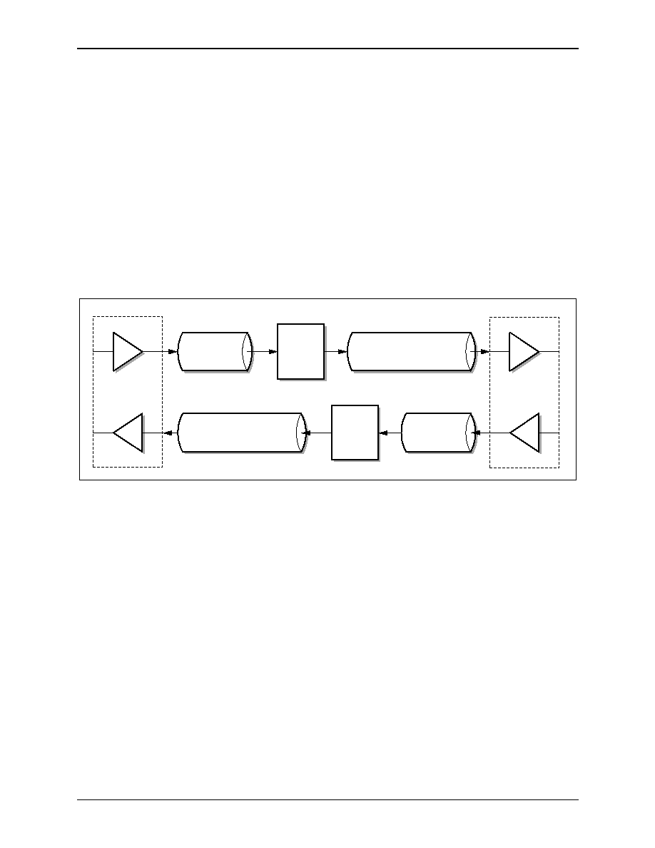
illustrates a typical application using the CX2833i in a
channel.
External pins are provided to configure the various line rates and formats for
each channel.
The CX2833i is used as a data transceiver over a coaxial cable that is up to
900 feet long (or up to 450 feet from the DSX) in an on-premise environment
within any public or private networks which use these data rates.
Figure 2-1. Typical Application Of Single CX2833i Channel
0≠450 ft COAX
(type 734/728)
DSX
0≠450 ft COAX
(type 734/728)
DSX
0≠450 ft COAX
(type 734/728)
0≠450 ft COAX
(type 734/728)
TX
RX
RX
TX
100604_012
CX28331/CX28332/CX28333
2.0 Functional Description
Single/Dual/Triple E3/DS3/STS-1 Line Interface Unit
2.2 Transmitter
100985A
Conexant
2-3
2.2 Transmitter
This section describes the detailed operation of the various blocks in the CX2833i
transmitter.
2.2.1 AMI B3ZS/HDB3 Encoder
ENDECDIS and the E3MODE pins configure the encoder mode.
When ENDECDIS = 0, the encoder is receiving non-encoded Nonreturn to
Zero (NRZ) data on the TNRZ (TPOS) pin alone, and the NC (no connect)
(TNEG) pin is ignored.
Data is encoded into a representation of a three-level B3ZS (E3MODE = 0) or
HDB3 (E3MODE = 1) signal (conforming to the coding rules as specified in
Appendix A
) before going on to the pulse shaper in the form of two binary signals
representing the positive and negative three-level pulses.
When ENDECDIS = 1, the encoder is disabled. The encoder passes
already-encoded data over TPOS (TNRZ) and TNEG (NC) to the pulse shaper.
The transmit digital data is clocked into the chip via a rising TCLK edge,
which must be equal to the symbol rate (line rate). A small delay added to the data
provides a certain amount of negative data hold time.
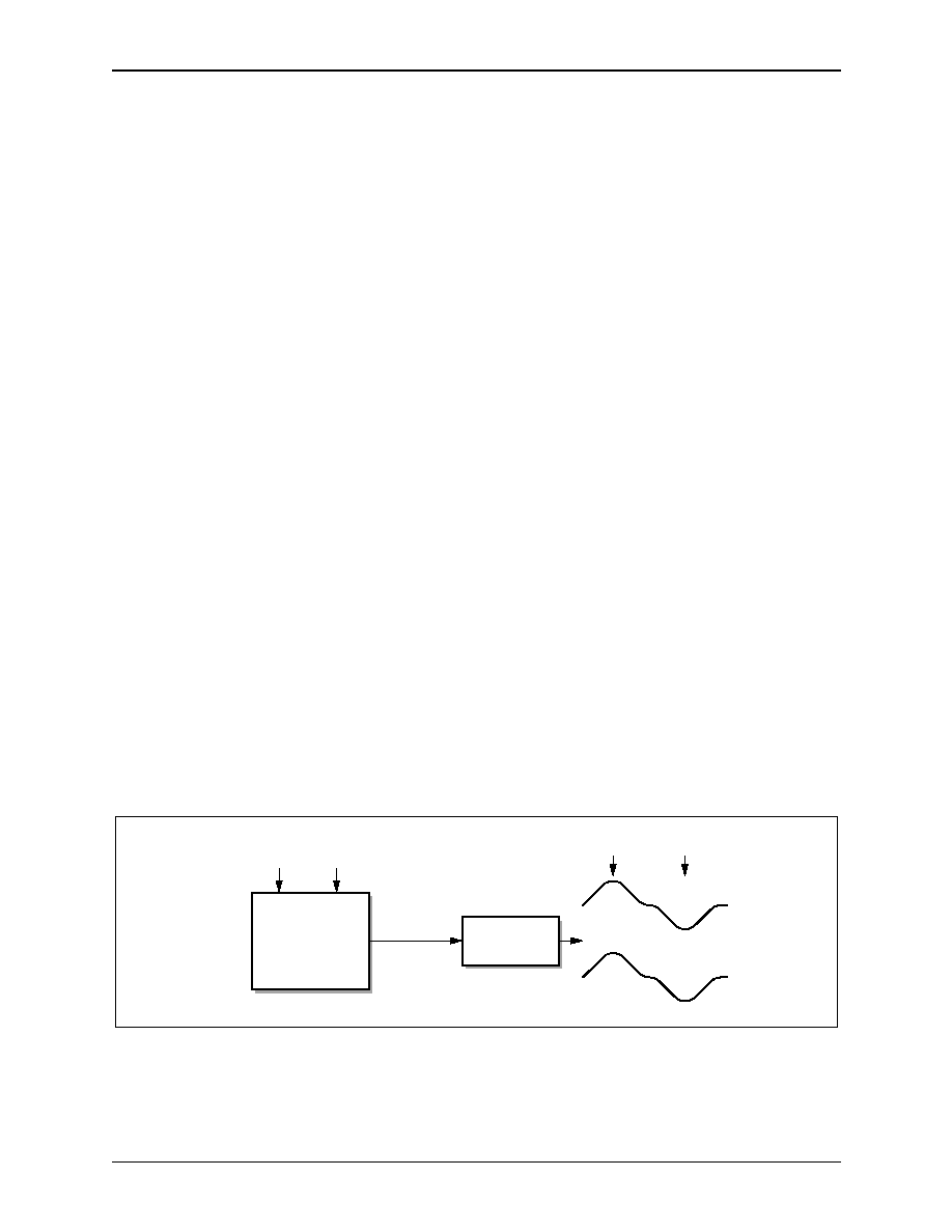
2.2.2 Pulse Shaper
The pulse shaper converts the two digital (clocked) positive and negative pulses
into a single analog three-level Alternate Mark Inversion (AMI) pulse. The pulses
are in Return to Zero (RZ) format, meaning that all positive and negative pulses
have a duration of the first half of the symbol period.
For the E3 rate (E3MODE = 1), the AMI pulse is a full-amplitude,
square-shaped pulse with very little slope.
Figure 2-2. Pulse Shaper
100604_008
Pulse
Shaper
LBO
E3
Mode
LBO = 0
LBO = 1
+ Pulse
≠ Pulse
Line Driver
2.0 Functional Description
CX28331/CX28332/CX28333
2.2 Transmitter
Single/Dual/Triple E3/DS3/STS-1 Line Interface Unit
2-4
Conexant
100985A
For DS3/STS-1 rates, a pulse-shaper block is used to shape the transmit
waveform and reduce its high-frequency energy content. This ensures that the
transmit pulse template is met at the cross-connect block, which follows 0≠450
feet of transmit-side coaxial cable.
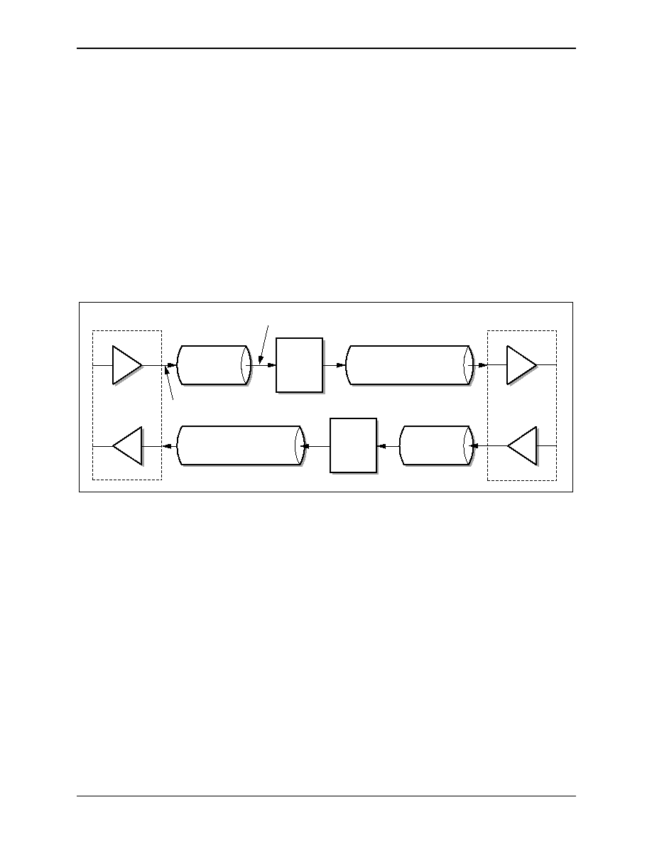
2.2.3 Line Driver
The differential line driver takes the filtered transmit waveform, increases it to the
proper level, and drives it into the transmit magnetics. The two external discrete
back-matching resistors (36
) aid in line matching. The driver is presented with
an approximately 150
differential load. Driver gain accounts for the 6 dB gain
loss in the back-matching resistors.
Figure 2-3
illustrates the Pulse/Power template measurement points for the
various data rates.
Figure 2-3. Pulse Measurement Points
0≠450 ft COAX
(type 734/728)
DSX
0≠450 ft COAX
Pulse/Power Template for E3
Pulse/Power Template for DS3/STS-1
(type 734/728)
DSX
0≠450 ft COAX
(type 734/728)
0≠450 ft COAX
(type 734/728)
TX
RX
RX
TX
100604_013
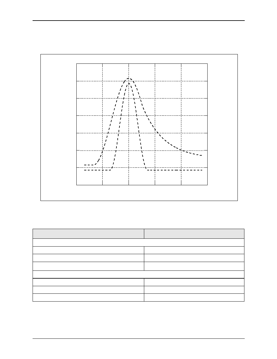
CX28331/CX28332/CX28333
2.0 Functional Description
Single/Dual/Triple E3/DS3/STS-1 Line Interface Unit
2.2 Transmitter
100985A
Conexant
2-5
2.2.3.1 Transmit Pulse
Mask Templates
Figure 2-4. Transmit Pulse Mask for DS3 Rates
Transmit Pulse Mask for STS-1 Rates
1
0.5
0
0.5
1
1.5
Normalized Symbol Time
Nor
m
aliz
ed Pulse Amplitude
1.2
1
0.8
0.6
0.4
0.2
0
0.2
100985_014
Table 2-1. DS3 Transmit Template Specifications
Time Axis Range (UI)
Normalized Amplitude Equation
Upper Curve
≠0.85
T
≠0.68
0.03
≠0.68
T
0.36
0.03 + 0.5 {1 + sin [(pi / 2)(1 + T / 0.34)]}
0.36
T
1.4
0.08 + 0.407 e
≠1.84(T ≠ 0.36)
Lower Curve
≠0.85
T
≠0.36
≠0.03
≠0.36
T
0.36
≠0.03 + 0.5{1 + sin[(pi / 2)(1 + T / 0.18)]}
0.36
T
1.4
0.03
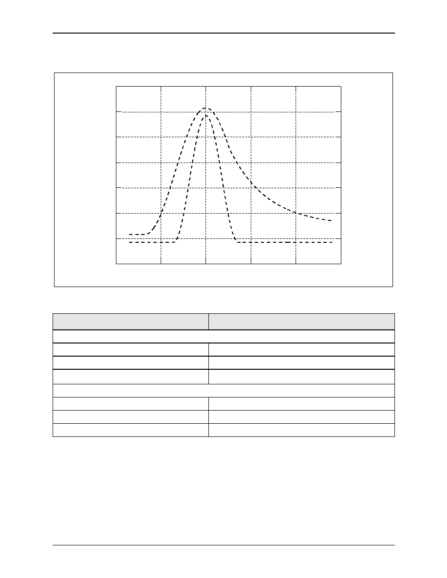
2.0 Functional Description
CX28331/CX28332/CX28333
2.2 Transmitter
Single/Dual/Triple E3/DS3/STS-1 Line Interface Unit
2-6
Conexant
100985A
Figure 2-5. Transmit Pulse Mask for STS-1 Rates
Transmit Pulse Mask for STS-1 Rates
1
0.5
0
0.5
1
1.5
Normalized Symbol Time
Nor
maliz
ed Pulse Amplitude
1.2
1
0.8
0.6
0.4
0.2
0
0.2
100985_014
Table 2-2. STS-1 Transmit Template Specifications
Time Axis Range (T)
Normalized Amplitude Equation
Upper Curve
≠0.85
T
≠0.68
0.03
≠0.68
T
0.26
0.03 + 0.5{1 + sin[(pi / 2)(1 + T / 0.34)]}
0.26
T
1.4
0.1 + 0.61 e
≠2.4(T ≠ 0.26)
Lower Curve
≠0.85
T
≠0.38
≠0.03
≠0.38
T
0.36
≠0.03 + 0.5{1 + sin[(pi / 2)(1 + T / 0.18)]}
0.36
T
1.4
0.03
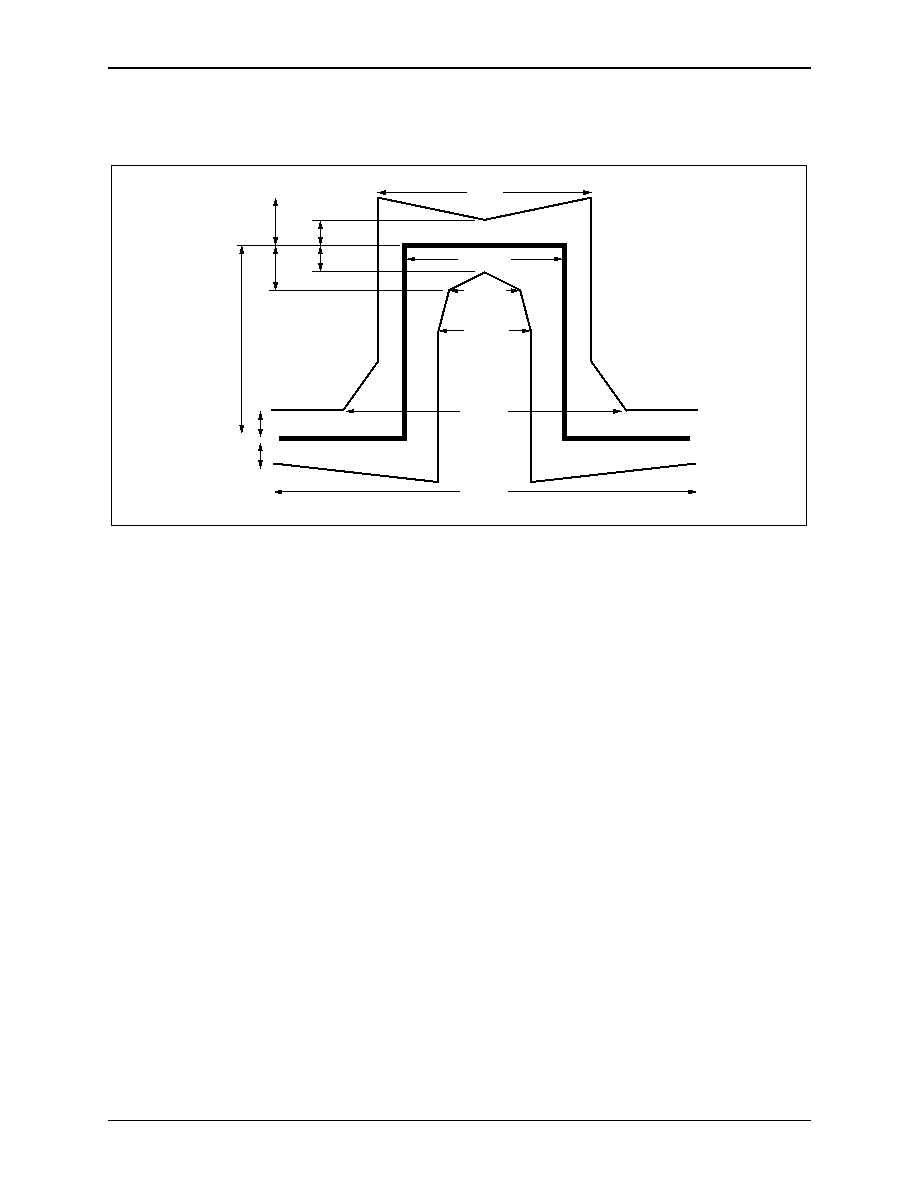
CX28331/CX28332/CX28333
2.0 Functional Description
Single/Dual/Triple E3/DS3/STS-1 Line Interface Unit
2.2 Transmitter
100985A
Conexant
2-7
Figure 2-6. Transmit Pulse Mask for E3 Rate
100985_007
17 ns
0.1
0.1
0.1
0.1
0.1
0.2
0.2
14.55 ns
8.65 ns
12.1 ns
24.5 ns
29.1 ns
Time
Volts
Normalized
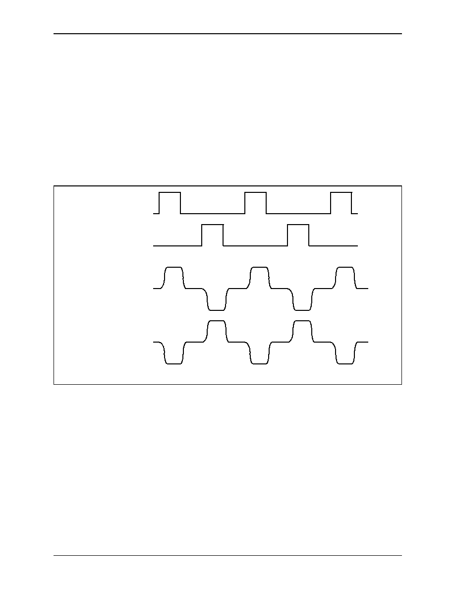
2.0 Functional Description
CX28331/CX28332/CX28333
2.2 Transmitter
Single/Dual/Triple E3/DS3/STS-1 Line Interface Unit
2-8
Conexant
100985A
2.2.4 Alarm Indication Signal (AIS) Generator
When TAIS is asserted, an AIS replaces the transmit data at TPOS and TNEG.
The E3 type of AIS signal (all 1s) is supported. In three-level signal form, this is a
continuously alternating positive and negative pulse stream, as if the transmit data
were a continuous string of logical 1s.
Figure 2-7
illustrates the AIS signal.
The TAIS pin has the same data latency as the TX data pins and can be used to
replace single symbols within a data stream. When the encoder is disabled
(ENDECDIS = 1), the TAIS mode maintains the proper phase, based upon the
polarity of the last 1 received.
The AIS signal follows the same path as the TX data during remote or local
loopback.
2.2.5 Transmit Monitor Block (CX2833i-3x Only)
The transmit monitor inputs (TMONP and TMONM) are designed to monitor the
line driver outputs (TLINEP and TLINEM/N) for pulses and to assert a Loss Of
Signal (TLOS) indicator when no output pulse has been detected for 32 TCLK
periods. After TLOS is asserted, it will not deassert until a pulse is again
detected. The transmit monitor is an independent function in which TMONP and
TMONM must be externally connected to TLINEP and TLINEM/N, respectively.
A special pin (TMONTST) is available for testing board-level functionality
downstream from the TLOS outputs. When TMONST is high it will assert all
TLOS channel outputs. TLOS outputs are active high when the monitor inputs do
not detect a signal.
Figure 2-7. AIS Signal
POSITIVE
PULSE
NEGATIVE
PULSE
TLINEP
(output voltage)
TLINEN
(output voltage)
8333_009

CX28331/CX28332/CX28333
2.0 Functional Description
Single/Dual/Triple E3/DS3/STS-1 Line Interface Unit
2.2 Transmitter
100985A
Conexant
2-9
2.2.6 Jitter Generation (Intrinsic)
The CX2833i device meets the jitter generation requirements for various rates
with large margins, with the condition that the input transmit clock (TCLK) is
jitter-free. Data rates and jitter generation requirements are defined in the
following documents:
∑
E3 rate--ETSI TBR24, ITU-T 9.823
∑
DS3 rate--Bellcore Telecardia GR499, AT&T Accunet TR54014,
ITU-T 9.824
∑
STS-1 rate--Bellcore Telecardia GR253

2.0 Functional Description
CX28331/CX28332/CX28333
2.3 Receiver
Single/Dual/Triple E3/DS3/STS-1 Line Interface Unit
2-10
Conexant
100985A
2.3 Receiver
This section describes the detailed operation of the various blocks in the CX2833i
receiver.
2.3.1 Receive Sensitivity
The receiver recovers data from the coaxial cable that is attenuated due to the
frequency-dependent characteristics of the cable. In addition, the receiver
compensates for the flat loss (across all frequencies) in the various electrical
components and the variation in transmitted signal power.
The CX2833i device is able to recover data that has been attenuated by a
maximum of 900 feet of coax having characteristics and attenuation consistent
with ANSI T1.102-1993, Annex C, Figure C.2. This approximates the
characteristics of AT&T type 734/728 cable; almost the same attenuation
characteristic is achieved by one-half the length of AT&T type 735 cable.
2.3.2 AGC/VGA Block
The Variable Gain Amplifier (VGA) receives the AMI input signal from the
coaxial cable. The VGA supplies flat gain (independent of frequency) to make up
for various flat losses in the transmission channel and for loss at one-half the
symbol rate that cannot be made up by the equalizer. The VGA gain is controlled
by a feedback loop which senses the amplitude of the equalizer output, acting to
servo this amplitude for optimal slicing.
2.3.3 Receive Equalizer
The receive equalizer receives the differential signal from a VGA and acts to
boost the high frequency content of the signal to reduce inter-symbol interference
(ISI) to the point that correct decisions can be made by the slicer with a minimum
of jitter in the recovered data.
The REQH pin is provided to allow lower amounts of equalization (shorter
equivalent cable lengths) for cases where a square-shaped pulse (that does not
meet the DS3/STS-1 standards) is transmitted to the receiver. A square-shaped
input has a much larger high-frequency content and could have overshoots at the
EQ output high enough to cause bit errors. Setting REQH = 0 will lower the gain
and reduce the amount of overshoot.

CX28331/CX28332/CX28333
2.0 Functional Description
Single/Dual/Triple E3/DS3/STS-1 Line Interface Unit
2.3 Receiver
100985A
Conexant
2-11
2.3.4 The PLL Clock Recovery Circuit
The clock recovery circuit (RX PLL) extracts the embedded clock from the sliced
data and provides this clock and the retimed data to the decoder (data mode).
Upon startup (after the internal reset is deasserted), the RX PLL uses a reference
clock (REFCLK, running at the symbol rate) and a phase-frequency detector to
lock to the correct data rate (reference mode). During reference mode, the data
outputs are squelched (set to 0). The RX PLL is kept in reference mode until a
valid input is detected.
2.3.5 Loss Of Signal (LOS) Detector
The Receive Loss Of Signal (RLOS) is a digital function which monitors the
retimed data from the clock recovery block. The AMI data is checked for a
continuous run of zeroes. When a continuous run of 128 ± 1 consecutive zeroes
occurs, the RLOS signal is asserted. After the RLOS signal is asserted, a 1s count
is made on every block of 128 AMI symbols. The RLOS signal is deasserted
when the 1s count within a block of 128 symbols is at least:
B3ZS: Minimum 1s density = 39 ± 1 count out of 128 (~30.5%)
HDB3: Minimum 1s density = 29 ± 1 count out of 128 (~22.7%)
The RLOS detector will always monitor the cable-side RX inputs. The
detector is not affected by the state of remote or local looping.
2.3.6 B3ZS/HDB3 Decoder With Bipolar Violation Detector
In the CX2833i device, when ENDECDIS = 0 (encoder/decoder enabled), the
decoder takes the output from the clock recovery circuit and decodes the data
(HDB3 or B3ZS) into a single retimed NRZ data signal. The data signal is then
sent out of the CX2833i over the RNRZ (RPOS) pin. Any detected Line Code
Violations (LCV) are sent out over the corresponding RLCV (RNEG) pin. The
RLCV pin is asserted for one symbol period at the time the violation appears on
the RX output pin (RNRZ).
The following shows data sequence criteria for LCV; violations are indicated
in bold text. A valid bipolar pulse is indicated by a B. A bipolar violation
(non-alternating positive or negative) pulse is indicated by a V.
∑
Excessive zeros: 0, 0, 0, 0 (HDB3) or 0, 0, 0 (B3ZS). These violations are
passed on as 0 data on the RNRZ pin.
∑
Bipolar violation: B, 0, V (i.e., +1, 0, +1 or -1, 0, -1 for HDB3) B, V
(B3ZS and HDB3). These violations are passed on as 1 data on the RNRZ
pin.
∑
Coding violation: 0, 0, V (HDB3) or 0, V (B3ZS) with an even number of
Bs since the last valid 0 substitution V (follows coding rule). These
violations are passed on as 0 data on the RNRZ pin.
The even/odd counter (used to count the number of Bs between Vs) will count
a bipolar violation as a B. A coding violation or a valid 0 substitution resets the
counter.

2.0 Functional Description
CX28331/CX28332/CX28333
2.3 Receiver
Single/Dual/Triple E3/DS3/STS-1 Line Interface Unit
2-12
Conexant
100985A
When ENDECDIS = 1, the decoder is disabled, and the retimed slicer outputs
are sent out over RPOS (RNRZ) and RNEG (RLCV) pins. These outputs are then
decoded by the Framer or other downstream device. Line code violations are not
detected in this mode of operation. The decoder is configurable for either:
∑
E3 mode using HDB3 coding (E3MODE = 1)
∑
DS3/STS-1 mode using B3ZS coding (E3MODE = 0)
The receiver digital data outputs are centered on the rising edge of RCLK
(see
Section 2.9
).
2.3.7 Data Squelching
A counter in the receiver keeps track of the number of consecutive symbol
periods without a valid data pulse. When 128 or more 0s in a row are counted, the
receiver assumes that it has lost the signal and resets itself to try and regain the
signal. While the receiver is reacquiring the signal, the clock recovery block locks
to the reference clock and the data squelching is achieved by forcing the data bits
to zero. The data squelching is true in both NRZ and dual rail mode. When the
input signal has been properly amplified and equalized, the clock recovery PLL
will then switch to the incoming data.

CX28331/CX28332/CX28333
2.0 Functional Description
Single/Dual/Triple E3/DS3/STS-1 Line Interface Unit
2.4 Jitter Tolerance
100985A
Conexant
2-13
2.4 Jitter Tolerance
The CX2833i receiver is able to tolerate a specified amount of high-frequency
jitter in the received signal while providing error-free operation (generally
defined as a bit error rate of less than 10
-9
). The specifications (illustrated in
Figure 2-9
) for jitter tolerance are discussed in the following documents:
∑
E3 rate ≠ ITU-T G.823 and ETSI TBR24 contain frequency masks for input
jitter tolerance.
NOTE:
To meet jitter transfer requirements for loop-timed operation, an external
jitter attenuator is required. The jitter attenuator lessens jitter from the
receive clock.
∑
DS3 rate ≠ ITU-T G.823 and Bellcore GR499 specify jitter tolerance
frequency masks for Category I and Category II interfaces.
∑
STS-1 rate ≠ Bellcore GR253 specifies a jitter tolerance. It is noted that the
STS-1 jitter tolerance differs from DS3 requirements only for Category II
interfaces.
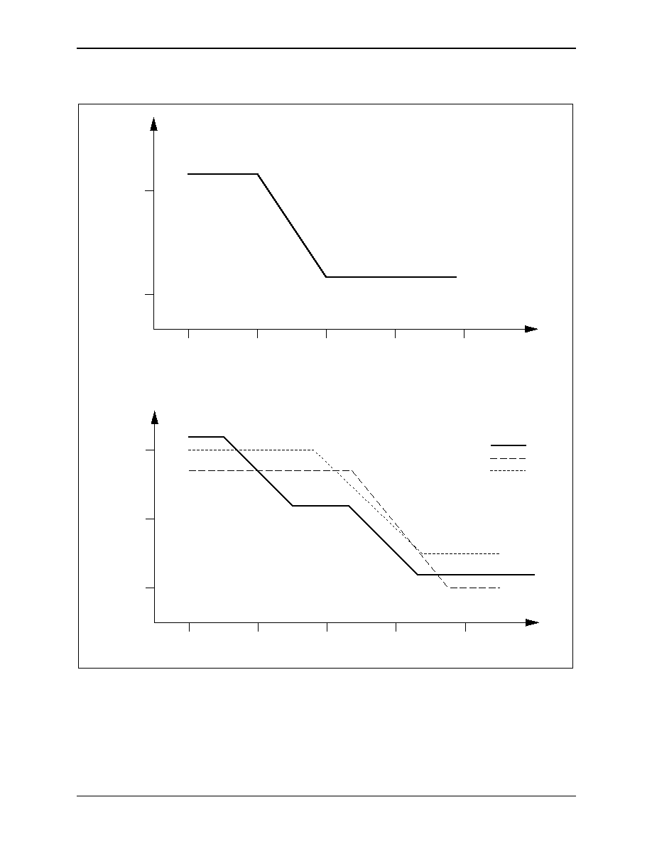
2.0 Functional Description
CX28331/CX28332/CX28333
2.4 Jitter Tolerance
Single/Dual/Triple E3/DS3/STS-1 Line Interface Unit
2-14
Conexant
100985A
Figure 2-8. Minimum Jitter Tolerance Requirement
DS3 / STS-1 Rates
1.0 UI
0.1 UI
1.0 UI
10 UI
0.1 UI
Jitter Frequency
Jitter Frequency
Input Jitter Amplitude
Input Jitter Amplitude
E3 Rate
STS-1
DS3 Category I
DS3 Category II
100 Hz
1 kHz
10 kHz
100 kHz
1 MHz
10 Hz
100 Hz
10 kHz
100 kHz
1 kHz
100604_014
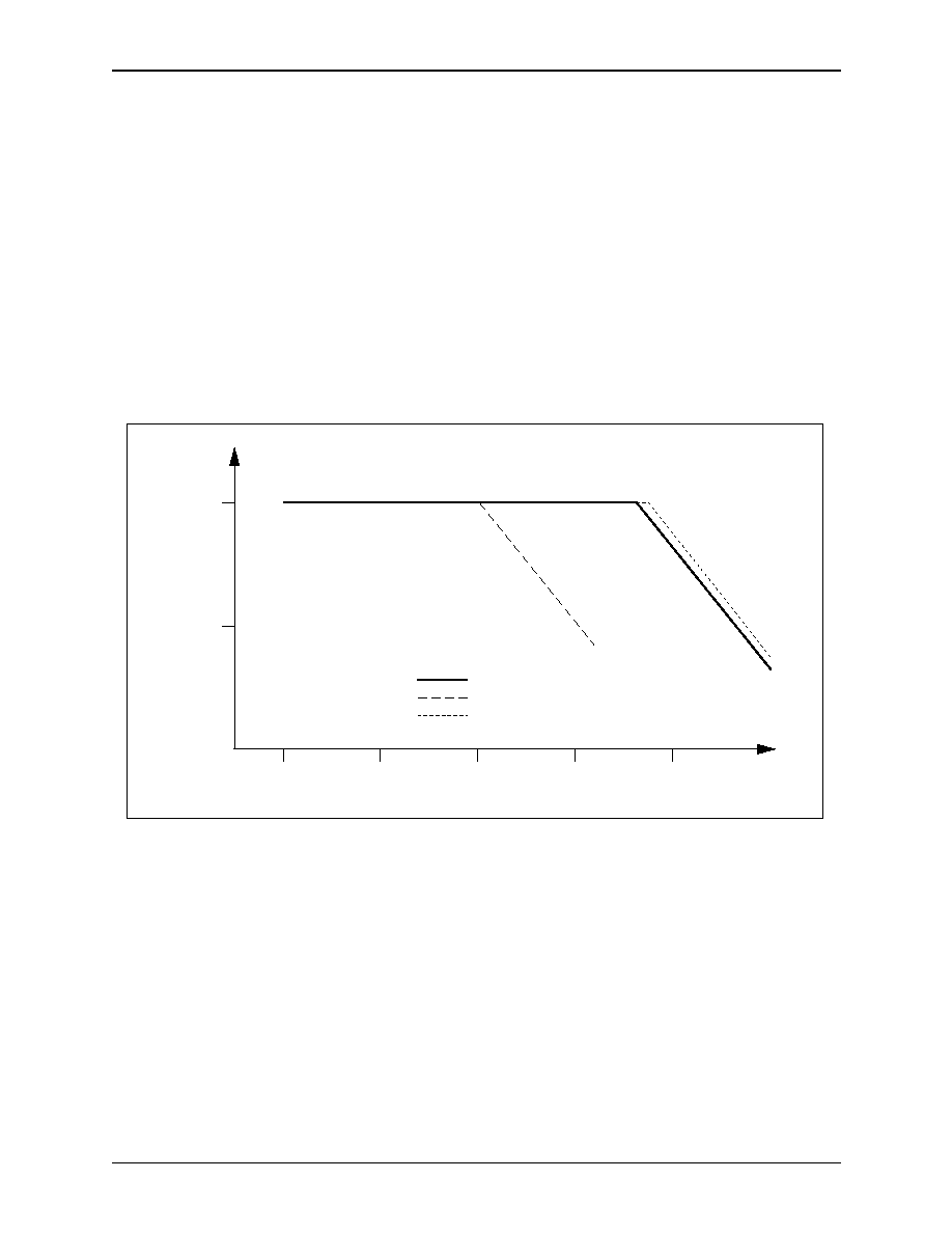
CX28331/CX28332/CX28333
2.0 Functional Description
Single/Dual/Triple E3/DS3/STS-1 Line Interface Unit
2.4 Jitter Tolerance
100985A
Conexant
2-15
2.4.1 Jitter Transfer
The receiver must meet certain jitter transfer specifications between the input and
output jitter as a function of frequency. These specifications are only intended to
be met with the use of a jitter attenuator. Because the CX2833i does not contain a
jitter attenuator, one will have to be supplied externally. For reference purposes,
the specifications are discussed in the following documents and shown in
Figure 2-9
.
E3 rate--Assume the same as DS3.
DS3 rate--Bellcore GR499, section 7.3.2 and figures 7-3, 7-4, and 7-5,
defines and describes DS3 jitter transfer.
STS-1 rate--Bellcore GR253, section 5.6.2.1, defines and describes jitter
transfer for the STS-1 rate.
Figure 2-9. Maximum Jitter Transfer Curve Requirement
0.1 dB
Jitter Frequency
Jitter Gain
≠19.9 dB
STS-1 Category II
DS3 Category I
DS3 Category II
(Note: All slopes are 20 dB/decade)
10 Hz
100 Hz
1 kHz
10 kHz
100 kHz
100985_012

2.0 Functional Description
CX28331/CX28332/CX28333
2.5 Additional CX2833i Functions
Single/Dual/Triple E3/DS3/STS-1 Line Interface Unit
2-16
Conexant
100985A
2.5 Additional CX2833i Functions
2.5.1 Bias Generator
To achieve good isolation between the channels, each channel utilizes an
independent power and ground to both transmit and receive. Additionally, each
channel has its own band gap voltage reference. Because only one external
resistor for current generation exists, only one band gap voltage can be used. The
band gap from Ch1 has been chosen for this task.
The 12.1 k
external resistor from pin RBIAS to ground, is specified to have
a tolerance of ±1%. This helps to keep tighter control on power dissipation and
circuit performance.
NOTE:
Capacitance should be kept to a minimum on the RBIAS pin.
2.5.2 Power-On Reset (POR)
A POR function is provided in the CX2833i device to ensure all of the resettable
digital logic and analog control lines are starting from a known state. This circuit
uses a fixed RC timer (~1
µ
s); additionally, 128 clocks from REFCLK are counted
(after the RC timer has timed-out) before reset is deasserted, which begins timing
after a minimum supply voltage is reached (see
Table 2-4
).
2.5.3 Loopback Multiplexers (MUXes)
Two loopback MUXes per channel in the CX2833i allow for local loopback
(terminal or framer side), remote loopback (cable side), or both (the AIS signal
follows the same path as the transmit data during loopback). The RLOS signal
monitors the RX cable inputs irrespective of any loopback.
In remote loopback, set by asserting pin RLOOP high, the receive data
(retimed after clock recovery but not decoded) loops back into the pulse shaper in
place of the transmit data. Additionally, this data sent out the RPOS, RNEG, and
RCLK pins.
In local loopback, set by asserting pin LLOOP, the transmit data loops back
immediately from the encoder output to the decoder input in place of the received
data. Additionally, this data is sent out the TLINEP and TLINEM/N pins.
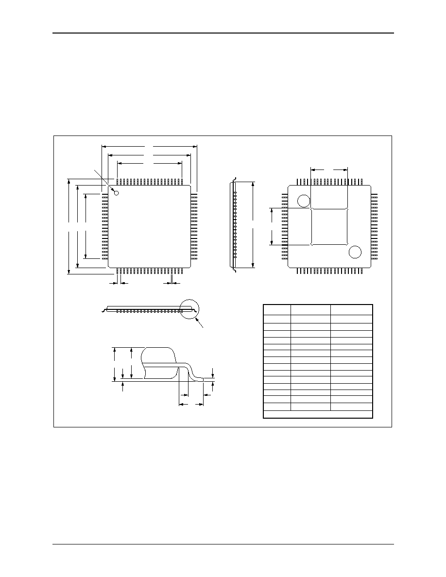
CX28331/CX28332/CX28333
2.0 Functional Description
Single/Dual/Triple E3/DS3/STS-1 Line Interface Unit
2.6 Mechanical Specifications
100985A
Conexant
2-17
2.6 Mechanical Specifications
Figure 2-10. CX2833i-1x Mechanical Drawing (80-Pin)--Dimensions
D
3
D
3
D
D
1
D
1
D
2
D
D
1
D
2
A
L
A
1
L
1
A
2
Pin #1
Ref. Mark
e
b
See DETAIL B
TOP
DETAIL B
BOTTOM
c
Dim.
A
A1
A2
D
D1
D2
D3
L
L1
b
c
e
Coplanarity
0.05
0.95
15.75
13.90
0.45
0.09
1.20 MAX.
12.35 REF.
6.50 REF.
1.00 REF.
0.32 REF.
0.65 REF.
0.10 MAX.
0.15
1.05
16.25
14.10
0.75
0.20
0.002
0.040
0.620
0.547
0.018
0.004
0.047 MAX.
0.486 REF.
0.256 REF.
0.039 REF.
0.013 REF.
0.026 REF.
0.004 MAX.
0.006
0.041
0.640
0.555
0.030
0.008
Ref. 80-Pin ETQFP (GP00-D537)
Millimeters
Inches
Min.
Max.
Min.
Max.
100985_008
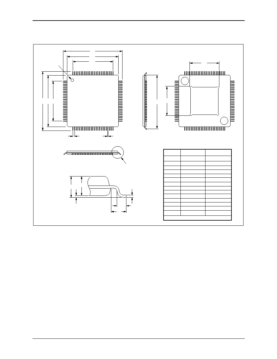
2.0 Functional Description
CX28331/CX28332/CX28333
2.6 Mechanical Specifications
Single/Dual/Triple E3/DS3/STS-1 Line Interface Unit
2-18
Conexant
100985A
Figure 2-11. CX2833i-3x Mechanical Drawing (100-Pin)--Dimensions
D
3
D
3
D
D
1
D
1
D
2
D
D
1 D2
A
L
A
1
L
1
A
2
Pin #1
Ref. Mark
e
b
See DETAIL B
TOP
DETAIL B
BOTTOM
c
Dim.
A
A1
A2
D
D1
D2
D3
L
L1
b
e
c
Coplanarity
0.05
0.95
15.75
13.90
0.45
0.09
1.20 MAX.
12.00 REF.
8.00 REF.
1.00 REF.
0.22 REF.
0.50 REF.
0.08 MAX.
0.15
1.05
16.25
14.10
0.75
0.20
0.002
0.004
0.620
0.547
0.018
0.004
0.047 MAX.
0.472 REF.
0.315 REF.
0.039 REF.
0.009 REF.
0.020 REF.
0.004 MAX.
0.006
0.041
0.640
0.555
0.006
0.008
Ref. 100-Pin ETQFP (GP00-D543)mm
Millimeters
Inches
Min.
Max.
Min.
Max.
100985_008a

CX28331/CX28332/CX28333
2.0 Functional Description
Single/Dual/Triple E3/DS3/STS-1 Line Interface Unit
2.7 Electrical Characteristics
100985A
Conexant
2-19
2.7 Electrical Characteristics
2.7.1 Absolute Maximum Ratings
Table 2-3. Absolute Maximum Ratings
Symbol
Parameter
Min
Max
Unit
DVDDC/
RVDD/
TVDD/
VDD
Power Supply Voltage
≠0.3
6
V
V
I
Voltage on Any Signal Pin
≠1.0
VGG + 0.3 V
V
T
ST
Storage Temperature
≠40
125
∞C
T
VSOL
Vapor Phase Soldering
Temperature (1 min.)
--
220
∞C
JA
Thermal Resistance (Still
air, socketed)
--
40
∞
C
/
W
JA
Thermal Resistance (Still
air, soldered)
--
24
∞
C
/
W
Jc
--
--
7.40
∞
C
/
W
FIT
Failures in time @ 89,000
device hours, temperature
of 55 ∞C, 0 failures.
--
313
fits
NOTE(S):
1. Stresses above those listed as absolute maximum ratings may cause permanent damage
to the device. This is a stress rating only, and functional operation of the device at these or
any other conditions beyond those indicated in the other sections of this document is not
implied. Exposure to absolute maximum rating conditions for extended periods may affect
device reliability.

2.0 Functional Description
CX28331/CX28332/CX28333
2.7 Electrical Characteristics
Single/Dual/Triple E3/DS3/STS-1 Line Interface Unit
2-20
Conexant
100985A
2.7.2 Recommended Operating Conditions
Table 2-4
specifies various operating conditions, power supplies, and the bias
resistor.
Table 2-4. Recommended Operating Conditions
Parameter
Conditions
Min
Nom
Max
Unit
Power supply voltage
DVDDC, RVDD, TVDD,
VDD
3.135
3.3
3.465
V
ESD voltage
(1)
VGG
3.135
5
5.5
V
Power dissipation
(CX28333)
Total chip
--
0.83
1.0
W
Power dissipation
(CX28332)
Total chip
--
--
0.8
W
Power dissipation
(CX28331)
Total chip
--
--
.450
W
External bias resistor
Pin RBIAS to GND; ±1%
11.98
12.1
12.22
k
NOTE(S):
(1)
With 5 V logic input, VGG should be tied to 5 V. With 3.3 V logic input, VGG should be tied
to 3.3 V.

CX28331/CX28332/CX28333
2.0 Functional Description
Single/Dual/Triple E3/DS3/STS-1 Line Interface Unit
2.8 DC Characteristics
100985A
Conexant
2-21
2.8 DC Characteristics
Table 2-5. DC Characteristics
Parameter
Conditions
Min
Nom
Max
Unit
V
ih
high threshold
Digital inputs
2.0
--
VGG + 0.3
V
V
il
low threshold
Digital inputs
≠0.3
--
0.8
V
V
oh
high threshold
Digital outputs, I
oh
= ≠4 mA
2.4
--
--
V
V
ol
low threshold
Digital outputs, I
ol
= 4 mA
--
--
0.4
V
I
LEAK
0 V
digital Vin
VGG
≠10
--
200
µ
A
Input capacitance
--
--
--
10
pF
Load capacitance
Digital outputs
--
--
15
pF
NOTE(S):
1. The digital inputs of CX2833i are TTL 5 V compliant. These inputs are diode protected to DVDDIO and DVSSIO pins.
Additionally, all of the CX2833i digital inputs contain 75 k
pull-down resistors.
2. The digital outputs of CX2833i are also TTL 5 V compliant. However, these outputs will not drive to 5 V, nor will they accept
5 V external pull-ups. The output is DVDDC (3.3 V).
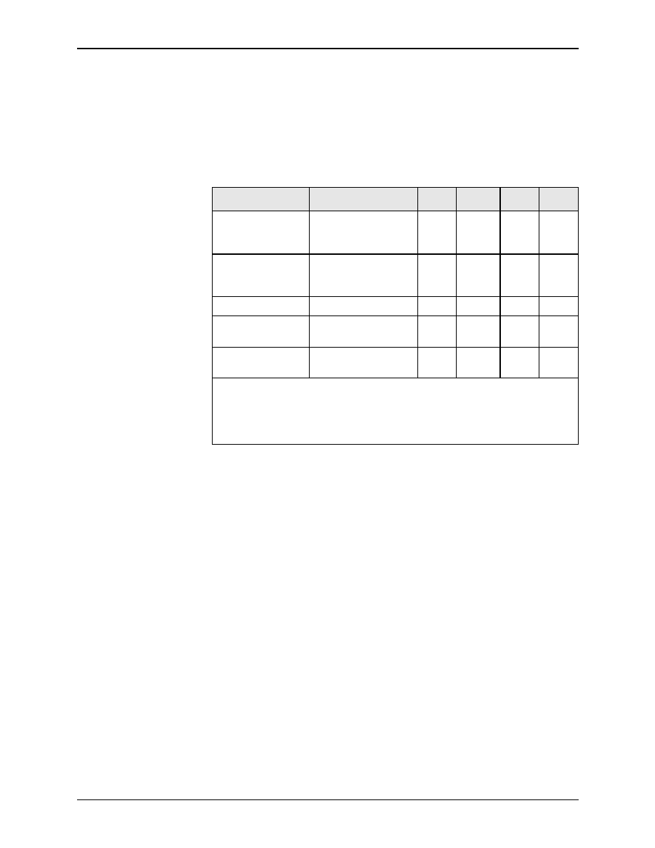
2.0 Functional Description
CX28331/CX28332/CX28333
2.9 AC Characteristics
Single/Dual/Triple E3/DS3/STS-1 Line Interface Unit
2-22
Conexant
100985A
2.9 AC Characteristics
Table 2-6. AC Characteristics (Logic Timing)
Parameter
Conditions
Min
Nom
Max
Unit
Tosym, Tisym
RCLK and TCLK
E3
DS-3
STS-1
--
29.10
22.35
19.29
--
ns
ns
ns
Clock Duty Cycle
Towidth/Tosym, RCLK
Tiwidth/Tisym, TCLK
Tiwidth/Tisym, REFCLK
45
40
40
--
55
60
60
%
%
%
Todelay
--
--
--
3
ns
Tisetup
TPOS/TNRZ, TNEG,
TAIS
4
--
--
ns
Tihold
TPOS/TNRZ, TNEG,
TAIS
0
--
--
ns
NOTE(S):
1. The description applies to the DS3, E3, and STS-1 clock rates and other parameters such
as pulse width, set-up time, hold time, and duty cycle.
2. The timing diagram, illustrated in
Figure 2-12
, describes the logical relationship between
various clock and data signals, and parameter values.
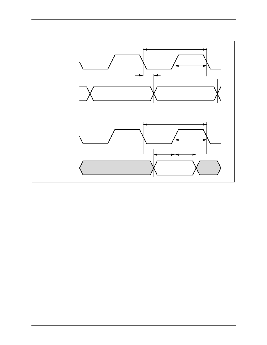
CX28331/CX28332/CX28333
2.0 Functional Description
Single/Dual/Triple E3/DS3/STS-1 Line Interface Unit
2.9 AC Characteristics
100985A
Conexant
2-23
Figure 2-12. Timing Diagram
TCLK
TPOS/TNRZ,
TNEG, TAIS,
Tisym
Tisetup
Tihold
DATA INPUTS
Don't
Care
Valid Data
Tiwidth
RCLK
RPOS/RNRZ,
RNEG/RLCV
Tosym
Todelay
DATA OUTPUTS
Towidth
Don't
Care
100604_016

2.0 Functional Description
CX28331/CX28332/CX28333
2.9 AC Characteristics
Single/Dual/Triple E3/DS3/STS-1 Line Interface Unit
2-24
Conexant
100985A

100985A
Conexant
3-1
3
3.0 Applications
The CX28331/CX28332/CX28333 can be used in a variety of applications.
Figure 3-1
illustrates an example of three DS3 lines being terminated by the
CX28333. The data and clock are extracted and passed on to the framer chip for
further data manipulation and user interface.
It is important to employ high-frequency design techniques for the printed
board layout.
3.1 PCB Design Considerations for CX2833i
The CX28333 device is a triple LIU operating at frequencies up to 52.84 MHz.
The high-speed nature of the device calls for a careful design of the PCB using
this device. Some design considerations are outlined below.
3.1.1 Power Supply and Ground Plane
A unified power plane with properly placed capacitors of the correct size will
mitigate most power rail-related voltage transients. A properly placed bulk
capacitor, where the power enters the board, with noise-bypassing capacitors at
the power pins on the integrated circuits should be adequate. The noise-bypassing
capacitors must be able to supply all the switching current.
Ferrite beads are used with power rails to filter the high-frequency noise. For
every design, noise frequencies and levels are different. Therefore, whether beads
are necessary, and the effective frequency where they should operate, is difficult
to determine. It is a good idea to provision for ferrite beads on the boards.
The board trace from the CX28333 power supply pin to the noise-bypassing
capacitor should be minimized. Additionally, ground connections from the
ground plane to the CX28333 ground pins and the noise-bypassing capacitor
ground pins should be minimized.
A unified ground plane is the best way to minimize ground impedance. Most
of the ground noise is produced by the return currents and power supply transients
during switching. This effect is minimized by reducing the ground plane
impedance.

3.0 Applications
CX28331/CX28332/CX28333
3.1 PCB Design Considerations for CX2833i
Single/Dual/Triple E3/DS3/STS-1 Line Interface Unit
3-2
Conexant
100985A
3.1.2 Impedance Matching
It is critical that traces around the transformers and matching resistors be kept to a
minimum length and, in the following cases, the trace impedance be matched to
75
with a
±
10% tolerance:
∑
The impedance from the BNC connector to the transformer
∑
The impedance from the transformer to the matching resistors
3.1.3 Other Passive Parts
The reference design uses the Pulse T3001 extended temperature range 1:1
transformer for the coupling of the BNC connector to the device.
The ferrite beads used to decouple the receive- and transmit-VDD pins on all
analog input VDD pins are type 2508056017Y0 from Fair-Rite Products
Corporation. The bulk capacitor used for where the power enters the board
should be a tantulum≠type capacitor, the recommended value and type is a 220
µ
f
tantulum capacitor.
3.1.4 IBIS Models
IBIS (Input/Output Buffer Interface Specification) models for the
CX28331/CX28332/CX28333-1x and -3x are available from Conexant's web site
(www.conexant.com).
3.1.5 Recommended Vendors
Product: Transformers
Product: Ferrite Beads
America
Address:
Telo:
Fax:
Pulse
Corporate Office
12220 World Trade Drive
San Diego, CA 92128
858-674-8100
858-674-8262
Telo:
Web site:
Fair-Rite Products Corp.
P.O. Box J
One Commercial Row
Wallkill, NY 12589
914-895-2055
www.Fair-Rite.com
Northern Asia
Telo:
Pulse
3F-4, No. 81, Sec. 1
Hsin Tai Wu Road
Hsi-Chih
Tapei Hsien, Taiwan
R.O.C.
886-2-26980228
886-2-26980948
Product: Crystals
Northern Europe
Telo:
Fax:
Pulse
1S2 Huxley Road
The Surrey Research Park
Guildford, Surrey GU2 5RE
United Kingdom
44-1483-401700
44-1483-401701
Telo:
Fax:
E-mail:
Web site:
Crystek Corp.
12730 Commonwealth Drive
Fort Myers, FL 33913
800-237-3061
941-561-1025
sales@crystek.com
www.crystek.com
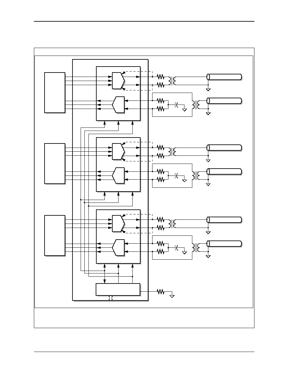
CX28331/CX28332/CX28333
3.0 Applications
Single/Dual/Triple E3/DS3/STS-1 Line Interface Unit
3.1 PCB Design Considerations for CX2833i
100985A
Conexant
3-3
Figure 3-1.
NOTE(S):
1. All transformers are part number T3001 from Pulse Technology. See Recommended Vendors,
Section 3.1.5
.
2. TMONP and TMONM are only available on the CX2833i-3x device and are denoted by dotted lines.
TX
TPOS
TNEG
TCLK
TLINEP
TLINEN
RX
RLINEP
RNEG
RLINEN
RPOS
RCLK
MODE
BIAS
RESET
Channel 1
CX28333
Framer
37.4
9
37.4
9
31.6
9
31.6
9
0.01µF
1:1
1:1
Type 728, 734, 735
75
9
Type 728, 734, 735
75
9
TX
TPOS
TNEG
TCLK
TLINEN
RX
RLINEP
RNEG
RLINEN
RPOS
RCLK
MODE
BIAS
RESET
Channel 2
TLINEP
TLINEP
TMONP
TMONM
TMONP
TMONM
TMONP
TMONM
Framer
37.4
9
37.4
9
31.6
9
31.6
9
0.01µF
1:1
1:1
Type 728, 734, 735
75
9
Type 728, 734, 735
75
9
TX
TPOS
TNEG
TCLK
TLINEN
RX
RLINEP
RNEG
RLINEN
RPOS
RCLK
MODE
BIAS
RESET
Channel 2
Framer
37.4
9
37.4
9
31.6
9
31.6
9
0.01µF
1:1
1:1
Type 728, 734, 735
75
9
Type 728, 734, 735
75
9
MODE
BIAS
RESET
RBIAS
12.1K
9
Mode/Status Pins
100985_009

3.0 Applications
CX28331/CX28332/CX28333
3.1 PCB Design Considerations for CX2833i
Single/Dual/Triple E3/DS3/STS-1 Line Interface Unit
3-4
Conexant
100985A

100985A
Conexant
A-1
A
Appendix A
A.1 Applicable Standards
The applicable standards documents are as follows:
∑
ANSI T1.102-1993 (DS3 and STS-1 standard)
∑
ANSI T1.404a-1996 (DS3 metallic interface)
∑
ITU Recommendation G.703 (DS3 and E3 standard)
∑
ITU Recommendation G.823 and G.824 (jitter and wander)
∑
Bellcore GR499, Issue 1, 12/89 (formerly TR-TSY-000499)
(DS3 and STS-1 requirements)
∑
Bellcore GR253, Issue 2, 12/91 (formerly TA-NWT-000253)
(STS-1 requirements and jitter)
∑
Bellcore TR-TSY-000191, Issue 1, 5/86 (AIS and LOS)
∑
ETSI TBR24 and TBR25 (E3 terminal equipment interface)
∑
ETSI ETS 300 686 and ETS 300 687 (E3 standard)
∑
AT&T Technical Reference TR54014, May 1992 (Accunet Interface
Specification for DS-3 jitter only)

Appendix A
CX28331/CX28332/CX28333
A.1 Applicable Standards
Single/Dual/Triple E3/DS3/STS-1 Line Interface Unit
A-2
Conexant
100985A

100985A
Conexant
B-1
B
Appendix B
B.1 Evaluation Module Schematic
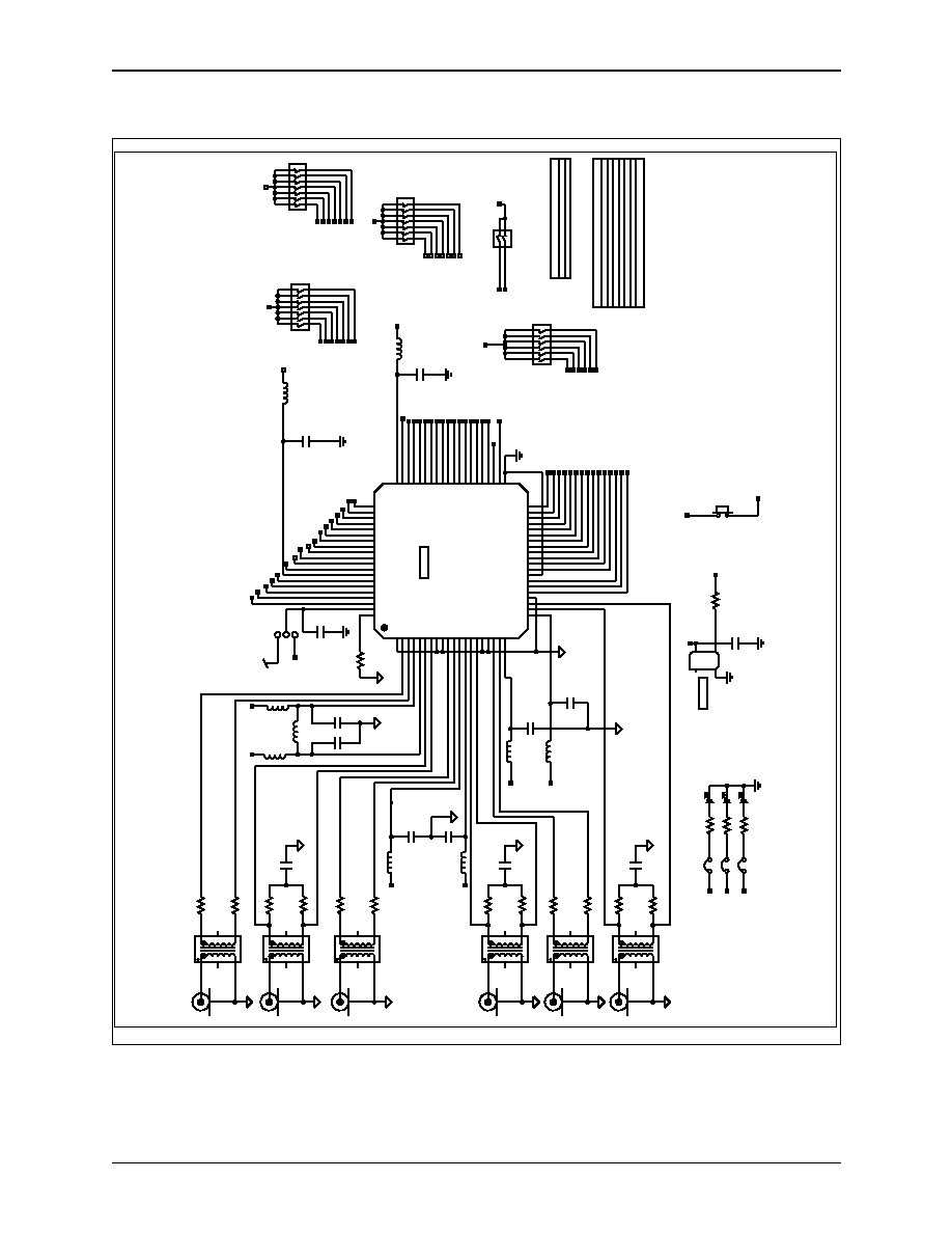
Appendix B
CX28331/CX28332/CX28333
B.1 Evaluation Module Schematic
Single/Dual/Triple E3/DS3/STS-1 Line Interface Unit
B-2
Conexant
100985A
Figure B-1. Recommended Schematic for the CX2833i-1x Device
P
osition 7 REQH(1=Enab
le Equalization 0=Disab
le)
Pin 2 E3MODE 1=E3 mode is enab
led 0=Disab
led
Pin 1 ENDECDIS 1=Dual r
ail pulse coded data f
o
r
m
at
SOCKET
SOCKET
CHANNEL 3 RECEIVE
CHANNEL 3
TRANSMIT
CHANNEL 2 RECEIVE
DECODER AND E3 SELECTION
CHANNEL 1 RECEIVE
CHANNEL 1
TRANSMIT
CHANNEL 2
TRANSMIT
P
osition 1 PDB PO
WERDO
WN (0=P
o
w
erdo
wn 1=Activ
e)
P
osition 2 RLOOP (1=Remote LPBK Enab
led 0=Disab
led)
P
osition 3 LLOOP (1=Local Loop Enab
led 0=Disab
led)
P
osition 4 LBO (1=TX CABLE less than 250ft 0=g
reater than 250ft)
P
osition 5 XOE (1=T
r
ansmitter Enab
led 0=Disab
led)
P
osition 6
T
A
IS (1=Enab
le AIS oper
ation 0=disab
le)
DIGIT
AL GND
BNC
BNC
BNC
BNC
BNC
CC
CC
CC
CC
CC
CC
CC
BNC
CC
ANALOG GND
CC
CC
CC
CC
CC
CC
CC
2 Pin DIP Switch Setting
Se
v
en P
osition DIP Switch Settings f
or all Channels
CC
CC
CC
CC
CC
CC
CC
CC
CC
CC
CC
CC
CC
CC
CC
CH1_LOS
CH2_LOS
CH3_LOS
7
8
9
6
5
4
3
2
12
11
10
1
SW5
N1
T3001
PULSE
1
2
34
5
6
L2
T3001
PULSE
1
2
34
5
6
L3
1
2
34
5
6
T3001
PULSE
6
5
4
3
2
1
L4
1
2
34
5
6
T3001
PULSE
6
5
4
3
2
1
L5
1
2
34
5
6
T3001
PULSE
1
2
34
5
6
L6
J2
J3
J4
J5
J6
R3
37.4
37.4
R4
R7
37.4
37.4
R8
0.01
C2
R11
37.4
0.01
C3
R12
37.4
J1
T3001
PULSE
6
5
4
3
2
1
L1
1
23
4
4
3
2
1
SW4
J8
J9
J10
14
8
7
1
Y1
2
1
CR3
C1
0.01
31.6
R1
R2
31.6
31.6
R5
31.6
R9
31.6
R10
L15
L7
L11
L10
C4
0.1
0.1
C5
R6
31.6
L13
L12
C6
0.1
0.1
C7
L14
C8
0.1
12.1K
R13
CR1
12
CR2
SW9
C9
0.1
5
10
3
4
6
8
9
11
1
2
7
13
12
14
SW1
5
10
3
4
6
8
9
11
1
2
7
13
12
14
SW2
5
10
3
4
6
8
9
11
1
2
7
13
12
14
SW3
R14
402
402
R15
402
R16
1/4
42.2
R17
C10
0.1
L16
L17
C11
0.1
60
73
41
28
43
59
31
72
44
29
74
56
27
76
58
25
80
67
53
34
65
47
36
70
46
7
6
15
14
23
22
75
57
26
66
52
35
69
55
32
68
54
33
5
13
21
8
16
24
61
51
40
62
3
2
11
10
19
18
78
77
42
64
63
49
38
4
12
20
1
9
17
79
71
45
30
80 ETQFP
CX28333
50
48
39
37
U1
0.1
C12
C13
0.1
2
3
1
J7
T
A
IS3/TMUXA4
XOE3
LBO3
LLOOP3
PDB3
RLOOP3
+3_3V
T
AIS1/TMUXA2
XOE1
LBO1
LLOOP1
PDB1
RLOOP1
+3_3V
RLOS1
RLOS2
RLOS3
GND
NC
OUT
VCC
+3_3V
+3_3V
+3_3V
+3_3V
+3_3V
+3_3V
+3_3V
+5V
TMUXIO1
TMUXIO2
PDB1
RLOOP1
LLOOP1
LBO1
XOE1
REQH1/TMUXD
A
T
RNEG1/RLCV1
RPOS1/RNRZ1
RCLK1
RLOS1
REFCLK
TNEG1/NC1
TPOS1/TNRZ1
TCLK1
T
A
IS1/TMUXA2
PDB2
RLOOP2
LLOOP2
RNEG2/RLCV2
RPOS2/RNRZ2
RCLK2
RLOS2
T
A
IS2/TMUXA3
TPOS2/TNRZ2
REFCLK
REQH2/TMUXA0
XOE2
LBO2
TMUXLA
T
PDB3
RLOOP3
LLOOP3
LBO3
XOE3
REQH3/TMUXA1
RNEG3/RLCV3
RPOS3/RNRZ3
RCLK3
RLOS3
REFCLK
TPOS3/TNRZ3
T
A
IS3/TMUXA4
+3_3V
+3_3V
+3_3V
+3_3V
+3_3V
RLOOP2
PDB2
LLOOP2
LBO2
XOE2
T
A
IS2/TMUXA3
E3MODE
ENDECDIS
ENDECDIS
E3MODE
REQH1/TMUXD
A
T
REQH2/TMUXA0
REQH3/TMUXA1
TMUXLA
T
REFCLK
+3_3V
D
VDD
DVDD2
D
VSS
DVSS2
E3MODE
ENDECDIS
REQH3/TMUXA1
LBO1
LBO2
LBO3
LLOOP1
LLOOP2
LLOOP3
PDB1
PDB2
PDB3
RBIAS
RCLK1
RCLK2
RCLK3
REFCLK1
REFCLK2
REFCLK3
REQH1/TMUXDA
T
REQH2/TMUXA0
RLINE1M
RLINE1P
RLINE2M
RLINE2P
RLINE3M
RLINE3P
RLOOP1
RLOOP2
RLOOP3
RLOS1
RLOS2
RLOS3
RNEG1/RLCV1
RNEG2/RLCV2
RNEG3/RLCV3
RPOS1/RNRZ1
RPOS2/RNRZ2
RPOS3/RNRZ3
R
VDD1
R
VDD2
RVDD3
R
VSS1
R
VSS2
RVSS3
T A
IS1/TMUXA2
T
A
IS2/TMUXA3
T AIS3/TMUXA4
TCLK1
TLINE1M
TLINE1P
TLINE2M
TLINE2P
TLINE3M
TLINE3P
TMUXIO1
TMUXIO2
TMUXLA
T
TNEG1/NC1
TPOS1/TNRZ1
TPOS2/TNRZ2
TPOS3/TNRZ3
TVDD1
TVDD2
TVDD3
TVSS1
TVSS2
TVSS3
VGG
XOE1
XOE2
XOE3
TCLK2
TNEG2/NC2
TCLK3
TNEG3/NC3
TCLK2
TNEG2/NC2
TCLK3
TNEG3/NC3
+3_3V
REQH2/TMUXA0
REQH3/TMUXA1
T
AIS1/TMUXA2
T
AIS2/TMUXA3
T
AIS3/TMUXA4
REQH1/TMUXD
A
T
100985_017
CX28331/CX28332/CX28333
Appendix B
Single/Dual/Triple E3/DS3/STS-1 Line Interface Unit
B.1 Evaluation Module Schematic
100985A
Conexant
B-3
Figure B-2. Recommended Schematic for the CX2833i-3x Device (1 of 2)
NC
Gnd
Out
Vcc
Socket
CH1_RLOS
CH2_RLOS
CH3_RLOS
Position
7
REQH#
(
0
=EQ
Disable
1
=
EQ
Enable)
Position
5
XOE#
(
0
=
Tx
Disable
1
=
Tx
Enable)
Position
2
R
LOOP#
(
0
=
RLPBK
Disable
1
=
RLPBK
Enable)
Position
3
LLOOP#
(
0
=
LPBK
Disable
1
=
LPBK
Enable)
Position
4
LBO#
(
0
=
T
x
Cable
>
250ft
1
=
Tx
Cable
<
250ft)
Position
6
T
AIS#
(
0
=Tx
AIS
Disable
1
=
T
x
AIS
Enable)
Position
1
PDB#
(
0
=
Powerdown
1
=
Active)
Notes:
Seve
n
Position
Dip
switch
for
all
Channels
(SW1,2,3)
CX28333
DS3/E3/STS-1
LIU
CH1_TLOS
CH2_TLOS
CH3_TLOS
Pulse
Pulse
Pulse
Pulse
Pulse
Pulse
2,3,4
2,3,4
2,3,4
2,3,4
2,3,4
2,3,4
N
o
te:
All
capacitors
are
in
Microfarads
Reset
Device
BT01-D
630-
A
CX
28333
(LIU)
w/Jitter
A
ttenuator
Circuit
Conexant
Systems
9868
Scranton
Road
San
Diego,Ca
92121
C
12
Title
S
i
z
e
Document
Number
Rev
D
a
t
e
:
Sheet
of
PD3
RLOOP
3
E3MOD
E
ENDECDIS
REFCLK
REFCLK
RPOS1/RNRZ1
REQH1/TMUX
D
A
T
TCL
K
3
RLOS3
LLOO
P
1
XOE1
TMUXI
O
2
RCLK1
LBO
3
REQH3/TMUX
A
1
LLOO
P
3
TAIS3/
TMUXA4
LBO
3
XOE3
PD2
RLOOP
2
LLOO
P
2
LBO
2
XOE2
T
A
I
S
2
/
TMUXA3
REQH2/TMUX
A
0
RNEG1/RLCV1
RLOOP1
RCLK3
REQH3/TMUX
A
1
REQH2/TMUXA
0
RPOS2/RNRZ2
TAIS2/
TMUXA3
LBO
2
E3MOD
E
T
L
OS2
T
M
UXLAT
RNEG2/RLCV2
RLOOP
2
XOE2
TNEG1/NC1
REFCLK
TPOS2/TNRZ
2
TNEG2/NC2
XOE3
RCLK2
TNEG3/NC3
RLOOP
3
T
L
OS1
RPOS3/RNRZ3
TPOS3/TNR
Z
3
PD1
RLOS
1
REFCLK
PD3
T
M
U
XIO1
RNEG3/RLCV3
LLOO
P
2
TCLK
2
TAIS3/
T
M
UXA4
LLOOP
3
RLOS2
TLO
S
3
TPOS1/TNR
Z
1
TCLK
1
TAIS1/
TMUXA2
PD1
LBO1
REQH1/TMUX
D
A
T
LLOO
P
1
TAIS1
/TMUXA2
RLOOP1
LBO1
XOE1
ENDECDIS
PD2
REQH1/TMUXD
A
T
REQH2/TMUX
A
0
REQH3/TMUX
A
1
T
A
I
S
1
/
TMUXA2
T
A
I
S
2
/
TMUXA3
T
A
I
S
3
/
TMUXA4
RLOS1
RLOS2
RLOS3
TLO
S
1
TLO
S
3
TLO
S
2
TMUXI
O
1
T
M
UXLAT
TNEG1/NC1
TPOS1/TNRZ
1
RCLK1
RNEG1/RLCV1
RPOS1/RNRZ1
RLOOP
1
LLOO
P
1
LBO1
XOE1
T
A
I
S
1
/TMUXA2
REQH1/TMUXD
A
T
RLOOP
3
REFCLK
T
C
LK3
TPOS3/TNR
Z
3
TNEG3/NC3
RCLK3
RPOS3/RNRZ3
RNEG3/RLCV3
LLOO
P
3
LBO
3
PD3
XOE3
TAIS3/
T
M
UXA4
REQH3/TMUX
A
1
PD2
RLOOP
2
LLOO
P
2
LBO
2
XOE2
TAIS2/
T
M
UXA3
REQH2/TMUX
A
0
E3MOD
E
TMUXI
O
1
TMUXI
O
2
PD1
TMUXLAT
TNEG2/NC2
TPOS2/TNRZ
2
TCLK
2
RCLK2
RPOS2/RNRZ2
RNEG2/RLCV2
TCLK
1
+3.3V
+3.3V
+5V
+3.3V
+3.3V
+3.3V
+3.3V
+3.3V
+3.3V
+3.3V
+3.3V
+3.3V
+3.3V
+3.3V
+3.3V
+3.3V
+3.3V
+3.3V
+3.3V
L6
T3001
1
6
3
4
5
2
J
5
Channel
3
Transmit
1
2
R17
42.2
L11
bead
J
1
Channel
1
Transmit
1
2
CR1
SW1
Chn
1
1
2
3
4
5
6
7
14
13
12
11
10
9
8
U1
1
2
3
4
5
6
7
8
9
10
11
12
13
14
15
16
17
18
19
20
21
22
23
24
25
26
27
28
29
30
31
32
33
34
35
36
37
38
39
40
41
42
43
44
45
46
47
48
49
50
51
52
53
54
55
56
57
58
59
60
61
62
63
64
65
66
67
68
69
70
71
72
73
74
75
76
77
78
79
80
81
82
83
84
85
86
87
88
89
90
91
92
93
94
95
96
97
98
99
100
TMON1P
TLINE1P
TLINE1M
TMON1M
TVDD1
RVDD1
RLINE1P
RLINE1M
RVSS1
TVSS2
TMON2P
TLINE2P
TLINE2M
TMON2M
TVDD2
RVDD2
RLINE2P
RLINE2M
RVSS2
TVSS3
TMON3P
TLINE3P
TLINE3M
TMON3M
TVDD3
RVDD3
RLINE3P
RLINE3M
RVSS3
PD3
RLOOP3
LLOOP3
DVSSIO
LBO3
XOE3
REQH3
N/C1
N/C2
N/C3
RNEG3/RLCV3
RPOS3/RNRZ3
RCLK3
RLOS3
REFCLK3
TLOS3
TNEG3/NC3
TPOS3/TNRZ3
TCLK3
TAIS3
N/C4
DVSSC
NC11
E3MODE
TMONTST
LBO2
XOE2
REQH2
REFCLK2
TLOS2
TNEG2/NC2
TPOS2/TNRZ2
TCLK2
TAIS2
N/C5
N/C6
N/C7
RLOS2
RCLK2
RPOS2/RNRZ2
RNEG2/RLCV2
LLOOP2
RLOOP2
PD2
ENDECDIS
DVDDC
TAIS1
TCLK1
TPOS1/TNRZ1
TNEG1/NC1
TLOS1
REFCLK1
RLOS1
RCLK1
RPOS1/RNRZ1
RNEG1/RLCV1
N/C8
N/C9
N/C10
REQH1
XOE1
LBO1
DVDDIO
LLOOP1
RLOOP1
PD1
GPD
RESET
VGG
RBAIS
TVSS1
CR2
R23
1k
R3
37.4
SW2
Chn
2
1
2
3
4
5
6
7
14
13
12
11
10
9
8
J
6
Channel
3
Receive
1
2
CR3
Red
Led
C3
0.01
JP6
1
2
L13
bead
C9
0.1
JP7
1
2
1
J21
C8
0.1
C6
0.1
JP8
1
2
R9
31.6
SW9
1
4
2
3
R5
31.6
L10
bead
L2
T3001
1
6
3
4
5
2
C5
0.1
L5
T3001
1
6
3
4
5
2
C13
.1
R10
31.6
R6
31.6
C4
0.1
R4
37.4
R22
1k
R7
37.4
R36
1k
L4
T3001
1
6
3
4
5
2
Y1
44.736/34.368/51.256Mhz
+/-
2
0ppm
7
8
14
1
R25
1k
JP9
1
2
JP10
1
2
L3
T3001
1
6
3
4
5
2
C10
0.1
JP11
1
2
R12
37.4
J
3
Channel
2
Transmit
1
2
R18
0
SW4
1
2
4
3
R60
402
R52
0
R8
37.4
C1
0.01
J
4
Channel
2
Receive
1
2
R1
31.6
R61
402
R62
402
L16
bead
R13
12.1K
CR60
R19
0
R53
0
R14
402
CR61
L14
bead
C12
0.1
C11
0.1
R15
402
CR62
Red
Led
SW7
1
2
3
4
5
6
12
11
10
9
8
7
R16
402
R24
1k
R11
37.4
L12
bead
R2
31.6
L15
bead
C7
0.1
C2
0.01
L17
bead
J
2
Channel
1
Receive
1
2
SW3
Chn
3
1
2
3
4
5
6
7
14
13
12
11
10
9
8
R20
0
L1
T3001
1
6
3
4
5
2
1
J7
R21
0
SW1
0
1
4
2
3
100985_010
Appendix B
CX28331/CX28332/CX28333
B.1 Evaluation Module Schematic
Single/Dual/Triple E3/DS3/STS-1 Line Interface Unit
B-4
Conexant
100985A
Figure B-3. Recommended Schematic for the CX2833i-3x Device (2 of 2)
25V
+
1
square
inch
copper
plane
used
for
heat
sink
Optional
external
3.3V
Supply
Please
remove
JP3
when
in
use
Conexant
Conexant
Jitter
Jitter
Attenuator
Attenuator
BT01-D
630-
A
CX
28333
(LIU)
w
/Jitter
Attenuator
Evualation
Module
Conexant
Systems
9868
Scranton
Road
San
D
iego,Ca
92121
C
22
Title
S
i
z
e
Document
Number
Rev
D
a
t
e
:
Sheet
of
REQH1/TMUXD
A
T
REQH2/TMUXA
0
REQH3/TMUXA
1
T
A
I
S
2
/
TMUXA3
T
A
I
S
3
/
TMUXA4
T
A
I
S
1
/
TMUXA2
PD1
LLOO
P
1
PD2
LLOO
P
2
LBO2
T
A
I
S
2
/
TMUXA3
PD3
LLOO
P
3
LBO3
REQH1/TMUXD
A
T
REQH3/TMUX
A
1
RLOOP
1
E3MOD
E
XOE1
RLOOP
2
XOE2
RLOOP
3
XOE3
REQH2/TMUX
A
0
T
M
UXLAT
TMUXI
O
1
T
M
U
XIO2
LBO1
T
A
I
S
1
/
TMUXA2
TDI
VCO1
VCO1_CNTRL
VCO1_CNTR
L
DJATCLK
1
VCO2
VCO2_CNTRL
VCO3
VCO3_CNTRL
VCO2_CNTR
L
DJATCLK
2
DJATCLK
3
VCO3_CNTRL
CHANNEL3_STATUS
CHANNEL1_STATUS
T
A
I
S
3
/
TMUXA4
+5VSRC
T
M
UXLAT
TNEG1/NC1
RNEG1/RLCV1
RCLK1
TCLK
1
TPOS1/TNRZ
1
TCLK
2
RPOS1/RNRZ1
RCLK2
TPOS2/TNRZ
2
RPOS2/RNRZ2
TNEG2/NC2
RNEG2/RLCV2
TCLK
3
RCLK3
TPOS3/TNRZ
3
RPOS3/RNRZ3
TNEG3/NC3
RNEG3/RLCV3
REFCLK
DJATCL
K
1
DJATCL
K
2
DJATPO
S
2
DJATPO
S
1
DJATNEG1
DJATNEG2
DJATCL
K
3
DJATPO
S
3
DJATNEG3
CHANNEL2_STATUS
TDI
RPOS3/RNRZ3
RPOS2/RNRZ2
DJATNEG2
RPOS1/RNRZ1
DJATNEG3
DJATPO
S
2
CHANNEL3_STATU
S
DJATPO
S
3
TMS
DJATNEG1
DJATPO
S
1
CHANNEL2_STATU
S
CHANNEL1_STATU
S
VCO1
TDO
TCK
RCLK3
DJATCLK2
DJATCLK1
RCLK2
DJATCLK3
RNEG2/RLCV2
RNEG1/RLCV1
VCO2
TCK
TDO
TMS
RCLK1
RNEG3/RLCV3
VCO3
PD1
RLOOP1
LLOO
P
1
LBO1
PD2
LLOO
P
2
LBO2
LLOO
P
3
LBO3
T
A
I
S
1
/
TMUXA2
XOE1
RLOOP2
XOE2
RLOOP3
XOE3
REQH1/TMUX
D
A
T
TAIS3/
TMUXA4
TAIS2/
TMUXA3
TAIS1/
TMUXA2
REQH3/TMUX
A
1
REQH2/TMUX
A
0
T
M
UXLAT
PD3
E3MODE
T
M
U
XIO1
TMUXI
O
2
REQH3/TMUXA
1
REQH1/TMUXD
A
T
T
A
I
S
2
/
TMUXA3
REQH2/TMUXA
0
T
M
UXLAT
TAIS3/
TMUXA4
TCLK
1
RPOS1/RNRZ1
TNEG1/NC1
RNEG1/RLCV1
TCLK
2
RCLK2
TPOS2/TNRZ
2
RPOS2/RNRZ2
TNEG2/NC2
RNEG2/RLCV2
TCLK
3
RCLK3
TPOS3/TNRZ
3
RPOS3/RNRZ3
TNEG3/NC3
RNEG3/RLCV3
REFCLK
RCLK1
TPOS1/TNRZ
1
+3.3V
+3.3V
+3.3V
+3.3V
+5V
+3.3V
+3.3V
+3.3V
+3.3V
Y3
VCO
DIJITCK2
7
8
14
1
J23
Black- Banana - Jack
D14
DIODE
J24
Blue
Banana
-
Jack
Y4
VCO
DIJITCK3
7
8
14
1
R34
1Meg
C26
10
JP2
Header
1
2
3
4
5
6
7
8
9
10
11
12
13
14
15
16
17
18
19
20
21
22
23
24
25
JP3
Header
1
2
3
4
5
6
7
8
9
10
11
12
13
14
15
16
17
18
19
20
21
22
23
24
25
JP1
Header
1
2
3
4
5
6
7
8
9
10
11
12
13
14
15
16
17
18
19
20
21
22
23
24
25
C20
0.1
J12
1
3
5
7
9
11
13
15
17
19
21
23
25
27
2
4
6
8
10
12
14
16
18
20
22
24
26
28
C18
0.1
R40
330
C19
0.1
C21
220
1
J15
J20
12
34
56
78
91
0
R27
330
CR13
Green
Le
d
R28
330
R35
1Meg
C15
0.1
C22
10
C14
0.1
U2
LT1086
-3.3
1
3
2
GND
VIN
VOUT
C24
0.1
C29
.1
U3
144
Pin
-
TQFP
1
2
3
4
5
6
7
8
9
10
11
12
13
14
15
16
17
18
19
20
21
22
23
24
25
26
27
28
29
30
31
32
33
34
35
36
37
38
39
40
41
42
43
44
45
46
47
48
49
50
51
52
53
54
55
56
57
58
59
60
61
62
63
64
65
66
67
68
69
70
71
72
108
107
106
105
104
103
102
101
100
99
98
97
96
95
94
93
92
91
90
89
88
87
86
85
84
83
82
81
80
79
78
77
76
75
74
73
144
143
142
141
140
139
138
137
136
135
134
133
132
131
130
129
128
127
126
125
124
123
122
121
120
119
118
117
116
115
114
113
112
111
110
109
RPOS3
RPOS2
GND_1
TDI
NC/1
NC/2
NC/3
NC/4
NC/5
RPOS1
NC/6
DJATNEG2
GND_2
NC/7
DJATNEG3
DJATPOS2
GND_3
STATUS3
DJATPOS3
TMS
NC/8
NC/9
NC/10
VCCIO_1
DJATNEG1
DJATPOS1
STATUS2
NC/11
NC/12
NC/13
NC/14
NC/15
GND_4
NC/16
NC/17
NC/18
NC/19
NC/20
NC/21
NC/22
NC/23
NC/24
NC/25
NC/26
NC/27
NC/28
NC/29
NC/30
NC/31
VCCIO_2
VCCI_1
GND_5
NC/32
VCO3
NC/33
NC/34
GND_6
VCCI_2
GND_7
NC/35
NC/36
NC/37
NC/38
GND_8
NC/39
NC/40
NC/41
NC/42
NC/43
NC/44
NC/45
NC/46
NC/73
NC/72
NC/71
GND_10
TDO
NC/70
NC/69
NC/68
NC/67
NC/66
NC/65
NC/64
NC/63
VCCIO_5
NC/62
NC/61
STATUS1
VCO1
NC/60
TCK
NC/59
NC/58
NC/57
GND_9
NC/56
NC/55
NC/54
NC/53
NC/52
NC/51
NC/50
NC/49
VCCIO_4
NC/48
NC/47
VCCIO_3
VCCIO_7
RNEG1
NC/89
RNEG2
NC/88
NC/87
NC/86
DJATCK3
RCLK2
GND_15
DJATCK1
RCLK1
RNEG3
DJATCK2
VCCI_4
GND_14
GND_13
RSTN
GND_12
RCLK3
GND_11
VCCI_3
NC/85
NC/84
NC/83
NC/82
NC/81
NC/80
NC/79
VCCIO_6
VCO2
NC/78
NC/77
NC/76
NC/75
NC/74
C25
0.1
R38
1Meg
C28
.1
C23
0.1
R32
1Meg
R37
1Meg
C16
0.1
1
J14
J22
Red
-
Banana
-
Jack
R33
1Meg
J13
1
3
5
7
9
11
13
15
17
19
21
23
25
27
29
31
33
35
37
39
2
4
6
8
10
12
14
16
18
20
22
24
26
28
30
32
34
36
38
40
42
44
46
48
50
52
54
56
58
60
41
43
45
47
49
51
53
55
57
59
C27
.1
C17
0.1
R26
1Meg
Y2
VCO
DIJITCK1
7
8
14
1
JP5
1
2
JP4
1
2
100985_011


Further Information:
literature@conexant.com
1-800-854-8099 (North America)
33-14-906-3980 (International)
Web Site
www.conexant.com
World Headquarters
Conexant Systems, Inc.
4311 Jamboree Road,
P.O. Box C
Newport Beach, CA 92658-8902
Phone: (949) 483-4600
Fax: (949) 483-6375
U.S. Florida/South America
Phone: (727) 799-8406
Fax: (727) 799-8306
U.S. Los Angeles
Phone: (805) 376-0559
Fax: (805) 376-8180
U.S. Mid-Atlantic
Phone: (215) 244-6784
Fax: (215) 244-9292
U.S. North Central
Phone: (630) 773-3454
Fax: (630) 773-3907
U.S. Northeast
Phone: (978) 692-7660
Fax: (978) 692-8185
U.S. Northwest/Pacific West
Phone: (408) 249-9696
Fax: (408) 249-7113
U.S. South Central
Phone: (972) 733-0723
Fax: (972) 407-0639
U.S. Southeast
Phone: (919) 858-9110
Fax: (919) 858-8669
U.S. Southwest
Phone: (949) 483-9119
Fax: (949) 483-9090
APAC Headquarters
Conexant Systems Singapore,
Pte. Ltd.
1 Kim Seng Promenade
Great World City
#09-01 East Tower
Singapore 237994
Phone: (65) 737 7355
Fax: (65) 737 9077
Australia
Phone: (61 2) 9869 4088
Fax: (61 2) 9869 4077
China
Phone: (86 2) 6361 2515
Fax: (86 2) 6361 2516
Hong Kong
Phone: (852) 2 827 0181
Fax: (852) 2 827 6488
India
Phone: (91 11) 692 4780
Fax: (91 11) 692 4712
Korea
Phone: (82 2) 565 2880
Fax: (82 2) 565 1440
Europe Headquarters
Conexant Systems France
Les Taissounieres B1
1681 Route des Dolines
BP 283
06905 Sophia Antipolis Cedex
France
Phone: (33 4) 93 00 33 35
Fax: (33 4) 93 00 33 03
Europe Central
Phone: (49 89) 829 1320
Fax: (49 89) 834 2734
Europe Mediterranean
Phone: (39 02) 9317 9911
Fax: (39 02) 9317 9913
Europe North
Phone: (44 1344) 486 444
Fax: (44 1344) 486 555
Europe South
Phone: (33 1) 41 44 36 50
Fax: (33 1) 41 44 36 90
Middle East Headquarters
Conexant Systems
Commercial (Israel) Ltd.
P.O. Box 12660
Herzlia 46733, Israel
Phone: (972 9) 952 4064
Fax: (972 9) 951 3924
Japan Headquarters
Conexant Systems Japan Co., Ltd.
Shimomoto Building
1-46-3 Hatsudai,
Shibuya-ku, Tokyo
151-0061 Japan
Phone: (81 3) 5371 1567
Fax: (81 3) 5371 1501
Taiwan Headquarters
Conexant Systems, Taiwan Co., Ltd.
Room 2808
International Trade Building
333 Keelung Road, Section 1
Taipei 110, Taiwan, ROC
Phone: (886 2) 2720 0282
Fax: (886 2) 2757 6760
0.0 Sales Offices