
Doc. No. 101306C
April 18, 2002
CX82100
CX82100
CX82100
CX82100
Home Network Processor (HNP)
Home Network Processor (HNP)
Home Network Processor (HNP)
Home Network Processor (HNP)
Data Sheet (Preliminary)
Data Sheet (Preliminary)
Data Sheet (Preliminary)
Data Sheet (Preliminary)
Conexant Proprietary Information
Conexant Confidential Information
Dissemination, disclosure, or use of this information is not permitted
without the written permission of Conexant Systems, Inc.

CX82100 Home Network Processor Data Sheet
ii
Conexant Proprietary and Confidential Information
101306C
Revision Record
Revision
Date
Comments
C
4/18/2002
Revision C release.
B
3/14/2002
Revision B release.
A
8/31/2001
Initial release.
© 2001, 2002 Conexant Systems, Inc.
All Rights Reserved.
Information in this document is provided in connection with Conexant Systems, Inc. ("Conexant") products. These materials are
provided by Conexant as a service to its customers and may be used for informational purposes only. Conexant assumes no
responsibility for errors or omissions in these materials. Conexant may make changes to specifications and product descriptions at
any time, without notice. Conexant makes no commitment to update the information and shall have no responsibility whatsoever for
conflicts or incompatibilities arising from future changes to its specifications and product descriptions.
No license, express or implied, by estoppel or otherwise, to any intellectual property rights is granted by this document. Except as
provided in Conexant's Terms and Conditions of Sale for such products, Conexant assumes no liability whatsoever.
THESE MATERIALS ARE PROVIDED "AS IS" WITHOUT WARRANTY OF ANY KIND, EITHER EXPRESS OR IMPLIED,
RELATING TO SALE AND/OR USE OF CONEXANT PRODUCTS INCLUDING LIABILITY OR WARRANTIES RELATING TO
FITNESS FOR A PARTICULAR PURPOSE, CONSEQUENTIAL OR INCIDENTAL DAMAGES, MERCHANTABILITY, OR
INFRINGEMENT OF ANY PATENT, COPYRIGHT OR OTHER INTELLECTUAL PROPERTY RIGHT. CONEXANT FURTHER
DOES NOT WARRANT THE ACCURACY OR COMPLETENESS OF THE INFORMATION, TEXT, GRAPHICS OR OTHER ITEMS
CONTAINED WITHIN THESE MATERIALS. CONEXANT SHALL NOT BE LIABLE FOR ANY SPECIAL, INDIRECT, INCIDENTAL,
OR CONSEQUENTIAL DAMAGES, INCLUDING WITHOUT LIMITATION, LOST REVENUES OR LOST PROFITS, WHICH MAY
RESULT FROM THE USE OF THESE MATERIALS.
Conexant products are not intended for use in medical, lifesaving or life sustaining applications. Conexant customers using or selling
Conexant products for use in such applications do so at their own risk and agree to fully indemnify Conexant for any damages
resulting from such improper use or sale.
The following are trademarks of Conexant Systems, Inc.: ConexantTM, the Conexant C symbol, and "What's Next in
Communications Technologies"TM. Product names or services listed in this publication are for identification purposes only, and may
be trademarks of third parties. Third-party brands and names are the property of their respective owners.
ARM, ARM9TDMI, and Thumb are registered trademarks, and ARM940T and ARM9 are trademarks, of ARM Limited.
For additional disclaimer information, please consult Conexant's Legal Information posted at www.conexant.com, which is
incorporated by reference.
Reader Response: Conexant strives to produce quality documentation and welcomes your feedback. Please send comments and
suggestions to tech.pubs@conexant.com. For technical questions, contact your local Conexant sales office or field applications
engineer.

CX82100 Home Network Processor Data Sheet
101306C
Conexant Proprietary and Confidential Information
iii
Contents
Revision History .......................................................................................................................................... xiv
1
Introduction ......................................................................................................................................... 1-1
1.1
Scope..........................................................................................................................................................................1-2
1.2
Features ......................................................................................................................................................................1-2
1.3
General Hardware Overview.........................................................................................................................................1-3
1.3.1
Advanced Microcontroller Bus Architecture .................................................................................................1-6
1.3.2
ARM940T Processor ...................................................................................................................................1-6
1.3.3
ASB Decoder ...............................................................................................................................................1-6
1.3.4
ASB Arbiter..................................................................................................................................................1-7
1.3.5
ASB Masters................................................................................................................................................1-7
ARM940T Master.................................................................................................................................1-7
DMAC Master ......................................................................................................................................1-7
Host Interface Master ..........................................................................................................................1-7
1.3.6
ASB Slaves ..................................................................................................................................................1-8
ARM940T Slave ...................................................................................................................................1-8
External Memory Controller Slave........................................................................................................1-8
ASB-to-APB Bridge/DMAC ...................................................................................................................1-8
Internal ROM .......................................................................................................................................1-8
Internal RAM .......................................................................................................................................1-8
1.3.7
APB Functions .............................................................................................................................................1-9
EMAC Interface ....................................................................................................................................1-9
USB Interface.......................................................................................................................................1-9
General Purpose Input/Output Interface ...............................................................................................1-9
Clock Generation..................................................................................................................................1-9
Interrupt Controller ..............................................................................................................................1-9
1.4
Development Kits ........................................................................................................................................................1-9
1.5
Typical Applications...................................................................................................................................................1-10
1.5.1
Typical Home Networking Architecture ......................................................................................................1-10
1.6
References ................................................................................................................................................................1-13
1.7
Key Words.................................................................................................................................................................1-14
1.8
Conventions ..............................................................................................................................................................1-15
1.8.1
Data Lengths .............................................................................................................................................1-15
1.8.2
Register Descriptions ................................................................................................................................1-15

CX82100 Home Network Processor Data Sheet
iv
Conexant Proprietary and Confidential Information
101306C
2
CX82100 HNP Hardware Interface ....................................................................................................... 2-1
2.1
CX82100 HNP Hardware Interface Signals ..................................................................................................................2-1
2.1.1
CX82100-11/-12/-51/-52 Signal Interface and Pin Assignments ..................................................................2-1
2.1.2
CX82100-41/-42 Signal Interface and Pin Assignments...............................................................................2-1
2.1.3
CX82100 HNP Signal Definitions .................................................................................................................2-1
2.2
CX82100 HNP Electrical and Environmental Specifications........................................................................................2-17
2.2.1
DC Electrical Characteristics ......................................................................................................................2-17
2.2.2
Operating Conditions, Absolute Maximum Ratings, and Power Consumption............................................2-18
2.3
Optional GPIO and Host Signal Usage .......................................................................................................................2-19
2.4
Interface Timing and Waveforms...............................................................................................................................2-21
2.4.1
External Memory Interface (SDRAM).........................................................................................................2-21
2.4.2
Host Interface Timing ................................................................................................................................2-21
2.4.3
EMAC Interface Timing ..............................................................................................................................2-21
2.4.4
USB Interface Timing.................................................................................................................................2-21
2.4.5
GPIO Interface Timing ...............................................................................................................................2-21
2.4.6
Interrupt Timing ........................................................................................................................................2-22
2.4.7
Clock Reset Timing....................................................................................................................................2-22
2.4.8
Reset Timing .............................................................................................................................................2-22
2.5
Package Dimensions .................................................................................................................................................2-23
3
HNP Memory Architecture ................................................................................................................... 3-1
3.1
HNP Memory Map.......................................................................................................................................................3-1
3.2
Starting Addresses ......................................................................................................................................................3-3
3.2.1
ARM Vector Table........................................................................................................................................3-3
3.3
Endianness..................................................................................................................................................................3-4
3.4
Boot Procedure ...........................................................................................................................................................3-4
4
DMAC Interface Description................................................................................................................. 4-1
4.1
DMA Channel Definition ..............................................................................................................................................4-1
4.2
DMA Requests and Data Transfer................................................................................................................................4-1
4.3
Control Registers ........................................................................................................................................................4-2
4.4
DMAC Register Memory Map ......................................................................................................................................4-3
4.5
Control Register Formats.............................................................................................................................................4-4
4.5.1
DMAC x Current Pointer 1 (DMAC_{x}_Ptr1) ...............................................................................................4-4
4.5.2
DMAC x Indirect/Return Pointer 1 (DMAC_{x}_Ptr2)....................................................................................4-4
4.5.3
DMAC x Buffer Size Counter 1 (DMAC_{x}_Cnt1).........................................................................................4-4
4.5.4
DMAC x Buffer Size Counter 2 (DMAC_{x}_Cnt2).........................................................................................4-4
4.5.5
DMAC x Buffer Size Counter 3 (DMAC_{x}_Cnt3).........................................................................................4-5
4.6
Three Basic Modes of Address Generation ..................................................................................................................4-6
4.6.1
Source or Destination Mode ........................................................................................................................4-6
4.6.2
Circular Buffer Modes..................................................................................................................................4-6
Direct Circular Buffer ...........................................................................................................................4-6
Indirect Circular Pointer Table..............................................................................................................4-7
4.6.3
Linked List Mode .........................................................................................................................................4-9
Embedded Tail Linked List Descriptor Mode ........................................................................................4-9
Indirect/Table Linked List Descriptor Mode........................................................................................4-12

CX82100 Home Network Processor Data Sheet
101306C
Conexant Proprietary and Confidential Information
v
5
Host Interface Description ................................................................................................................... 5-1
5.1
Master Mode ...............................................................................................................................................................5-1
5.1.1
Host Master Mode Interface Signals ............................................................................................................5-1
5.1.2
Flash Memory Interface ...............................................................................................................................5-3
5.1.3
Interfacing to Other Slave Devices ...............................................................................................................5-3
5.1.4
Host Master Mode DMA Engine...................................................................................................................5-3
Asynchronous DMA Transfer Mode .....................................................................................................5-3
Isochronous DMA Transfer Mode ........................................................................................................5-3
General DMA Information ....................................................................................................................5-4
5.1.5
Host Master Mode Timing (CX82100-11/-12/-51/-52) .................................................................................5-5
Host Master Mode Read Operation (Accessing an External Device) .....................................................5-5
Host Master Mode Write Operation (Accessing an External Device) .....................................................5-5
5.1.6
Host Master Mode Timing (CX82100-41/-42)..............................................................................................5-8
Host Master Mode Read Operation (Accessing an External Device) .....................................................5-8
Host Master Mode Write Operation (Accessing an External Device) .....................................................5-8
HRDY# Description (CX82100-41/-42) ................................................................................................5-9
5.2
Host Master Mode Register Memory Map .................................................................................................................5-12
5.3
Host Master Mode Registers .....................................................................................................................................5-13
5.3.1
Host Control Register (HST_CTRL: 0x002D0000)......................................................................................5-13
5.3.2
Host Master Mode Read-Wait-State Control Register (HST_RWST: 0x002D0004) ....................................5-14
5.3.3
Host Master Mode Write-Wait-State Control Register) (HST_WWST: 0x002D0008)..................................5-14
5.3.4
Host Master Mode Transfer Control Register (HST_XFER_CNTL: 0x002D000C)........................................5-14
5.3.5
Host Master Mode Read Control Register 1 (HST_READ_CNTL1: 0x002D0010) .......................................5-14
5.3.6
Host Master Mode Read Control Register 2 (HST_READ_CNTL2: 0x002D0014) .......................................5-15
5.3.7
Host Master Mode Write Control Register 1 (HST_WRITE_CNTL1: 0x002D0018) .....................................5-15
5.3.8
Host Master Mode Write Control Register 2 (HST_WRITE_CNTL2: 0x002D001C).....................................5-15
5.3.9
Host Master Mode Peripheral Size (MSTR_INTF_WIDTH: 0x002D0020) ...................................................5-15
5.3.10
Host Master Mode Peripheral Handshake (MSTR_HANDSHAKE: 0x002D0024) (CX82100-41/-42) ...........5-16
5.3.11
Host Master Mode DMA Source Address (HDMA_SRC_ADDR: 0x002D0028)...........................................5-16
5.3.12
Host Master Mode DMA Destination Address (HDMA_DST_ADDR: 0x002D002C) ....................................5-16
5.3.13
Host Master Mode DMA Byte Count (HDMA_BCNT: 0x002D0030) ............................................................5-16
5.3.14
Host Master Mode DMA Timers (HDMA_TIMERS: 0x002D0034) ..............................................................5-16
6
External Memory Controller Interface Description ............................................................................... 6-1
6.1
PC100 Compliant SDRAM Interface.............................................................................................................................6-1
6.2
Available Vendor SDRAM ICs and Features .................................................................................................................6-3
6.3
Supported Configurations............................................................................................................................................6-4
6.4
Access Cycles .............................................................................................................................................................6-4
6.5
Initialization.................................................................................................................................................................6-4
6.6
Refresh .......................................................................................................................................................................6-4
6.7
Read............................................................................................................................................................................6-5
6.8
Write ...........................................................................................................................................................................6-5
6.9
Throughput .................................................................................................................................................................6-5
6.10
EMC I/O Clock Interface and Timing ............................................................................................................................6-6
6.11
SRAM Interface ...........................................................................................................................................................6-7
6.12
EMC Register ..............................................................................................................................................................6-8
6.12.1
External Memory Control Register (EMCR: 0x00350010) ............................................................................6-8

CX82100 Home Network Processor Data Sheet
vi
Conexant Proprietary and Confidential Information
101306C
7
Ethernet Media Access Control Interface Description .......................................................................... 7-1
7.1
MAC Frame Format .....................................................................................................................................................7-2
7.2
Parameterized Values Used in Implementation ............................................................................................................7-3
7.3
EMAC Functional Features ...........................................................................................................................................7-4
7.4
EMAC Architecture ......................................................................................................................................................7-6
7.5
Media Independent Interface (MII) ..............................................................................................................................7-7
7.6
EMAC Interrupts..........................................................................................................................................................7-8
7.7
TMAC Architecture ......................................................................................................................................................7-9
7.7.1
Transmit Frame Structure............................................................................................................................7-9
7.7.2
Transmit Descriptor...................................................................................................................................7-11
7.7.3
Transmit Status (TSTAT) ...........................................................................................................................7-12
7.7.4
Sequence of Transmitter DMA Operation...................................................................................................7-14
7.8
RMAC Architecture....................................................................................................................................................7-15
7.8.1
Support for the Detection of Invalid MAC Frames ......................................................................................7-15
Condition 1 ........................................................................................................................................7-15
Condition 2 ........................................................................................................................................7-15
Condition 3 ........................................................................................................................................7-15
7.8.2
Support for the Reception Without Contention ..........................................................................................7-15
7.8.3
Support for the Reception With Contention ...............................................................................................7-16
7.8.4
Address Filtering........................................................................................................................................7-16
Setup Frame ......................................................................................................................................7-16
Perfect Address Filtering....................................................................................................................7-16
Example of a Perfect Address Filtering Setup Frame ..........................................................................7-17
Imperfect Address Filtering................................................................................................................7-18
Example of an Imperfect Address Filtering Setup Frame ....................................................................7-20
Address Filtering Modes ....................................................................................................................7-22
7.8.5
Receive Status Handling ............................................................................................................................7-23
7.8.6
Sequence of Receiver DMA Operation .......................................................................................................7-26
7.9
7-Wire Serial Interface (7-WS) ..................................................................................................................................7-27
7.10
EMAC Register Memory Map ....................................................................................................................................7-28
7.11
EMAC Registers ........................................................................................................................................................7-29
7.11.1
EMAC x Source/Destination DMA Data Register (E_DMA_1: 0x00310000 and E_DMA_2:
0x00320000).............................................................................................................................................7-29
7.11.2
EMAC x Destination DMA Data Register (ET_DMA_1: 0x00310020 and ET_DMA_2: 0x00320020) ...........7-29
7.11.3
EMAC x Network Access Register (E_NA_1: 0x00310004 and E_NA_2: 0x00320004) ..............................7-30
7.11.4
EMAC x Status Register (E_Stat_1: 0x00310008 and E_Stat_2: 0x00320008) ..........................................7-33
7.11.5
EMAC x Receiver Last Packet Register (E_LP_1: 0x00310010 and E_LP_2: 0x00320010) ........................7-34
7.11.6
EMAC x Interrupt Enable Register (E_IE_1: 0x0031000C and E_IE_2: 0x0032000C) .................................7-35
7.11.7
EMAC x MII Management Interface Register (E_MII_1: 0x00310018 and E_MII_2: 0x00320018) .............7-36
8
USB Interface Description.................................................................................................................... 8-1
8.1
UDC Data Path ............................................................................................................................................................8-3
8.1.1
USB Transmit Data Path (Endpoint IN Channel)...........................................................................................8-3
8.1.2
USB Receive Data Path (Endpoint OUT Channel) .........................................................................................8-4
8.2
USB Data Flow ............................................................................................................................................................8-5

CX82100 Home Network Processor Data Sheet
101306C
Conexant Proprietary and Confidential Information
vii
8.3
UDC Core ....................................................................................................................................................................8-6
8.3.1
Endpoint Buffer Format................................................................................................................................8-6
8.3.2
Example of Endpoint Buffer Encoding..........................................................................................................8-7
8.3.3
Loading of the EndPtBuf Configurations ......................................................................................................8-8
8.3.4
USB Command Handling .............................................................................................................................8-9
8.4
USB DMA Interface ...................................................................................................................................................8-10
8.4.1
DMA Receive Channel................................................................................................................................8-10
8.4.2
DMA Transmit Channel..............................................................................................................................8-12
8.5
Interrupt Endpoint .....................................................................................................................................................8-14
8.6
Summary of the Endpoints ........................................................................................................................................8-14
8.7
USB Register Memory Map .......................................................................................................................................8-15
8.8
USB Registers ...........................................................................................................................................................8-16
8.8.1
USB Source/Destination DMA Data Register 0 (U0_DMA: 0x00330000)....................................................8-16
8.8.2
USB Source/Destination DMA Data Register 1 (U1_DMA: 0x00330008)....................................................8-16
8.8.3
USB Source/Destination DMA Data Register 2 (U2_DMA: 0x00330010)....................................................8-16
8.8.4
USB Source/Destination DMA Data Register 3 (U3_DMA: 0x00330018)....................................................8-16
8.8.5
USB Destination DMA Data Register (UT_DMA: 0x00330020)...................................................................8-17
8.8.6
USB Configuration Data Register (U_CFG: 0x00330024) ...........................................................................8-17
8.8.7
USB Interrupt Data Register (U_IDAT: 0x00330028) .................................................................................8-17
8.8.8
USB Control Register 1 (U_CTR1: 0x0033002C) .......................................................................................8-18
8.8.9
USB Control Register 2 (U_CTR2: 0x00330030)........................................................................................8-20
8.8.10
USB Control Register 3 (U_CTR3: 0x00330034)........................................................................................8-21
8.8.11
USB Status (U_STAT: 0x00330038) ..........................................................................................................8-22
8.8.12
USB Interrupt Enable Register (U_IER: 0x0033003C) ................................................................................8-25
8.8.13
USB Status Register 2 (U_STAT2: 0x00330040) .......................................................................................8-26
8.8.14
USB Interrupt Enable Register 2 (U_IER2: 0x00330044) ...........................................................................8-28
8.8.15
UDC Time Stamp Register (UDC_TSR: 0x0033008C) ................................................................................8-29
8.8.16
UDC Status Register (UDC_STAT: 0x00330090)........................................................................................8-29
8.9
USB DMA Control Registers ......................................................................................................................................8-30
8.9.1
EP0_IN Transmit Increment Register (EP0_IN_TX_INC: 0x00330048) ......................................................8-30
8.9.2
EP0_IN Transmit Pending Register (EP0_IN_TX_PEND: 0x0033004C)......................................................8-30
8.9.3
EP0_IN Transmit qword Count Register (EP0_IN_TX_QWCNT: 0x00330050) ...........................................8-30
8.9.4
EP1_IN Transmit Increment Register (EP1_IN_TX_INC: 0x00330054) ......................................................8-30
8.9.5
EP1_IN Transmit Pending Register (EP1_IN_TX_PEND: 0x00330058)......................................................8-31
8.9.6
EP1_IN Transmit qword Count Register (EP1_IN_TX_QWCNT).................................................................8-31
8.9.7
EP2_IN Transmit Increment Register (EP2_IN_TX_INC: 0x00330060) ......................................................8-31
8.9.8
EP2_IN Transmit Pending Register (EP2_IN_TX_PEND: 0x00330064)......................................................8-31
8.9.9
EP2_IN Transmit qword Count Register (EP2_IN_TX_QWCNT).................................................................8-32
8.9.10
EP3_IN Transmit Increment Register (EP1_IN_TX_INC: 0x0033006C)......................................................8-32
8.9.11
EP3_IN Transmit Pending Register (EP3_IN_TX_PEND: 0x00330070)......................................................8-32
8.9.12
EP3_IN Transmit qword Count Register (EP3_IN_TX_QWCNT: 0x00330074) ...........................................8-32
8.9.13
EP_OUT Receive Decrement Register (EP_OUT_RX_DEC: 0x00330078)...................................................8-33
8.9.14
EP_OUT Receive Pending Register (EP_OUT_RX_PEND: 0x0033007C) ....................................................8-33
8.9.15
EP_OUT Receive Buffer Size Register (EP_OUT_RX_BUFSIZE: 0x00330084)............................................8-33
8.9.16
EP_OUT Receive qword Count Register (EP_OUT_RX_QWCNT: 0x00330080)..........................................8-33
8.9.17
USB Receive DMA Watchdog Timer Register (USB_RXTIMER: 0x00330094)............................................8-34
8.9.18
USB Receive DMA Watchdog Timer Counter Register (USB_RXTIMERCNT: 0x00330098)........................8-34
8.9.19
EP_OUT Receive Pending Interrupt Level Register (EP_OUT_RX_PENDLEVEL: 0x0033009C)...................8-34
8.9.20
USB Control-Status Register (U_CSR: 0x00330088) .................................................................................8-35

CX82100 Home Network Processor Data Sheet
viii
Conexant Proprietary and Confidential Information
101306C
9
General Purpose Input/Output Interface Description............................................................................ 9-1
9.1
GPIO Pin Description...................................................................................................................................................9-1
9.2
GPIO Register Memory Map........................................................................................................................................9-2
9.3
GPIO Registers............................................................................................................................................................9-3
9.3.1
GPIO Option Register for GPIO[39:37; 32] (GPIO_OPT: 0x003500B0) ........................................................9-3
9.3.2
GPIO Output Enable Register 1 for GPIO[15:14; 8:5] (GPIO_OE1: 0x003500B4) .........................................9-4
9.3.3
GPIO Output Enable Register 2 for GPIO[31; 27:16] (GPIO_OE2: 0x003500B8) ..........................................9-4
9.3.4
GPIO Output Enable Register 3 for GPIO[39:37; 32] (GPIO_OE3: 0x003500BC) ..........................................9-5
9.3.5
GPIO Data Input Register 1 for GPIO[15:14; 8:5] (GPIO_DATA_IN1: 0x003500C0) .....................................9-5
9.3.6
GPIO Data Input Register 2 for GPIO[31; 27:24; 22:16] (GPIO_DATA_IN2: 0x003500C4) ...........................9-6
9.3.7
GPIO Data Input Register 3 for GPIO[39:37; 32] (GPIO_DATA_IN3: 0x003500C8) ......................................9-6
9.3.8
GPIO Data Output Register 1 for GPIO[15:14; 8:5] (GPIO_DATA_OUT1: 0x003500CC) ...............................9-7
9.3.9
GPIO Data Output Register 2 for GPIO[31; 27:24; 22:16] (GPIO_DATA_OUT2: 0x003500D0) .....................9-8
9.3.10
GPIO Data Output Register 3 for GPIO[39:37; 32] (GPIO_DATA_OUT3: 0x003500D4) ................................9-9
9.3.11
GPIO Interrupt Status Register 1 for GPIO[15:14; 8:5] (GPIO_ISR1: 0x003500D8) ...................................9-10
9.3.12
GPIO Interrupt Status Register 2 for GPIO[31; 27:24; 22:16] (GPIO_ISR2: 0x003500DC) .........................9-10
9.3.13
GPIO Interrupt Status Register 3 for GPIO[39:37; 32] (GPIO_ISR3: 0x003500E0).....................................9-12
9.3.14
GPIO Interrupt Enable Register 1 for GPIO[15:14; 8:5] (GPIO_IER1: 0x003500E4) ...................................9-13
9.3.15
GPIO Interrupt Enable Register 2 for GPIO[31; 27:24; 22:16] (GPIO_IER2: 0x003500E8) .........................9-14
9.3.16
GPIO Interrupt Enable Register 3 for GPIO[39:37; 32] (GPIO_IER3: 0x003500EC) ....................................9-15
9.3.17
GPIO Interrupt Polarity Control Register 1 for GPIO[15:14; 8:5] (GPIO_IPC1: 0x003500F0)......................9-16
9.3.18
GPIO Interrupt Polarity Control Register 2 for GPIO[31; 27:24; 22:16] (GPIO_IPC2: 0x003500F4)............9-17
9.3.19
GPIO Interrupt Polarity Control Register 3 for GPIO[39:37; 32] (GPIO_IPC3: 0x003500F8).......................9-18
9.3.20
GPIO Interrupt Sensitivity Mode Register 1 for GPIO[15:14; 8:5] (GPIO_ISM1: 0x003500A0)...................9-19
9.3.21
GPIO Interrupt Sensitivity Mode Register 2 for GPIO[31; 27:24; 22:16] (GPIO_ISM2: 0x003500A4).........9-20
9.3.22
GPIO Interrupt Sensitivity Mode Register 3 for GPIO[39:37; 32] (GPIO_ISM3: 0x003500A8)....................9-21
10 Memory to Memory Transfer Input/Output ........................................................................................ 10-1
10.1
Operation ..................................................................................................................................................................10-1
10.2
M2M Register Memory Map......................................................................................................................................10-3
10.3
M2M Registers..........................................................................................................................................................10-3
10.3.1
Memory to Memory DMA Data Register (M2M_DMA: 0x00350000) .........................................................10-3
10.3.2
Memory to Memory DMA Transfer Control/Counter (M2M_Cntl: 0x00350004) .........................................10-3
11 Interrupt Controller Interface Description .......................................................................................... 11-1
11.1
INTC Register Memory Map ......................................................................................................................................11-1
11.2
INTC Registers ..........................................................................................................................................................11-1
11.2.1
Interrupt Level Assignment Register (INT_LA: 0x00350040) .....................................................................11-1
11.2.2
Interrupt Status Register (INT_Stat: 0x00350044).....................................................................................11-2
11.2.3
Interrupt Set Status Register (INT_SetStat: 0x00350048)..........................................................................11-4
11.2.4
Interrupt Mask Register (INT_Msk: 0x0035004C)......................................................................................11-4
11.2.5
Interrupt Mask Status Register (INT_Mstat: 0x00350090).........................................................................11-4
12 Timers Interface Description.............................................................................................................. 12-1
12.1
Programmable Periodic Timers .................................................................................................................................12-1
12.2
Watchdog Timer........................................................................................................................................................12-1
12.3
Timer Usage/SDRAM Refresh with Other Frequencies...............................................................................................12-2
12.4
Timer Registers Memory Map ...................................................................................................................................12-3

CX82100 Home Network Processor Data Sheet
101306C
Conexant Proprietary and Confidential Information
ix
12.5
Timer Registers.........................................................................................................................................................12-3
12.5.1
Timer 1 Counter Register (TM_Cnt1: 0x00350020) ...................................................................................12-3
12.5.2
Timer 2 Counter Register (TM_Cnt2: 0x00350024) ...................................................................................12-3
12.5.3
Timer 3 Counter Register (TM_Cnt3: 0x00350028) ...................................................................................12-4
12.5.4
Timer 4 Counter Register (TM_Cnt4: 0x0035002C) ...................................................................................12-4
12.5.5
Timer 1 Limit Register (TM_Lmt1: 0x00350030).......................................................................................12-4
12.5.6
Timer 2 Limit Register (TM_Lmt2: 0x00350034).......................................................................................12-4
12.5.7
Timer 3 Limit Register (TM_Lmt3: 0x00350038).......................................................................................12-5
12.5.8
Timer 4 Limit Register (TM_Lmt4: 0x0035003C).......................................................................................12-5
13 Clock Generation Interface Description .............................................................................................. 13-1
13.1
PLL Normal Mode .....................................................................................................................................................13-3
13.2
Generated Clocks ......................................................................................................................................................13-3
13.3
PLL Register Memory Map........................................................................................................................................13-5
13.4
PLL Registers............................................................................................................................................................13-5
13.4.1
FCLK PLL Register (PLL_F: 0x00350068)..................................................................................................13-5
13.4.2
BCLK PLL Register (PLL_B: 0x0035006C) ................................................................................................13-6
13.4.3
Low Power Mode Register (LPMR: 0x00350014)......................................................................................13-7
13.5
PLL Programming.....................................................................................................................................................13-8
13.6
Watchdog Timer Mode ..............................................................................................................................................13-9
13.7
PLL Bypass Mode .....................................................................................................................................................13-9
14 Register Map Summary ..................................................................................................................... 14-1
14.1
Register Type Definition ............................................................................................................................................14-1
14.2
Interface Registers Sorted by Supported Function.....................................................................................................14-2
14.3
Interface Registers Sorted by Address.......................................................................................................................14-6

CX82100 Home Network Processor Data Sheet
x
Conexant Proprietary and Confidential Information
101306C
Figures
Figure 1-1. CX82100 HNP Major System Interface ..........................................................................................................1-3
Figure 1-2. CX82100 HNP Typical System Interface ≠ Residential Gateway Firewall plus Router Application ...................1-4
Figure 1-3. CX82100 HNP Typical System Interface ≠ Ethernet/HomePNA 2.0 Bridge Application ...................................1-4
Figure 1-4. CX82100 HNP Block Diagram........................................................................................................................1-5
Figure 1-5. Example of a Residential Gateway Firewall plus Router Application .............................................................1-11
Figure 1-6. Example of a HomePNA 2.0 Bridge Application............................................................................................1-12
Figure 2-1. CX82100-11/-12/-51/-52 HNP Hardware Interface Signals ............................................................................2-2
Figure 2-2. CX82100-11/-12/-51/-52 HNP Pin Signals-196-Pin FPBGA ...........................................................................2-3
Figure 2-3. CX82100-41/-42 HNP Hardware Interface Signals .........................................................................................2-5
Figure 2-4. CX82100-41/-42 HNP Pin Signals-196-Pin FPBGA ........................................................................................2-6
Figure 2-5. External Memory Interface Timing ...............................................................................................................2-21
Figure 2-6. Package Dimensions ≠ 196-Pin 15 mm x 15 mm FPBGA.............................................................................2-23
Figure 3-1. HNP Memory Map .........................................................................................................................................3-2
Figure 3-2. Little-Endian Mode Addressing ......................................................................................................................3-4
Figure 3-3. Boot Procedure..............................................................................................................................................3-5
Figure 4-1. Address Generation in Direct Circular Buffer Mode ........................................................................................4-6
Figure 4-2. Embedded Tail Linked List Descriptor Example............................................................................................4-10
Figure 4-3. Indirect/Table Linked List Descriptor Example 1 ..........................................................................................4-12
Figure 4-4. Indirect/Table Linked List Descriptor Example 2 ..........................................................................................4-13
Figure 5-1. Host Master Mode Signals.............................................................................................................................5-1
Figure 5-2. Little-Endian Mode Data Bus Mapping ...........................................................................................................5-2
Figure 5-3. Waveforms for Host Master Mode Read Operation (CX82100-11/-12/-51/-52)..............................................5-6
Figure 5-4. Waveforms for Host Master Mode Write Operation (CX82100-11/-12/-51/-52) .............................................5-7
Figure 5-5. Waveforms for Host Master Mode Read Operation (CX82100-41/-42) ........................................................5-10
Figure 5-6. Waveforms for Host Master Mode Write Operation (CX82100-41/-42) ........................................................5-11
Figure 6-1. SDRAM Interface...........................................................................................................................................6-1
Figure 6-2. EMC Clocking Interface..................................................................................................................................6-6
Figure 6-3. EMC I/O Timing .............................................................................................................................................6-6
Figure 7-1. MAC Sublayer Partition, Relationship to OSI Reference Model ......................................................................7-1
Figure 7-2. Ethernet MAC Frame Format..........................................................................................................................7-2
Figure 7-3. EMAC Functional Block Diagram....................................................................................................................7-6
Figure 7-4. MII Connector................................................................................................................................................7-7
Figure 7-5. EMAC Transmit Frame Structure .................................................................................................................7-10
Figure 7-6. TMAC DMA Operation for Channel {x} = 1 or 3.............................................................................................7-14
Figure 7-7. A Perfect Address Filtering Setup Frame Buffer ...........................................................................................7-17
Figure 7-8. A Circuit for Dividing by G(x).......................................................................................................................7-18
Figure 7-9. Imperfect Address Filtering..........................................................................................................................7-20
Figure 7-10. Example of Imperfect Filtering Setup Frame...............................................................................................7-21
Figure 7-11. Sequence of Receiver DMA Operation .......................................................................................................7-26
Figure 8-1. Block Diagram of the USB Interface...............................................................................................................8-2
Figure 8-2. USB Transmit Data Flow ................................................................................................................................8-3

CX82100 Home Network Processor Data Sheet
101306C
Conexant Proprietary and Confidential Information
xi
Figure 8-3. USB Receive Data Flow..................................................................................................................................8-4
Figure 8-4. Example of an USB Device for HNP ...............................................................................................................8-7
Figure 8-5. Loading of the EndPtBuf Configurations ........................................................................................................8-9
Figure 8-6. DMA Channel Supporting USB Receive OUT Endpoints ...............................................................................8-10
Figure 8-7. DMA Channels for USB Transmit IN Endpoints............................................................................................8-12
Figure 9-1. GPIO[x] Interface...........................................................................................................................................9-1
Figure 13-1. Clock Generation Block Diagram................................................................................................................13-2
Figure 13-2. Clocks Generated in the PLL Bypass Mode ..............................................................................................13-10

CX82100 Home Network Processor Data Sheet
xii
Conexant Proprietary and Confidential Information
101306C
Tables
Table 1-1. CX82100 Order Numbers, Part Numbers, and Supported Features .................................................................1-1
Table 2-1. CX82100-11/-12/-51/-52 HNP Pin Signals ≠ 196-Pin FPBGA ..........................................................................2-4
Table 2-2. CX82100-41/-42 HNP Pin Signals ≠ 196-Pin FPBGA.......................................................................................2-7
Table 2-3. CX82100 HNP Pin Signal Definitions ..............................................................................................................2-8
Table 2-4. CX82100 HNP Input/Output Type Descriptions .............................................................................................2-16
Table 2-5. CX82100 HNP DC Electrical Characteristics ..................................................................................................2-17
Table 2-6. CX82100 HNP Operating Conditions .............................................................................................................2-18
Table 2-7. CX82100 HNP Absolute Maximum Ratings...................................................................................................2-18
Table 2-8. CX82100 HNP Power Consumption ..............................................................................................................2-18
Table 2-9. CX82100 HNP Recommended GPIO and Host Signal Use.............................................................................2-19
Table 2-10. CX82100 HNP Definitions of Recommended GPIO and Host Signals ..........................................................2-20
Table 3-1. Starting Addresses for Mapping ASB Slaves ...................................................................................................3-3
Table 3-2. Starting Addresses for Mapping APB Slaves ...................................................................................................3-3
Table 3-3. ARM Exception Vector Addresses ...................................................................................................................3-3
Table 4-1. DMA Channel Definition for DMAC..................................................................................................................4-1
Table 4-2. DMA Requests for APB Peripherals ................................................................................................................4-2
Table 4-3. DMAC Registers..............................................................................................................................................4-3
Table 4-4. Cluster Descriptor Table..................................................................................................................................4-7
Table 4-5. Received Data Packet......................................................................................................................................4-8
Table 5-1. Host Master Mode Signals ..............................................................................................................................5-2
Table 5-2. Chip Select Address Ranges ...........................................................................................................................5-3
Table 5-3. Timing for Host Master Mode Read Operation Based on a 100 MHz BCLK (CX82100-11/-12/-51/-52)............5-6
Table 5-4. Timing for Host Master Mode Write Operation Based on a 100 MHz BCLK (CX82100-11/-12/-51/-52) ...........5-7
Table 5-5. Timing for Host Master Mode Read Operation Based on a 100 MHz BCLK (CX82100-41/-42) ......................5-10
Table 5-6. Timing for Host Master Mode Write Operation Based on a 100 MHz BCLK (CX82100-41/-42)......................5-11
Table 5-7. Host Master Mode Registers.........................................................................................................................5-12
Table 6-1. EMC SDRAM Interface Signal Descriptions.....................................................................................................6-2
Table 6-2. PC100 Compliant Mode Register ....................................................................................................................6-2
Table 6-3. Available SDRAM Vendors ..............................................................................................................................6-3
Table 6-4. Allowed SDRAM Configurations......................................................................................................................6-4
Table 6-5. SDRAM Throughput........................................................................................................................................6-5
Table 6-6. HNP to SDRAM/SRAM Interface Signal Mapping ............................................................................................6-7
Table 6-7. EMC Register..................................................................................................................................................6-8
Table 7-1. Parameterized Values Implemented in EMAC ..................................................................................................7-3
Table 7-2. Transmit Descriptor Format ..........................................................................................................................7-11
Table 7-3. Transmit Status Format ................................................................................................................................7-12
Table 7-4. Setup Frame Buffer Format ...........................................................................................................................7-17
Table 7-5. Imperfect Address Filtering Setup Frame Format ..........................................................................................7-19
Table 7-6. Hash Index Generated Using Ethernet CRC Algorithm...................................................................................7-20
Table 7-7. Address Filtering Mode .................................................................................................................................7-22
Table 7-8. Definition of RMAC Receive Status ...............................................................................................................7-24

CX82100 Home Network Processor Data Sheet
101306C
Conexant Proprietary and Confidential Information
xiii
Table 7-9. 7-WS Interface Signals .................................................................................................................................7-27
Table 7-10. EMAC Registers ..........................................................................................................................................7-28
Table 8-1. Endpoint Buffer Format in UDC Core...............................................................................................................8-6
Table 8-2. Example of the EndPtBuf Encoding .................................................................................................................8-7
Table 8-3. DMA Channel Supporting USB Receive OUT Endpoints ................................................................................8-10
Table 8-4. Status qword for Receive (OUT) Endpoint APB Buffers .................................................................................8-11
Table 8-5. DMA Channels for USB Transmit IN Endpoints .............................................................................................8-12
Table 8-6. Descriptor qword for Transmit (IN) Endpoint TX DMA Packet Buffer ............................................................8-13
Table 8-7. Status qword for Transmit (IN) Endpoint TX DMA Packet Buffer...................................................................8-13
Table 8-8. UDC Endpoints..............................................................................................................................................8-14
Table 8-9. USB Registers...............................................................................................................................................8-15
Table 8-10. EP_OUT Receive Pending Level Register ....................................................................................................8-34
Table 9-1. GPIO Registers ...............................................................................................................................................9-2
Table 10-1. M2M Transfer Example 1 ............................................................................................................................10-1
Table 10-2. M2M Transfer Example 2 ............................................................................................................................10-2
Table 10-3. M2M Transfer Example 3 ............................................................................................................................10-2
Table 10-4. M2M Registers ...........................................................................................................................................10-3
Table 11-1. INTC Registers............................................................................................................................................11-1
Table 12-1. Timer Resolution and SDRAM Refresh Rate ...............................................................................................12-2
Table 12-2. Timer Registers ..........................................................................................................................................12-3
Table 13-1. FCLKIO/GPIO39 Pin Usage Control .............................................................................................................13-1
Table 13-2. BCLKIO/GPIO38 Pin Usage Control.............................................................................................................13-1
Table 13-3. FCLK PLL Generated Clocks........................................................................................................................13-4
Table 13-4. BCLK PLL Generated Clocks .......................................................................................................................13-4
Table 13-5. FCLK PLL Generated Clocks Programming Examples .................................................................................13-4
Table 13-6. BCLK PLL Generated Clocks Programming Examples .................................................................................13-4
Table 13-7. PLL Register Memory Map .........................................................................................................................13-5
Table 13-8. Desired Frequencies and Programming Parameters....................................................................................13-8
Table 13-9. Clocking Requirements ...............................................................................................................................13-9
Table 14-1. Register Type Definition..............................................................................................................................14-1
Table 14-2. CX82100 Interface Registers Sorted by Supported Function .......................................................................14-2
Table 14-3. CX82100 Interface Registers Sorted by Address.........................................................................................14-6

CX82100 Home Network Processor Data Sheet
xiv
Conexant Proprietary and Confidential Information
101306C
Revision History
Changes Incorporated in Doc. No. 101306C
1. Table 1-1: Revised Order No.
2. Figure 2-3: Revised pin N13 to VSSO rather than VDDO for CX82100-41/-42.
3. Figure 2-4: Revised pin N13 to VSSO rather than VDDO for CX82100-41/-42.
4. Table 2-2: Revised pin N13 to VSSO rather than VDDO for CX82100-41/-42.
5. Table 2-3: Revised pin N13 to VSSO rather than VDDO for CX82100-41/-42.
6. Table 2-9: Revised GPIO20 to LAN 1 Reset (LAN1_RST#) rather than GPIO5.
7. Table 2-10: Revised GPIO20 to LAN 1 Reset (LAN1_RST#) rather than GPIO5.
Changes Incorporated in Doc. No. 101306B
1. Chapter 1: Revised maximum MIPS, added HRDY# paragraph, and added CX82100
HNP configuration differences to the introduction.
2. Table 1-1: Added models numbers and expanded table.
3. Section 1.5: Deleted.
4. Section 2.1.1: Revised section with applicability to CX82100-11/-12/-51/-52.
5. Section 2.1.2: Added section with applicability to CX82100-41/-42.
6. Section 2.1.3: Added heading.
7. Figure 2-1: Corrected pin number signals for M13 [HC08 (HRD#)], M12 [HC09
(HWR#)], and P14 [HC00 (HCS0#)/GPIO32].
8. Figure 2-1, Figure 2-2, and Table 2-1: Revised with applicability to CX82100-11/-
12/-51/-52.
9. Figure 2-3, Figure 2-4, and Table 2-2: Added with applicability to CX82100-41/-42.
10. Table 2-3: Revised VSSO pins, revised USBP and USBN interface resistor value,
HC00 pins, and HC10 pins, and GPIO17 and GPIO6 reset state.
11. Section 2.3 (Old): Deleted.
12. Figure 2-6: Corrected signal labels.
13. Table 5-1: Rearranged.
14. Section 5.1.5: Added reference to CX82100-11/-12/-51/-52.
15. Section 5.1.6: Added new section applicable to CX82100-41/-42.
16. Section 5.3.10: Added register description.
17. Section 13.1: Added PLL_F 168 MHz maximum operating frequency.
18. Table 13-3: Added PLL_F 168 MHz maximum operating frequency.
19. Table 13-5: Added PLL_F 168 MHz maximum operating frequency.
20. Section 13.4.1: Revised bits 25:24 (PLL_F_CR) description to add 84 MHz.
21. Table 13-8: Added Example 6 for 168 MHz desired frequency.
CX82100 Home Network Processor Data Sheet
101306C
Conexant Proprietary and Confidential Information
1-1
1
Introduction
The ConexantTM CX82100 Home Network Processor (HNP) is a single-chip, 185 MIPS
high performance, ARM940T-based processor integrated with multiple network interface
hardware functions and packaged into a 196-pin FPBGA. Embedded firmware supports
complete networking system solutions in a wide variety of commercial, industrial,
business, SOHO, and home applications with appropriate host software.
Typical applications include a Residential Gateway (RG) with network address
translation (NAT)/firewall services, or a HomePNA 2.0 or HomePlug 1.0 Bridge when
the CX82100 HNP is combined with a standard 10/100 Ethernet PHY or Home
Networking PHY such as Conexant's CX24611 HomePNA 2.0 PHY/AFE.
The CX82100 HNP is available in different models to support basic functions,
programmable HRDY# polarity for 802.11b applications, higher throughput (higher
FCLK frequency), and ability to run Intoto Firewall software (Table 1-1).
Table 1-1. CX82100 Order Numbers, Part Numbers, and Supported Features
Supported Functions
Home Network
Processor (HNP)
[196-pin FPBGA]
Order No./Part No.
Programmable
HRDY# Polarity for
802.11b Wireless
Interface
Max Clock Speed
(FCLK)
Supports Intoto
Firewall Software
CX82100-11
No
144 MHz
No
CX82100-12
No
144 MHz
Yes
CX82100-51
No
168 MHz
No
CX82100-52
No
168 MHz
Yes
CX82100-41*
Yes
168 MHz
No
CX82100-42*
Yes
168 MHz
Yes
* Recommended for new designs.
CX82100 HNP Configuration Differences:
1. CX82100-11 supports basic functions. HRDY#, for wireless applications, is not
supported. The CX82100-11 supports the following two signals on the indicated pins
(different from the CX82100-41): P13 = VSS0 and P14 = HC00 (HCS0#)/GPIO32
(see Section 2.1.1).
2. CX82100-12 supports basic functions and Intoto Firewall software. Same pinout as
the CX82100-11.
3. CX82100-51 supports basic functions and higher frequency operation (FCLK to 168
MHz). Same pinout as the CX82100-11.
4. CX82100-52 supports basic functions, higher frequency operation (FCLK to 168
MHz), and Intoto Firewall software. Same pinout as the CX82100-11 and CX82100-
12.
5. CX82100-41 supports basic functions and programmable HRDY# polarity for
wireless applications (see Section 5.1.6). The CX82100-41 supports the following
two signals on the indicated pins (different from the CX82100-11): P13 = HC00
(HCS0#)/GPIO32 and P14 = HC10 (HRDY#) (see Section 2.1.2). Recommended for
new designs.

CX82100 Home Network Processor Data Sheet
1-2
Conexant Proprietary and Confidential Information
101306C
6. CX82100-42 supports basic functions, programmable HRDY# polarity for wireless
applications and Intoto Firewall software. Same pinout as the CX82100-41.
Recommended for new designs.
1.1
Scope
This document describes the CX82100 HNP hardware architecture.
1.2
Features
∑ Single-chip, high-performance processor with integrated network interfaces
- ARM940T processor
- Advanced Microcontroller Bus Architecture (AMBA) with two internal busses
Advanced System Bus (ASB)
Advanced Peripheral Bus (APB)
- 16k x 32 internal ROM
- 8k x 32 internal RAM
- External Memory Controller (EMC)
- Two identical 10/100 Mbps IEEE 802.3 Ethernet Media Access Controllers
(EMACs) with MII/7-WS interfaces
- USB 1.1 Slave Interface
- General Purpose Input/Output (GPIO) signals
- Timers
- Interrupt Controller (INTC)
- Clock Generators
∑ ARM940T processor
- ARM9TDMI Core
- Advanced System Bus (ASB) interface
- Advanced Peripheral Bus (APB) interface
- Separate 4 kB instruction and 4 kB data caches
- Write-back cache scheme and write buffer optimize performance and minimize
ASB traffic
- Five-stage pipeline with fetch, decode, execute, memory and write stages
- `TrackingICE' mode allows a conventional ICE (in-circuit emulator) mode of
operation
∑ Dual Media Independent Interface (MII) interface to 10/100 Ethernet PHY
∑ Host Parallel Expansion Bus interface to Flash ROM and other devices
∑ Parallel interface to SDRAM/SRAM
∑ JTAG interface
∑ 22 general purpose I/O lines (13 available for application use, 6 available for
application use if optional signals for EEPROM, Host Parallel Expansion Bus, and
Clock are not used, and 3 dedicated to system signals)
∑ 196-pin FPBGA
CX82100 Home Network Processor Data Sheet
101306C
Conexant Proprietary and Confidential Information
1-3
1.3
General Hardware Overview
The major CX82100 HNP internal components (also referred to as blocks or functions)
and external interfaces of the CX82100 HNP are illustrated in Figure 1-1.
A typical system interface for a Residential Gateway Firewall plus Router application
using the CX82100 HNP is illustrated in Figure 1-2.
A typical system interface for an Ethernet/HomePNA 2.0 Bridge application using the
CX82100 HNP is illustrated in Figure 1-3.
The major internal and external CX82100 interconnection signal paths are illustrated in
Figure 1-4.
Figure 1-1. CX82100 HNP Major System Interface
101306_065
Control Logic
ARM940T Processor
CX82100 Home Network Processor (HNP)
Host
Interface
Random
Access
Mem ory
(RAM)
Read-Only
Mem ory
(ROM)
External
Mem ory
Controller
(EMC)
Universal
Serial Bus
(USB)
Interface
General
Purpose
Input/Output
(GPIO)
Interface
SDRAM
or SRAM
Host
Parallel
Expansion
Bus
MII/7W S
Ethernet Media
Access
Controller 1
(EMAC 1)
USB
Ethernet Media
Access
Controller 2
(EMAC 2)
MII/7W S
Ethernet or
CX24611 Hom ePNA 2.0
PHY/AFE
(Optional)
Ethernet or
CX24611 Hom ePNA 2.0
PHY/AFE or
4-Port Switch
(Optional)
Flash ROM
PC or Hub
(Optional)
EEPROM
Other Peripherals
CX82100 Home Network Processor Data Sheet
1-4
Conexant Proprietary and Confidential Information
101306C
Figure 1-2. CX82100 HNP Typical System Interface ≠ Residential Gateway Firewall plus Router Application
101306-070
Control Logic
ARM940T Processor
CX82100 Home Network Processor (HNP)
Host
Interface
Random
Access
Mem ory
(RAM)
Read-Only
Mem ory
(ROM)
External
Mem ory
Controller
(EMC)
Universal
Serial Bus
(USB)
Interface
General
Purpose
Input/Output
(GPIO)
Interface
SDRAM
or SRAM
Flash ROM
Host
Parallel
Expansion
Bus
MII
LAN RJ-45
Ethernet Media
Access
Controller 1
(EMAC 1)
USB
Ethernet Media
Access
Controller 2
(EMAC 2)
EEPROM
10/100 Ethernet
Interface Devices
1 + 4-Port Switch
LAN RJ-45
LAN RJ-45
LAN RJ-45
10/100 Ethernet
Interface Device
MII
W AN RJ-45
Figure 1-3. CX82100 HNP Typical System Interface ≠ Ethernet/HomePNA 2.0 Bridge Application
10/100 Ethernet
Interface Device
101306-002
Control Logic
ARM940T Processor
CX82100 Home Network Processor (HNP)
Host
Interface
Random
Access
Mem ory
(RAM)
Read-Only
Mem ory
(ROM)
External
Mem ory
Controller
(EMC)
Universal
Serial Bus
(USB)
Interface
General
Purpose
Input/Output
(GPIO)
Interface
SDRAM
or SRAM
MII
LAN RJ-11
MII
W AN RJ-45
Ethernet Media
Access
Controller 1
(EMAC 1)
CX24611
HomePNA 2.0
PHY/AFE
100-Pin TQFP
USB
Ethernet Media
Access
Controller 2
(EMAC 2)
EEPROM
Flash ROM
Host
Parallel
Expansion
Bus
CX82100 Home Network Processor Data Sheet
101306C
Conexant Proprietary and Confidential Information
1-5
Figure 1-4. CX82100 HNP Block Diagram
101306-003
ASB
Arbiter
ASB-to-APB
Bridge/DMAC
ROM
(16k x 32)
ASB
Decoder
Host Interface
S
M/S
External
SDRAM/
SRAM
RAM
(8k x 32)
S
ARM940T Processor
ARM9TDMI
Core
ASB
Interface
Data
Cache
W rite-Back
Buffer
Instruction
Cache
System
Control
EMC
S
M/S
IRQ#
FIQ#
EMAC
10/100BaseT
MII/7W S to
LAN/W AN PHY
Interrupt
Controller
(INTC)
Tim ers
USB
Interface
USB to PC or USB Hub
GPIO
Interface
JTAG
Clock
Generation
(PLL)
FCLK
BCLK
PCLK
CLKI
PLLBP
FCLKIO
BCLKIO
EEPROM Serial I/F
EMAC
10/100BaseT
I/O Control/Status
Host Parallel
Expansion Bus to
Flash ROM and
Other
MII/7W S to
LAN/W AN PHY
CX82100 HNP
Advanced System
Bus (ASB)
Master/Slave (M/S)
Advanced Peripheral
Bus (APB)

CX82100 Home Network Processor Data Sheet
1-6
Conexant Proprietary and Confidential Information
101306C
1.3.1
Advanced Microcontroller Bus Architecture
The HNP internal architecture is based on the Advanced Microcontroller Bus
Architecture (AMBA) which defines two internal busses, the Advanced System Bus
(ASB) and the Advanced Peripheral Bus (APB).
∑ The 32-bit ASB is a high performance, burst-mode, pipelined bus, which connects
multiple bus masters. The ASB supports internal interfaces to functions (blocks)
such as processor, on-chip memory, external memory controller, and DMA
controller.
∑ The 64-bit APB connects peripheral interface blocks to the ASB through the ASB-
to-APB Bridge/DMAC and is designed for minimal power consumption and reduced
complexity to support the system's peripheral functions such as Timers, EMACs,
and the USB interface.
There are three other components of the AMBA system: the ASB Decoder, ASB Arbiter,
and the ASB-to-APB Bridge.
∑ The ASB Decoder decodes the addresses for all the ASB slave devices.
∑ The ASB Arbiter assigns the ASB ownership to ASB masters.
∑ All APB devices are accessible by ASB masters through the ASB-to-APB Bridge.
1.3.2
ARM940T Processor
The HNP uses an ARM940T Harvard Load/Store Architecture cached processor
macrocell with a high performance 32-bit RISC-based ARM9TDMI Core. The "TDMI"
stands for Thumb 16-bit compressed instruction set, Debug extensions, Multiplier
enhanced, and ICE extension.
Separate 4 kB instruction and 4 kB data caches and a memory protection unit allow the
memory to be segmented and protected in a simple manner. A write-back cache scheme
and write buffer are used to optimize performance and minimize ASB traffic.
The ARM940T uses a 5-stage pipeline consisting of fetch, decode, execute, memory and
write stages. The ARM940T interfaces to the other internal HNP blocks using unified
address and data busses compatible with the AMBA bus architecture. The ARM940T
also has a `TrackingICE' mode that allows a conventional ICE (in-circuit emulator) mode
of operation.
The ARM9TDMI Core has two active-low and level-sensitive interrupt inputs, FIQ# and
IRQ#, which can occur asynchronously. The FIQ# is higher priority than IRQ# in that it
is serviced first when both interrupts assert simultaneously. Servicing an FIQ# disables
IRQ# until the FIQ# handler exits or re-enables IRQ#. An interrupt handler must always
clear the source of the interrupt. The vector addresses for IRQ# and FIQ# are
0x00000018 and 0x0000001C, respectively.
1.3.3
ASB Decoder
The ASB Decoder performs the address decoding and selects slaves appropriately.

CX82100 Home Network Processor Data Sheet
101306C
Conexant Proprietary and Confidential Information
1-7
1.3.4
ASB Arbiter
The ASB Arbiter performs arbitration on the ASB to ensure that only one ASB master at
a time is allowed to initiate data transfers. No arbitration scheme is enforced, therefore,
either 'highest priority' or 'fair' access algorithms may be implemented, depending on the
application requirements.
1.3.5
ASB Masters
An ASB master can initiate read and write operations by providing address and control
information. The HNP contains three bus masters: the ARM940T, the Host Interface, and
the DMAC. Only one bus master is allowed to actively use the ASB at any one time. The
DMAC is both an ASB master and an APB master.
ARM940T Master
The ARM940T master transfers data to and from the internal ROM, internal SRAM, the
ASB-to-APB Bridge, and the external SDRAM/SRAM via the EMC. The ARM940T
master also transfers configuration register information directly to and from the DMAC.
DMAC Master
The DMAC master transfers data to and from the external SDRAM/SRAM via the EMC.
The EMC is the only ASB slave accessed by the DMAC master. The DMAC is integrated
with the ASB-to-APB Bridge because the DMAC is both an ASB master and an APB
master. Data transferred on the ASB is always a dword (32 bits). However, data
transferred on the APB is always a qword (64 bits) which requires valid data on the entire
64-bit APB data bus.
Host Interface Master
The Host Interface master transfers data over the Host Parallel Expansion Bus to and
from external Flash ROM and an optional peripheral (e.g., UART) via an internal
memory-mapped register set using two chip select/GPIO signals. The Host Interface
master operates asynchronously.
The Host Interface master can also be used as the Test Interface Controller (TIC) bus
master. The TIC is a low gate-count test interface module which allows externally
applied test vectors to be converted into internal bus transfers. The TIC can also be used
to read and write registers within the HNP from the external Host Interface pins. The TIC
uses a minimal 3-wire handshake mechanism (TREQA, TREQB, and TACK) to control
the application of test vectors and the data path of the EMC.

CX82100 Home Network Processor Data Sheet
1-8
Conexant Proprietary and Confidential Information
101306C
1.3.6
ASB Slaves
ASB slaves respond to read or write operations within a given address-space range. A bus
slave signals the success, failure, or waiting of the data transfer back to the active master.
The ASB slaves in the HNP ASIC are the ARM940T (test mode only), EMC, ASB-to-
APB Bridge/DMAC, internal ROM, and internal SRAM.
Detailed discussion of the AMBA signals and protocols may be found in Reference [3].
ARM940T Slave
The ARM940T slave has one 32-bit test-mode register that can be accessed by the TIC
during test mode.
External Memory Controller Slave
The External Memory Controller (EMC) controls all external SDRAM/SRAM accesses.
The SDRAM/SRAM is programmed by the EMC to transfer a burst of four data bytes.
The configuration registers for the EMC reside in the Host Control Register
(HST_CTRL) and the External Memory Control Register (EMCR).
The SDRAM refresh controller is internal to the EMC. The EMC simply asserts the wait
response to the ASB if it is deselected (by the ASB Decoder) during the refresh. The
master requesting the memory access is held off with wait states for the duration of the
refresh operation.
ASB-to-APB Bridge/DMAC
The ASB-to-APB Bridge converts ASB transfers into a suitable format for the slave
devices on the APB. The bridge provides latching of all address, data, and control signals,
as well as provides a second level of decoding to generate slave select signals for the
APB peripherals. The bridge is a slave on the ASB and a master on the APB. All
peripherals on the APB are slaves only.
As an ASB slave, the DMAC is accessed by the ARM940T and the Host Interface
(including the TIC ASB master in test mode). Obviously, the master portion of the
DMAC also has access, not via the ASB but internal to the DMAC module. Note that the
DMAC is also a bus master on the APB.
Internal ROM
The internal 16k x 32 ROM provides high-speed read-only program and data for the
ARM940T. The ARM940T uses this internal ROM or external Flash ROM to run the
boot code upon the de-assertion of the reset signal.
The internal ROM code configures the UDC with configuration data read from an
optional I2C EEPROM or internal ROM. The internal ROM code initiates UDC setup by
communicating to the I2C EEPROM using the I2C_DATA (GPIO15) and I2C_CLOCK
(GPIO16) pins. Based on the signature byte read from the I2C EEPROM, the HNP uses
either I2C EEPROM data or internal ROM data to set up the UDC. See Section for
additional information.
Internal RAM
The internal 8k x 32 RAM provides high-speed read-write program and data for the
ARM940T.

CX82100 Home Network Processor Data Sheet
101306C
Conexant Proprietary and Confidential Information
1-9
1.3.7
APB Functions
The Advanced Peripheral Bus (APB) provides signaling for I/O functions.
EMAC Interface
Dual Media Independent Interface (MII) or 7-Wire Serial (7-WS) interfaces, controlled
by two identical HNP 10/100BaseT Ethernet MAC (EMAC) blocks, optionally connect
interchangeably to devices such as an Ethernet transceiver PHY, Conexant CX24611
HomePNA 2.0 AFE/PHY, Conexant CX11647 HomePlug 1.0 device.
USB Interface
The USB controlled by the HNP USB Interface optionally connects to a PC or USB hub.
This interface complies with the Universal Serial Bus Specification Rev. 1.1 and operates
at USB full speed (12 Mbps). It acts as a USB slave device only, i.e., it cannot act as a
root hub).
General Purpose Input/Output Interface
Bidirectional general purpose input/output (GPIO) lines are controlled by the HNP GPIO
Interface. Most of these GPIO lines are used for the interfaces mentioned above in a fully
configured system.
Clock Generation
The Clock Generation block generates internal and external clocks using two
programmable, fractional multiply phase locked loop (PLL) blocks, FCLK_PLL and
BCLK_PLL. Included in each block is the actual PLL circuit including a voltage-
controlled oscillator (VCO), and post-PLL generation logic which divides the output of
each PLL to create a series of sub-multiple clocks.
Interrupt Controller
All peripheral interrupt sources are routed through the Interrupt Controller (INTC) and
reduced to one of two active low inputs to the ARM940T processor, fast interrupt (FIQ#)
or regular interrupt (IRQ#), as selected in the Interrupt Level Assignment Register
(INT_LA). No hardware-assisted priority scheme is implemented in the HNP other than
FIQ# having a higher priority than IRQ#. The system software must implement the
priority scheme for individual interrupts in the FIQ# and IRQ# exception handlers.
1.4
Development Kits
Please contact a local Conexant sales office for information about available development
kits using the CX82100 HNP.

CX82100 Home Network Processor Data Sheet
1-10
Conexant Proprietary and Confidential Information
101306C
1.5
Typical Applications
Typical applications include:
∑ Firewall/router products
∑ HomePNA bridge products
∑ USB bridge products
∑ Cable modem bridge products
∑ DSL modem bridge products
∑ Residential gateway
∑ Proxy servers
1.5.1
Typical Home Networking Architecture
Typical home networking architecture for a Residential Gateway Firewall plus Router
box with an installed CX82100 HNP-based Ethernet-to-Ethernet interface is illustrated in
Figure 1-5. This box allows multiple home PCs to access the Internet through a single
point of connection. All the home PCs connect to the in-house RJ-45 wiring using the
CX82100 HNP-based Ethernet interface.
Typical home networking architecture for a HomePNA 2.0 Bridge box with an installed
CX82100 HNP-based Ethernet-to-HomePNA 2.0 interface is illustrated in Figure 1-6.
This box allows multiple home PCs and peripherals to access the Internet through a
single point of connection. All the home PCs and peripherals connect to the in-house RJ-
11 wiring using the CX82100 HNP-based HomePNA 2.0 interface.
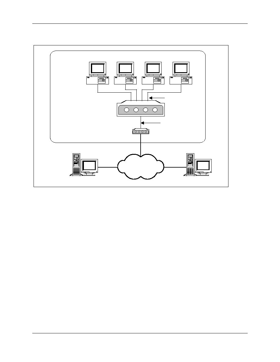
CX82100 Home Network Processor Data Sheet
101306C
Conexant Proprietary and Confidential Information
1-11
Figure 1-5. Example of a Residential Gateway Firewall plus Router Application
Broadband Access Device
Hom e PC
101306_069
Residential Gateway (RG)
Firew all Plus Router
using the CX82100 HNP
Ethernet (RJ45)
Ethernet
Network Server
Network Server
Public Networks
Hom e PC
Hom e PC
Home PC
RJ45
RJ45
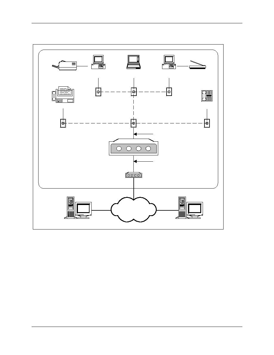
CX82100 Home Network Processor Data Sheet
1-12
Conexant Proprietary and Confidential Information
101306C
Figure 1-6. Example of a HomePNA 2.0 Bridge Application
RJ-11
101306_001
Ethernet
Hom ePNA 2.0
Hom e PNA 2.0 Bridge
using the CX82100 HNP
RJ-45
Phone
Fax
Hom ePNA 2.0
Phone Line Netw ork
Printer
Scanner
Hom e PC
Hom e PC
Laptop com puter
Network Server
Network Server
Public Networks
Broadband Access Device

CX82100 Home Network Processor Data Sheet
101306C
Conexant Proprietary and Confidential Information
1-13
1.6
References
[1]
ARM9TDMI Data Sheet, November, 1997, ARM Limited.
[2]
ARM940T Data Sheet, November, 1997, ARM Limited.
[3]
AMBA≠Advanced Microcontroller Bus Architecture Specification, April, 1997,
ARM Limited.
[4]
ANSI/IEEE 802.3, Reference Number ISO/IEC 8802-3, Part 3: Carrier Sense
Multiple Access with Collision detection (CSMA/CD) Access Method and
Physical Layer Specifications, Fifth Edition, 1996-07-29.
[5]
ANSI/IEEE 802.3u, Media Access Control (MAC) Parameters, Physical Layer,
Medium Attachment Units, and Repeater for 100 Mb/s Operation, Type 100Base-
T (Clauses 21-30), 1995.
[6]
PC SDRAM Specification, Revision 1.63, October 1998, Intel.
[7]
CX82110 xDSL Ready Home Network Processor (HNP) Data Sheet, Doc. No.
101545, Conexant.
[8]
CX24611 HomePNA 2.0 PHY/AFE Data Sheet, Doc. No. 100633, Conexant.

CX82100 Home Network Processor Data Sheet
1-14
Conexant Proprietary and Confidential Information
101306C
1.7
Key Words
7-WS or 7WS
7-Wire Serial Interface
AFE
Analog Front End
AMBA
Advanced Microprocessor Bus Architecture
APB
Advanced Peripheral Bus
ARM
Advanced Risk Microcontroller
ASB
Advanced System Bus
ASIC
Application Specific Integrated Circuit
CRC
Cyclic Redundancy Check
DMAC
Direct Memory Access Controller
EMAC
Ethernet Medium Access Control
EMC
External Memory Controller
FIFO
First-In-First-Out
GPIO
General Purpose I/O
GPSI
General Purpose Serial Interface
HomePNA
Home Phoneline Networking Alliance
HomePlug
HomePlug Power Line Alliance
ICE
In Circuit Emulator/Emulation
LSb
Least Significant Bit
LSB
Least Significant Byte
MAC
Media Access Control
MII
Media Independent Interface
MSb
Most Significant Bit
MSB
Most Significant Byte
OSI
Open Systems Interconnection
PHY
PHYsical Layer
SOHO
Small Office Home Office
STA
STAtion management entity
TIC
Test Interface Controller

CX82100 Home Network Processor Data Sheet
101306C
Conexant Proprietary and Confidential Information
1-15
1.8
Conventions
1.8.1
Data Lengths
qword
64-bits
dword
32-bits
word
16-bits
byte
8 bits
nibble
4 bits
1.8.2
Register Descriptions
Register Type
Description
RO
Read-only
WO
Write-only
RW
Read/Write
RW*
Read/Write, but data may not be same as written at a later time
RR
Same as RW, but writing a 1 resets corresponding bit location,
writing 0 has no effect
RWp
Read-only, Write-only shared port, data written cannot be
read. Only accessible by DMAC
Wd
Write-only, operates on other data entering register

CX82100 Home Network Processor Data Sheet
1-16
Conexant Proprietary and Confidential Information
101306C
This page is intentionally blank.

CX82100 Home Network Processor Data Sheet
101306C
Conexant Proprietary and Confidential Information
2-1
2
CX82100 HNP Hardware Interface
2.1
CX82100 HNP Hardware Interface Signals
2.1.1
CX82100-11/-12/-51/-52 Signal Interface and Pin Assignments
CX82100-11/-12/-51/-52 HNP hardware interface signals are shown in Figure 2-1.
CX82100-11/-12/-51/-52 HNP pin signals are shown in Figure 2-2 and are listed in Table
2-1.
Note:
The CX82100-11/-12/-51/-52 supports the following two signals on the indicated
pins (different from the CX82100-41/-42): P13 = VSS0 and P14 = HC00
(HCS0#)/GPIO32 (see Section 2.1.1). Other pinouts are the same as the
CX82100-41/-42.
2.1.2
CX82100-41/-42 Signal Interface and Pin Assignments
CX82100-41/-42 HNP hardware interface signals are shown in Figure 2-3.
CX82100-41/-42 HNP pin signals are shown in Figure 2-4 and are listed in Table 2-2.
Note:
The CX82100-41/-42 supports the following two signals on the indicated pins
(different from the CX82100-11/-12/-51/-52): P13 = HC00 (HCS0#)/GPIO32
and P14 = HC10 (HRDY#) (see Section 2.1.2). Other pinouts are the same as
the CX82100-11/-12/-51/-52.
2.1.3
CX82100 HNP Signal Definitions
CX82100 HNP hardware interface signals are defined in Table 2-3.
CX82100 HNP input/output types are described in Table 2-4.
CX82100 HNP DC electrical characteristics are listed in Table 2-5.
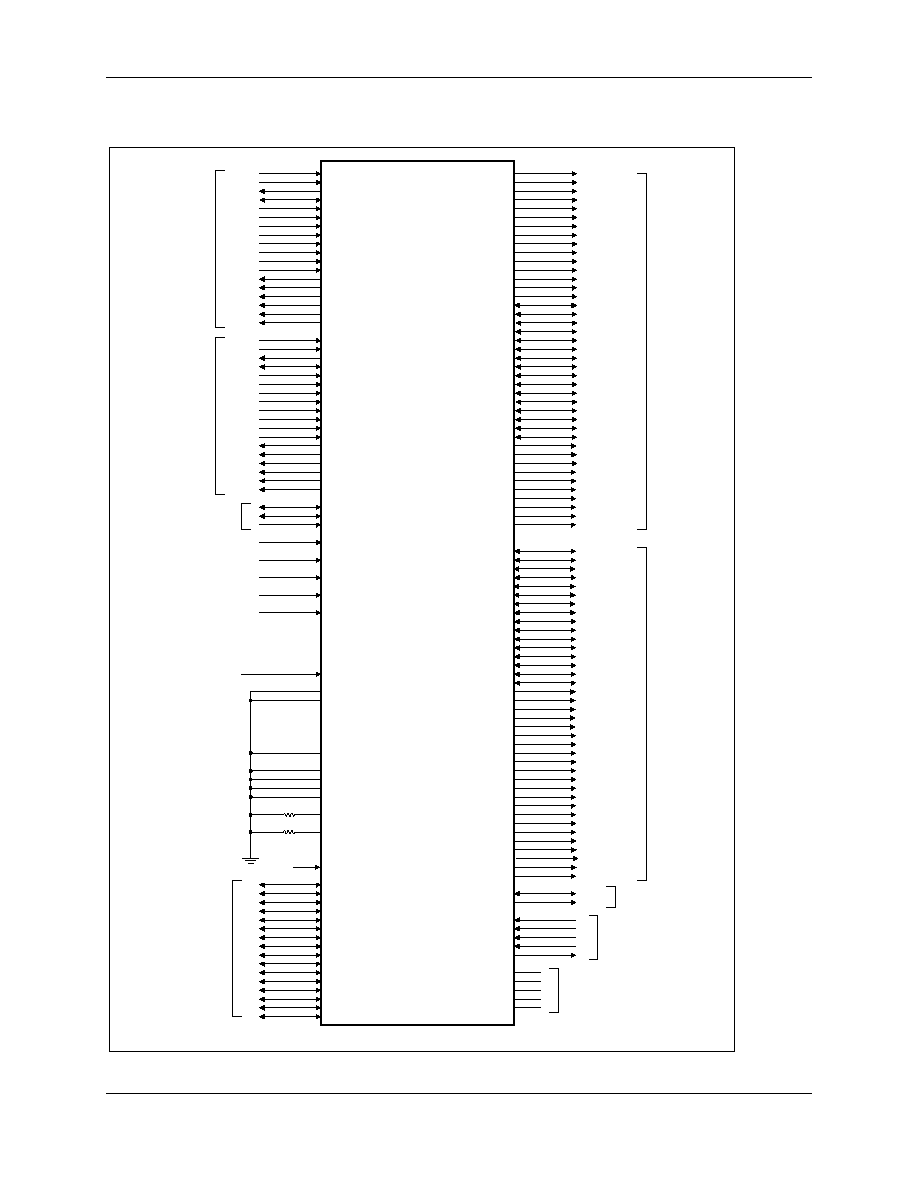
CX82100 Home Network Processor Data Sheet
2-2
Conexant Proprietary and Confidential Information
101306C
Figure 2-1. CX82100-11/-12/-51/-52 HNP Hardware Interface Signals
EM1_COL
EM1_CRS
EM1_MDC
EM1_MDIO
EM1_RX_CLK
EM1_RXD0
EM1_RXD1
EM1_RXD2
EM1_RXD3
EM1_RXDV
EM1_RXER
EM1_TX_CLK
EM1_TX_EN
EM1_TXD0
EM1_TXD1
EM1_TXD2
EM1_TXD3
EM1_TXER
EM2_COL
EM2_CRS
EM2_MDC
EM2_MDIO
EM2_RX_CLK
EM2_RXD0
EM2_RXD1
EM2_RXD2
EM2_RXD3
EM2_RXDV
EM2_RXER
EM2_TX_CLK
EM2_TX_EN
EM2_TXD0
EM2_TXD1
EM2_TXD2
EM2_TXD3
EM2_TXER
USBP
USBN
USB_PWR_DET (GPIO22)*
CLKI
HRST#
VGG
VDD
VDDA
VDDO
VSS
VSSA
VSSO
TST0
TST1
TST2
TST3
PLLBP
BOPT (GPIO14)*
TREQA
GPIO5
GPIO6
GPIO7
GPIO8
GPIO17
GPIO18
GPIO19
GPIO20
GPIO21
GPIO24
GPIO25
GPIO26
GPIO27
GPIO31
BCLKIO/GPIO38
FCLKIO/GPIO39
G1
G2
K8
M8
G5
H4
H3
H1
H2
L7
P8
E1
F1
F2
F5
F3
E4
G3
B8
J12
B6
A6
C8
A14
A7
B7
E7
C7
D7
L13
J13
M14
K12
L12
L14
K14
D9
E8
C9
J2
N14
H6
H7, H8
G6
A12, B3, B5,
D1, D14, F6,
F9, F12, H10,
J7, K7, K11,
N5, , N9, N11,
N13, P1
G7, G8
H5
A5, B9, B11, D8
D12, F4, G9, H11
K13, L2, N8, P2
P5, P9,
P11, P13, C4
C5
B4
A4
D4
J3
K4
K5
E6
D6
E5
D5
A3
A2
B2
B1
C3
A1
M7
A8
G4
C6
J5
J1
+3.3V
HAD00
HAD01
HAD02
HAD03
HAD04
HAD05
HAD06
HAD07
HAD08
HAD09
HAD10
HAD11
HAD12
HAD13
HAD14
HAD15
HC01
HC02
HC03
HC04
HC05
HC06
HC07
HAD16
HAD17
HAD18
HAD19
HAD20
HAD21
HAD22
HAD23
HAD24
HAD25
HAD26
HAD27
HAD28
HAD29
HC08 (HRD#)
HC09 (HWR#)
HC00 (HCS0#)/GPIO32
HAD31 (HCS4#)/GPIO37
MD00
MD01
MD02
MD03
MD04
MD05
MD06
MD07
MD08
MD09
MD10
MD11
MD12
MD13
MD14
MD15
MA00
MA01
MA02
MA03
MA04
MA05
MA06
MA07
MA08
MA09
MA10
MA11
MM0
MM1
MB0
MB1
MRAS#
MCAS#
MWE#
MCS#
MCLK
MCKE
I2C_DATA (GPIO15)**
I2C_CLOCK (GPIO16)**
TRST#
TCK
TMS
TDI
TDO
NC
NC
NC
NC
NC
P12
N12
L11
J10
M11
L10
K10
L9
M10
P10
N10
J9
K9
L8
M9
N7
P7
L6
P6
N6
K6
M6
L5
M5
L4
P4
N4
M4
P3
N3
M3
N1
N2
M1
M2
L1
L3
M13
M12
P14
J8
F11
E13
F10
F14
G11
F13
G10
G14
H9
G12
G13
H14
J11
H13
H12
J14
A10
B10
D10
C10
A11
F8
C11
D11
B12
A13
C12
B13
E11
E10
A9
E9
D13
C13
B14
C14
E14
E12
E2
E3
J4
K2
J6
K1
K3
C1
C2
D2
D3
F7
101306_066
CX82100
(-11/-12/-51/-52)
Home Network
Processor
(HNP)
196-Pin FPBGA
SDRAM
or
SRAM
MEDIA INDEPENDENT
INTERFACE 1 (MII 1)/
7-WIRE SERIAL
INTERFACE (7-WS1)
CLOCK
RESET CIRCUIT
JTAG
+3.3V OR +5V (CLAMP)
+1.8V
+1.8V (THROUGH FILTER)
PARALLEL
EXPANSION
BUS
D00
D01
D02
D03
D04
D05
D06
D07
D08
D09
D10
D11
D12
D13
D14
D15
A0
A1
A2
A3
A4
A5
A6
A7
A8
A9
A10
A11
A12
A13
A14
A15
A16
A17
A18
A19
A20
RD#
WE#
CS0# (Flash)
D0
D1
D2
D3
D4
D5
D6
D7
D8
D9
D10
D11
D12
D13
D14
D15
A0
A1
A2
A3
A4
A5
A6
A7
A8
A9
A10
A11
DQMH
DQML
BA0
BA1
RAS#
CAS#
WE#
CS#
CLKE
CLK
SDA
SCL
USB
INTERFACE
MEDIA INDEPENDENT
INTERFACE 2 (MII 2)/
7-WIRE SERIAL
INTERFACE (7-WS2)
Serial EEPROM
(Optional)
COL
CRS
MDC
MDIO
RX_CLK
RXD0
RXD1
RXD2
RXD3
RXDV
RXER
TX_CLK
TX_EN
TXD0
TXD1
TXD2
TXD3
TXER
COL
CRS
MDC
MDIO
RX_CLK
RXD0
RXD1
RXD2
RXD3
RXDV
RXER
TX_CLK
TX_EN
TXD0
TXD1
TXD2
TXD3
TXER
* Dedicated GPIO signal.
** May be assigned to different application use if not
used for indicated function.
NC
4.7K
4.7K
APPLICATION
DEPENDENT
NC
CX82100 Home Network Processor Data Sheet
101306C
Conexant Proprietary and Confidential Information
2-3
Figure 2-2. CX82100-11/-12/-51/-52 HNP Pin Signals-196-Pin FPBGA
A1
B1
C1
D1
E1
F1
G1
H1
J1
K1
L1
M1
N1
P1
1
2
3
4
5
6
7
8
9
10
11
12
13
14
A2
B2
C2
D2
E2
F2
G2
H2
J2
K2
L2
M2
N2
P2
A3
B3
C3
D3
E3
F3
G3
H3
J3
K3
L3
M3
N3
P3
A4
B4
C4
D4
E4
F4
G4
H4
J4
K4
L4
M4
N4
P4
A5
B5
C5
D5
E5
F5
G5
H5
J5
K5
L5
M5
N5
P5
A6
B6
C6
D6
E6
F6
G6
H6
J6
K6
L6
M6
N6
P6
A7
B7
C7
D7
E7
F7
G7
H7
J7
K7
L7
M7
N7
P7
A10
B10
C10
D10
E10
F10
G10
H10
J10
K10
L10
M10
N10
P10
A8
B8
C8
D8
E8
F8
G8
H8
J8
K8
L8
M8
N8
P8
A9
B9
C9
D9
E9
F9
G9
H9
J9
K9
L9
M9
N9
P9
A11
B11
C11
D11
E11
F11
G11
H11
J11
K11
L11
M11
N11
P11
A12
B12
C12
D12
E12
F12
G12
H12
J12
K12
L12
M12
N12
P12
A13
B13
C13
D13
E13
F13
G13
H13
J13
K13
L13
M13
N13
P13
A14
B14
C14
D14
E14
F14
G14
H14
J14
K14
L14
M14
N14
P14
A
B
C
D
E
F
G
H
J
K
L
M
N
P
GPIO24
GPIO20
NC
VDDO
EM1_TX_CLK
EM1_TX_EN
EM1_COL
EM1_RXD2
FCLKIO/GPIO39
TDI
HAD28
HAD26
HAD24
VDDO
GPIO18
GPIO19
NC
NC
I2C_DATA (GPIO15)
EM1_TXD0
EM1_CRS
EM1_RXD3
CLKI
TCK
VSSO
HAD27
HAD25
VSSO
TOP VIEW
101306_067
GPIO17
VDDO
GPIO21
NC
GPIO16
EM1_TXD2
EM1_TXER
EM1_RXD1
PLLBP
TDO
HAD29
HAD23
HAD22
HAD21
TST2
TST1
VSSO
TST3
EM1_TXD3
VSSO
GPIO27
EM1_RXD0
TRST#
BOPT (GPIO14)
HAD17
HAD20
HAD19
HAD18
VSSO
VDDO
TST0
GPIO8
GPIO7
EM1_TXD1
EM1_RX_CLK
VSSA
BCLKIO/GPIO38
TREQA
HC07
HAD16
VDDO
VSSO
EM2_MDIO
EM2_MDC
GPIO31
GPIO6
GPIO5
VDD0
VDDA
VGG
TMS
HC05
HC02
HC06
HC04
HC03
EM2_RXD1
EM2_RXD2
EM2_RXDV
EM2_RXER
EM2_RXD3
NC
VSS
VDD
VDDO
VDDO
EM1_RXDV
GPIO25
HAD15
HC01
GPIO26
EM2_COL
EM2_RX_CLK
VSSO
USBN
MA05
VSS
VDD
HAD31 (HCS4#)/GPIO37
EM1_MDC
HAD13
EM1_MDIO
VSS0
EM1_RXER
MB0
VSSO
USB_PWR_DET (GPIO22)
USBP
MB1
VDDO
VSSO
MD08
HAD11
HAD12
HAD07
HAD14
VDDO
VSSO
MA00
MA01
MA03
MA02
MM1
MD02
MD06
VDDO
HAD03
HAD06
HAD05
HAD08
HAD10
HAD09
MA04
VSSO
MA06
MA07
MM0
MD00
MD04
VSSO
MD12
VDDO
HAD02
HAD04
VDDO
VSSO
VDDO
MA08
MA10
VSSO
MCKE
VDDO
MD09
MD14
EM2_CRS
EM2_TXD1
EM2_TXD2
HC09 (HWR#)
HAD01
HAD00
MA09
MA11
MCAS#
MRAS#
MD01
MD05
MD10
MD13
EM2_TX_EN
VSSO
EM2_TX_CLK
HC08 (HRD#)
VDDO
VSSO
EM2_RXD0
MWE#
MCS#
VDDO
MCLK
MD03
MD07
MD11
MD15
EM2_TXER
EM2_TXD3
EM2_TXD0
HRST#
HC00 (HCS0#)/GPIO32

CX82100 Home Network Processor Data Sheet
2-4
Conexant Proprietary and Confidential Information
101306C
Table 2-1. CX82100-11/-12/-51/-52 HNP Pin Signals ≠ 196-Pin FPBGA
Pin
Signal
Pin
Signal
Pin
Signal
Pin
Signal
A1
GPIO24
D8
VSSO
H1
EM1_RXD2
L8
HAD13
A2
GPIO18
D9
USBP
H2
EM1_RXD3
L9
HAD07
A3
GPIO17
D10
MA02
H3
EM1_RXD1
L10
HAD05
A4
TST2
D11
MA07
H4
EM1_RXD0
L11
HAD02
A5
VSSO
D12
VSSO
H5
VSSA
L12
EM2_TXD2
A6
EM2_MDIO
D13
MRAS#
H6
VGG
L13
EM2_TX_CLK
A7
EM2_RXD1
D14
VDDO
H7
VDD
L14
EM2_TXD3
A8
GPIO26
E1
EM1_TX_CLK
H8
VDD
M1
HAD26
A9
MB0
E2
I2C_DATA (GPIO15)
H9
MD08
M2
HAD27
A10
MA00
E3
I2C_CLOCK (GPIO16)
H10
VDDO
M3
HAD23
A11
MA04
E4
EM1_TXD3
H11
VSSO
M4
HAD20
A12
VDDO
E5
GPIO7
H12
MD14
M5
HAD16
A13
MA09
E6
GPIO5
H13
MD13
M6
HC06
A14
EM2_RXD0
E7
EM2_RXD3
H14
MD11
M7
GPIO25
B1
GPIO20
E8
USBN
J1
FCLKIO/GPIO39
M8
EM1_MDIO
B2
GPIO19
E9
MB1
J2
CLKI
M9
HAD14
B3
VDDO
E10
MM1
J3
PLLBP
M10
HAD08
B4
TST1
E11
MM0
J4
TRST#
M11
HAD04
B5
VDDO
E12
MCKE
J5
BCLKIO/GPIO38
M12
HC09 (HWR#)
B6
EM2_MDC
E13
MD01
J6
TMS
M13
HC08 (HRD#)
B7
EM2_RXD2
E14
MCLK
J7
VDDO
M14
EM2_TXD0
B8
EM2_COL
F1
EM1_TX_EN
J8
HAD31 (HCS4#)/GPIO37
N1
HAD24
B9
VSSO
F2
EM1_TXD0
J9
HAD11
N2
HAD25
B10
MA01
F3
EM1_TXD2
J10
HAD03
N3
HAD22
B11
VSSO
F4
VSSO
J11
MD12
N4
HAD19
B12
MA08
F5
EM1_TXD1
J12
EM2_CRS
N5
VDDO
B13
MA11
F6
VDDO
J13
EM2_TX_EN
N6
HC04
B14
MWE#
F7
NC
J14
MD15
N7
HAD15
C1
NC
F8
MA05
K1
TDI
N8
VSSO
C2
NC
F9
VDDO
K2
TCK
N9
VDDO
C3
GPIO21
F10
MD02
K3
TDO
N10
HAD10
C4
VSSO
F11
MD00
K4
BOPT (GPIO14)
N11
VDDO
C5
TST0
F12
VDDO
K5
TREQA
N12
HAD01
C6
GPIO31
F13
MD05
K6
HC05
N13
VDDO*
C7
EM2_RXDV
F14
MD03
K7
VDDO
N14
HRST#
C8
EM2_RX_CLK
G1
EM1_COL
K8
EM1_MDC
P1
VDDO
C9
USB_PWR_DET (GPIO22)
G2
EM1_CRS
K9
HAD12
P2
VSSO
C10
MA03
G3
EM1_TXER
K10
HAD06
P3
HAD21
C11
MA06
G4
GPIO27
K11
VDDO
P4
HAD18
C12
MA10
G5
EM1_RX_CLK
K12
EM2_TXD1
P5
VSSO
C13
MCAS#
G6
VDDA
K13
VSSO
P6
HC03
C14
MCS#
G7
VSS
K14
EM2_TXER
P7
HC01
D1
VDDO
G8
VSS
L1
HAD28
P8
EM1_RXER
D2
NC
G9
VSSO
L2
VSSO
P9
VSSO
D3
NC
G10
MD06
L3
HAD29
P10
HAD09
D4
TST3
G11
MD04
L4
HAD17
P11
VSSO
D5
GPIO8
G12
MD09
L5
HC07
P12
HAD00
D6
GPIO6
G13
MD10
L6
HC02
P13
VSSO*
D7
EM2_RXER
G14
MD07
L7
EM1_RXDV
P14
HC00 (HCS0#)/GPIO32*
* Different from CX82100-41/-41.
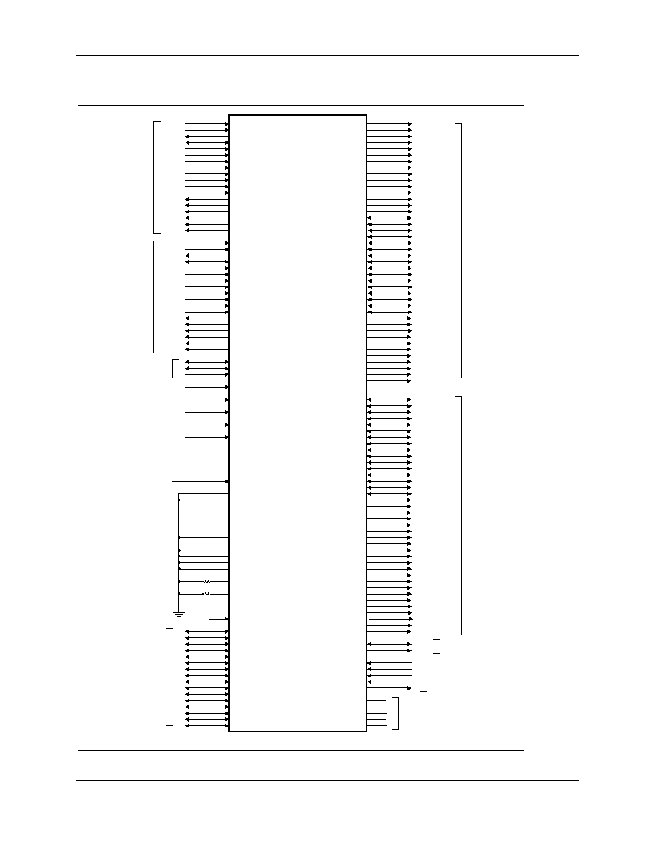
CX82100 Home Network Processor Data Sheet
101306C
Conexant Proprietary and Confidential Information
2-5
Figure 2-3. CX82100-41/-42 HNP Hardware Interface Signals
EM1_COL
EM1_CRS
EM1_MDC
EM1_MDIO
EM1_RX_CLK
EM1_RXD0
EM1_RXD1
EM1_RXD2
EM1_RXD3
EM1_RXDV
EM1_RXER
EM1_TX_CLK
EM1_TX_EN
EM1_TXD0
EM1_TXD1
EM1_TXD2
EM1_TXD3
EM1_TXER
EM2_COL
EM2_CRS
EM2_MDC
EM2_MDIO
EM2_RX_CLK
EM2_RXD0
EM2_RXD1
EM2_RXD2
EM2_RXD3
EM2_RXDV
EM2_RXER
EM2_TX_CLK
EM2_TX_EN
EM2_TXD0
EM2_TXD1
EM2_TXD2
EM2_TXD3
EM2_TXER
USBP
USBN
USB_PWR_DET (GPIO22)*
CLKI
HRST#
VGG
VDD
VDDA
VDDO
VSS
VSSA
VSSO
TST0
TST1
TST2
TST3
PLLBP
BOPT (GPIO14)*
TREQA
GPIO5
GPIO6
GPIO7
GPIO8
GPIO17
GPIO18
GPIO19
GPIO20
GPIO21
GPIO24
GPIO25
GPIO26
GPIO27
GPIO31
BCLKIO/GPIO38
FCLKIO/GPIO39
G1
G2
K8
M8
G5
H4
H3
H1
H2
L7
P8
E1
F1
F2
F5
F3
E4
G3
B8
J12
B6
A6
C8
A14
A7
B7
E7
C7
D7
L13
J13
M14
K12
L12
L14
K14
D9
E8
C9
J2
N14
H6
H7, H8
G6
A12, B3, B5,
D1, D14, F6,
F9, F12, H10,
J7, K7, K11,
N5, N9, N11, P1
G7, G8
H5
A5, B9, B11,
C4, D8, D12,
F4, G9, H11,
K13, L2, N8, N13,
P2, P5, P9, P11
C5
B4
A4
D4
J3
K4
K5
E6
D6
E5
D5
A3
A2
B2
B1
C3
A1
M7
A8
G4
C6
J5
J1
+3.3V
HAD00
HAD01
HAD02
HAD03
HAD04
HAD05
HAD06
HAD07
HAD08
HAD09
HAD10
HAD11
HAD12
HAD13
HAD14
HAD15
HC01
HC02
HC03
HC04
HC05
HC06
HC07
HAD16
HAD17
HAD18
HAD19
HAD20
HAD21
HAD22
HAD23
HAD24
HAD25
HAD26
HAD27
HAD28
HAD29
HC08 (HRD#)
HC09 (HWR#)
HC10 (HRDY#)
HC00 (HCS0#)/GPIO32
HAD31 (HCS4#)/GPIO37
MD00
MD01
MD02
MD03
MD04
MD05
MD06
MD07
MD08
MD09
MD10
MD11
MD12
MD13
MD14
MD15
MA00
MA01
MA02
MA03
MA04
MA05
MA06
MA07
MA08
MA09
MA10
MA11
MM0
MM1
MB0
MB1
MRAS#
MCAS#
MWE#
MCS#
MCLK
MCKE
I2C_DATA (GPIO15)**
I2C_CLOCK (GPIO16)**
TRST#
TCK
TMS
TDI
TDO
NC
NC
NC
NC
NC
P12
N12
L11
J10
M11
L10
K10
L9
M10
P10
N10
J9
K9
L8
M9
N7
P7
L6
P6
N6
K6
M6
L5
M5
L4
P4
N4
M4
P3
N3
M3
N1
N2
M1
M2
L1
L3
M13
M12
P14
P13
J8
F11
E13
F10
F14
G11
F13
G10
G14
H9
G12
G13
H14
J11
H13
H12
J14
A10
B10
D10
C10
A11
F8
C11
D11
B12
A13
C12
B13
E11
E10
A9
E9
D13
C13
B14
C14
E14
E12
E2
E3
J4
K2
J6
K1
K3
C1
C2
D2
D3
F7
101306_072
CX82100
(-41/-42)
Home Network
Processor
(HNP)
196-Pin FPBGA
SDRAM
or
SRAM
MEDIA INDEPENDENT
INTERFACE 1 (MII 1)/
7-WIRE SERIAL
INTERFACE (7-WS1)
CLOCK
RESET CIRCUIT
JTAG
+3.3V OR +5V (CLAMP)
+1.8V
+1.8V (THROUGH FILTER)
PARALLEL
EXPANSION
BUS
D00
D01
D02
D03
D04
D05
D06
D07
D08
D09
D10
D11
D12
D13
D14
D15
A0
A1
A2
A3
A4
A5
A6
A7
A8
A9
A10
A11
A12
A13
A14
A15
A16
A17
A18
A19
A20
RD#
WE#
CS0# (Flash)
D0
D1
D2
D3
D4
D5
D6
D7
D8
D9
D10
D11
D12
D13
D14
D15
A0
A1
A2
A3
A4
A5
A6
A7
A8
A9
A10
A11
DQMH
DQML
BA0
BA1
RAS#
CAS#
WE#
CS#
CLKE
CLK
SDA
SCL
USB
INTERFACE
MEDIA INDEPENDENT
INTERFACE 2 (MII 2)/
7-WIRE SERIAL
INTERFACE (7-WS2)
Serial EEPROM
(Optional)
COL
CRS
MDC
MDIO
RX_CLK
RXD0
RXD1
RXD2
RXD3
RXDV
RXER
TX_CLK
TX_EN
TXD0
TXD1
TXD2
TXD3
TXER
COL
CRS
MDC
MDIO
RX_CLK
RXD0
RXD1
RXD2
RXD3
RXDV
RXER
TX_CLK
TX_EN
TXD0
TXD1
TXD2
TXD3
TXER
* Dedicated GPIO signal.
** May be assigned to different application use if not
used for indicated function.
NC
4.7K
4.7K
APPLICATION
DEPENDENT
NC
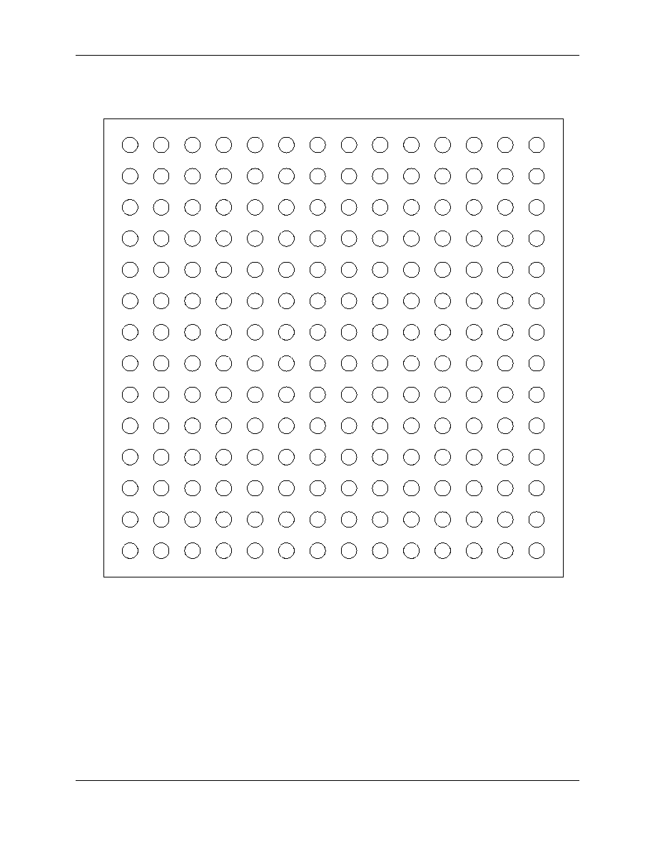
CX82100 Home Network Processor Data Sheet
2-6
Conexant Proprietary and Confidential Information
101306C
Figure 2-4. CX82100-41/-42 HNP Pin Signals-196-Pin FPBGA
A1
B1
C1
D1
E1
F1
G1
H1
J1
K1
L1
M1
N1
P1
1
2
3
4
5
6
7
8
9
10
11
12
13
14
A2
B2
C2
D2
E2
F2
G2
H2
J2
K2
L2
M2
N2
P2
A3
B3
C3
D3
E3
F3
G3
H3
J3
K3
L3
M3
N3
P3
A4
B4
C4
D4
E4
F4
G4
H4
J4
K4
L4
M4
N4
P4
A5
B5
C5
D5
E5
F5
G5
H5
J5
K5
L5
M5
N5
P5
A6
B6
C6
D6
E6
F6
G6
H6
J6
K6
L6
M6
N6
P6
A7
B7
C7
D7
E7
F7
G7
H7
J7
K7
L7
M7
N7
P7
A10
B10
C10
D10
E10
F10
G10
H10
J10
K10
L10
M10
N10
P10
A8
B8
C8
D8
E8
F8
G8
H8
J8
K8
L8
M8
N8
P8
A9
B9
C9
D9
E9
F9
G9
H9
J9
K9
L9
M9
N9
P9
A11
B11
C11
D11
E11
F11
G11
H11
J11
K11
L11
M11
N11
P11
A12
B12
C12
D12
E12
F12
G12
H12
J12
K12
L12
M12
N12
P12
A13
B13
C13
D13
E13
F13
G13
H13
J13
K13
L13
M13
N13
P13
A14
B14
C14
D14
E14
F14
G14
H14
J14
K14
L14
M14
N14
P14
A
B
C
D
E
F
G
H
J
K
L
M
N
P
GPIO24
GPIO20
NC
VDDO
EM1_TX_CLK
EM1_TX_EN
EM1_COL
EM1_RXD2
FCLKIO/GPIO39
TDI
HAD28
HAD26
HAD24
VDDO
GPIO18
GPIO19
NC
NC
I2C_DATA (GPIO15)
EM1_TXD0
EM1_CRS
EM1_RXD3
CLKI
TCK
VSSO
HAD27
HAD25
VSSO
TOP VIEW
101306_073
GPIO17
VDDO
GPIO21
NC
GPIO16
EM1_TXD2
EM1_TXER
EM1_RXD1
PLLBP
TDO
HAD29
HAD23
HAD22
HAD21
TST2
TST1
VSSO
TST3
EM1_TXD3
VSSO
GPIO27
EM1_RXD0
TRST#
BOPT (GPIO14)
HAD17
HAD20
HAD19
HAD18
VSSO
VDDO
TST0
GPIO8
GPIO7
EM1_TXD1
EM1_RX_CLK
VSSA
BCLKIO/GPIO38
TREQA
HC07
HAD16
VDDO
VSSO
EM2_MDIO
EM2_MDC
GPIO31
GPIO6
GPIO5
VDD0
VDDA
VGG
TMS
HC05
HC02
HC06
HC04
HC03
EM2_RXD1
EM2_RXD2
EM2_RXDV
EM2_RXER
EM2_RXD3
NC
VSS
VDD
VDDO
VDDO
EM1_RXDV
GPIO25
HAD15
HC01
GPIO26
EM2_COL
EM2_RX_CLK
VSSO
USBN
MA05
VSS
VDD
HAD31 (HCS4#)/GPIO37
EM1_MDC
HAD13
EM1_MDIO
VSS0
EM1_RXER
MB0
VSSO
USB_PWR_DET (GPIO22)
USBP
MB1
VDDO
VSSO
MD08
HAD11
HAD12
HAD07
HAD14
VDDO
VSSO
MA00
MA01
MA03
MA02
MM1
MD02
MD06
VDDO
HAD03
HAD06
HAD05
HAD08
HAD10
HAD09
MA04
VSSO
MA06
MA07
MM0
MD00
MD04
VSSO
MD12
VDDO
HAD02
HAD04
VDDO
VSSO
VDDO
MA08
MA10
VSSO
MCKE
VDDO
MD09
MD14
EM2_CRS
EM2_TXD1
EM2_TXD2
HC09 (HWR#)
HAD01
HAD00
MA09
MA11
MCAS#
MRAS#
MD01
MD05
MD10
MD13
EM2_TX_EN
VSSO
EM2_TX_CLK
HC08 (HRD#)
VSSO
HC00 (HCS0#)/GPIO32
EM2_RXD0
MWE#
MCS#
VDDO
MCLK
MD03
MD07
MD11
MD15
EM2_TXER
EM2_TXD3
EM2_TXD0
HRST#
HC10 (HRDY#)

CX82100 Home Network Processor Data Sheet
101306C
Conexant Proprietary and Confidential Information
2-7
Table 2-2. CX82100-41/-42 HNP Pin Signals ≠ 196-Pin FPBGA
Pin
Signal
Pin
Signal
Pin
Signal
Pin
Signal
A1
GPIO24
D8
VSSO
H1
EM1_RXD2
L8
HAD13
A2
GPIO18
D9
USBP
H2
EM1_RXD3
L9
HAD07
A3
GPIO17
D10
MA02
H3
EM1_RXD1
L10
HAD05
A4
TST2
D11
MA07
H4
EM1_RXD0
L11
HAD02
A5
VSSO
D12
VSSO
H5
VSSA
L12
EM2_TXD2
A6
EM2_MDIO
D13
MRAS#
H6
VGG
L13
EM2_TX_CLK
A7
EM2_RXD1
D14
VDDO
H7
VDD
L14
EM2_TXD3
A8
GPIO26
E1
EM1_TX_CLK
H8
VDD
M1
HAD26
A9
MB0
E2
I2C_DATA (GPIO15)
H9
MD08
M2
HAD27
A10
MA00
E3
I2C_CLOCK (GPIO16)
H10
VDDO
M3
HAD23
A11
MA04
E4
EM1_TXD3
H11
VSSO
M4
HAD20
A12
VDDO
E5
GPIO7
H12
MD14
M5
HAD16
A13
MA09
E6
GPIO5
H13
MD13
M6
HC06
A14
EM2_RXD0
E7
EM2_RXD3
H14
MD11
M7
GPIO25
B1
GPIO20
E8
USBN
J1
FCLKIO/GPIO39
M8
EM1_MDIO
B2
GPIO19
E9
MB1
J2
CLKI
M9
HAD14
B3
VDDO
E10
MM1
J3
PLLBP
M10
HAD08
B4
TST1
E11
MM0
J4
TRST#
M11
HAD04
B5
VDDO
E12
MCKE
J5
BCLKIO/GPIO38
M12
HC09 (HWR#)
B6
EM2_MDC
E13
MD01
J6
TMS
M13
HC08 (HRD#)
B7
EM2_RXD2
E14
MCLK
J7
VDDO
M14
EM2_TXD0
B8
EM2_COL
F1
EM1_TX_EN
J8
HAD31 (HCS4#)/GPIO37
N1
HAD24
B9
VSSO
F2
EM1_TXD0
J9
HAD11
N2
HAD25
B10
MA01
F3
EM1_TXD2
J10
HAD03
N3
HAD22
B11
VSSO
F4
VSSO
J11
MD12
N4
HAD19
B12
MA08
F5
EM1_TXD1
J12
EM2_CRS
N5
VDDO
B13
MA11
F6
VDDO
J13
EM2_TX_EN
N6
HC04
B14
MWE#
F7
NC
J14
MD15
N7
HAD15
C1
NC
F8
MA05
K1
TDI
N8
VSSO
C2
NC
F9
VDDO
K2
TCK
N9
VDDO
C3
GPIO21
F10
MD02
K3
TDO
N10
HAD10
C4
VSSO
F11
MD00
K4
BOPT (GPIO14)
N11
VDDO
C5
TST0
F12
VDDO
K5
TREQA
N12
HAD01
C6
GPIO31
F13
MD05
K6
HC05
N13
VSSO*
C7
EM2_RXDV
F14
MD03
K7
VDDO
N14
HRST#
C8
EM2_RX_CLK
G1
EM1_COL
K8
EM1_MDC
P1
VDDO
C9
USB_PWR_DET (GPIO22)
G2
EM1_CRS
K9
HAD12
P2
VSSO
C10
MA03
G3
EM1_TXER
K10
HAD06
P3
HAD21
C11
MA06
G4
GPIO27
K11
VDDO
P4
HAD18
C12
MA10
G5
EM1_RX_CLK
K12
EM2_TXD1
P5
VSSO
C13
MCAS#
G6
VDDA
K13
VSSO
P6
HC03
C14
MCS#
G7
VSS
K14
EM2_TXER
P7
HC01
D1
VDDO
G8
VSS
L1
HAD28
P8
EM1_RXER
D2
NC
G9
VSSO
L2
VSSO
P9
VSSO
D3
NC
G10
MD06
L3
HAD29
P10
HAD09
D4
TST3
G11
MD04
L4
HAD17
P11
VSSO
D5
GPIO8
G12
MD09
L5
HC07
P12
HAD00
D6
GPIO6
G13
MD10
L6
HC02
P13
HC00 (HCS0#)/GPIO32*
D7
EM2_RXER
G14
MD07
L7
EM1_RXDV
P14
HC10 (HRDY#)
* Different from CX82100-11/-12/-51/-52.
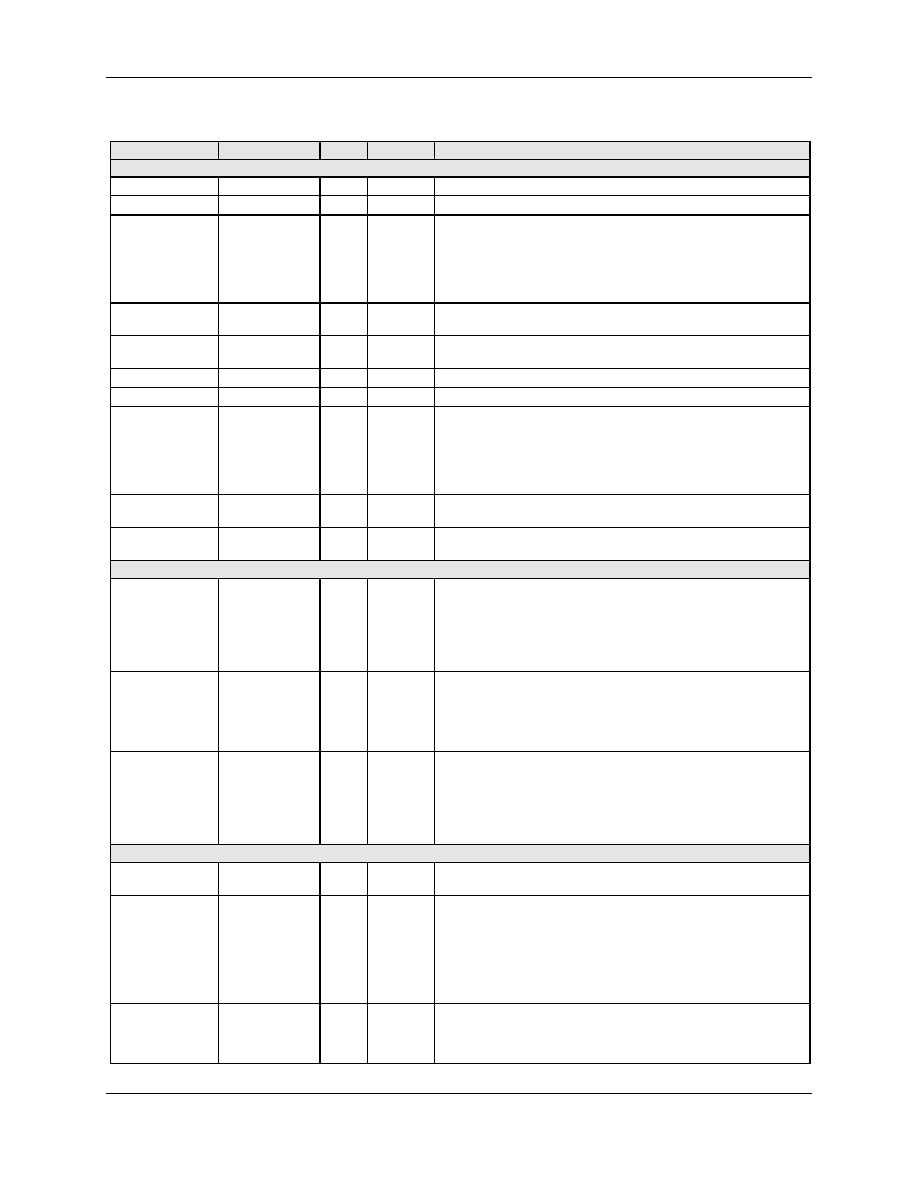
CX82100 Home Network Processor Data Sheet
2-8
Conexant Proprietary and Confidential Information
101306C
Table 2-3. CX82100 HNP Pin Signal Definitions
Pin Signal
Pin No.
I/O
I/O Type
Signal Name/Description
Power and Ground
VDD
H7, H8
P
PWR
Core Supply Voltage. Connect to +1.8V.
VDDA
G6
P
PWR
Supply Voltage. Connect to +1.8V through filter.
VDDO
A12, B3, B5,
D1, D14, F6,
F9, F12, H10,
J7, K7, K11,
N5, N9, N11,
P1
P
PWR
I/O Supply Voltage. Connect to +3.3V.
VDDO
N13 (CX82100
-11/-12/-51/-52)
P
PWR
I/O Supply Voltage. Connect to +3.3V.
VGG
H6
R
REF
I/O Clamp Power Supply. Connect to +5V if available, otherwise
connect to +3.3V.
VSS
G7, G8
G
GND
Core Ground. Connect to digital ground.
VSSA
H5
G
GND
Ground. Connect to digital ground.
VSSO
A5, B9, B11,
C4, D8, D12,
F4, G9, H11,
K13, L2, N8,
P2, P5, P9,
P11
G
GND
I/O Ground. Connect to digital ground.
VSSO
N13 (CX82100
≠41/-42)
G
GND
I/O Ground. Connect to digital ground.
VSSO
P13 (CX82100
-11/-12/-51/-52)
G
GND
I/O Ground. Connect to digital ground.
System Control
HRST#
N14
I
Ith
Reset. Active low input asserted for at least 100
µs to reset the
HNP. All hardware registers are initialized to their default state.
Upon de-assertion of HRST#, the HNP executes the Boot Loader
code (see BOPT pin) then starts processing of the application
code.
Connect HRST# to a reset circuit.
BOPT (GPIO14)
K4
I/O
Itpu/Ot4
Boot Loader Option. Upon de-assertion of the HRST# signal, the
Boot Loader code executes from internal ROM (BOPT pin high, i.e.,
open) or Flash ROM (BOPT pin low, i.e., connected to GND).
For normal operation, typically connect BOPT to GND through
4.7 k
to execute Boot Loader from Flash ROM.
PLLBP
J3
I
Itpd
PLL Bypass Mode Select. If the PLLBP pin is high (test mode),
pins FCLKIO and BCLKIO are FCLKIO and BCLKIO inputs only
(i.e., not GPIO pins). If the PLLBP pin is low (normal operation),
pins FCLKIO and BCLKIO operate as FCLKIO/GPIO39 and
BCLKIO/GPIO38 as selected in the GPIO_OPT register).
For normal operation, connect PLLBP to GND through 4.7 k
.
Clock Interface
CLKI
J2
I
Ith
Clock In. Connect to 35.328 MHz voltage controlled crystal
oscillator (VCXO) output through 51
.
BCLKIO/GPIO38
J5
I/O
Itpu/Ot4
Bit Clock I/O. If PLLBP pin is high (test mode), this pin is BCLKIO
input only (i.e., not GPIO38). If the PLLBP pin is low (normal
operation), this pin can be used as GPIO38 or BCLKIO (see
GPIO_OPT register bit 6 and PLLBP pin).
For normal operation, BCLKIO output supplies the 25 MHz to the
LAN1 and LAN2 interfaces. Connect BCLKIO to the LAN 1 X1 pin
and to the LAN2 X1 pin though a single 51
resistor.
FCLKIO/GPIO39
J1
I/O
Itpu/Ot4
Frame Clock I/O. If the PLLBP pin is high (test mode), this pin is
FCLKIO input only (i.e., not GPIO39). If the PLLBP pin is low
(normal operation), this pin can be used as GPIO39 or FCLKIO
(see GPIO_OPT register bit 7 and PLLBP pin).
CX82100 Home Network Processor Data Sheet
101306C
Conexant Proprietary and Confidential Information
2-9
Table 2-3. CX82100 HNP Pin Signal Definitions (Continued)
Pin Signal
Pin No.
I/O
I/O Type
Signal Name/Description
USB Interface
USBP
USBN
D9
E8
I/O
Iu/Ou
USB Port. USBP and USBN are the differential data positive and
negative signals of the USB port. Connect USBP and USBN to
USB +Data and -Data, respectively, through 24
, and optionally
through a quick switch in order to isolate the USBP and USBN from
the USB during suspend mode.
USB_PWR_DET
(GPIO22)
C9
I
It/Ot4
USB Power Detect. Active high input used to detect presence of
+5 V at the USB connector.
JTAG Interface
TRST#
J4
I
Itpu
JTAG Reset. A high-to-low transition on this signal forces the TAP
controller into a logic reset state. This pin has an internal pullup.
Leave open for normal operation.
TCK
K2
I
Itpu
JTAG Test Clock. This is the boundary scan clock input signal.
This pin has an internal pullup.
Leave open for normal operation.
TMS
J6
I
Itpu
JTAG Test Mode Select. This signal controls the operation of the
TAP controller. This pin has an internal pull-up.
Leave open for normal operation.
TDI
K1
I
Itpu
JTAG Test Input. This signal contains serial data that is shifted in
on the rising edge of TCK. The pin has an internal pullup.
Leave open for normal operation.
TDO
K3
O
Otts4
JTAG Test Output Data. This is the three-stateable boundary scan
data output signal from the MCU, and it is shifted out on the falling
edge of TCK.
Leave open for normal operation.
Test Interface Controller (TIC) [Factory Test Only]
TREQA
K5
I
Itpd
Reserved. This pin is connected to internal circuitry. Leave open.

CX82100 Home Network Processor Data Sheet
2-10
Conexant Proprietary and Confidential Information
101306C
Table 2-3. CX82100 HNP Pin Signal Definitions (Continued)
Pin Signal
Pin No.
I/O
I/O Type
Signal Name/Description
EMAC 1 Interface
EM1_COL
G1
I
Itpd
LAN 1 Collision Indication. In full-duplex mode, EM1_COL is
ignored. In half-duplex mode, EM1_COL is asserted by the LAN 1
EPHY upon detection of a collision on the medium, and remains
asserted while the collision condition persists.
For MII, connect to LAN 1 EPHY COL pin through 51
.
For 7-WS interface, connect to LAN 1 EPHY COL pin through
51
.
EM1_CRS
G2
I
Itpd
LAN 1 Carrier Sense. In full-duplex mode, EM1_CRS is ignored.
In half-duplex mode, EM1_CRS is asserted by the LAN 1 EPHY
when either the transmit or receive medium is not idle. It is de-
asserted by the LAN 1 EPHY when both the transmit and receive
media are idle. The LAN 1 EPHY ensures that EM1_CRS remains
asserted throughout the duration of a collision condition, i.e., when
EM1_COL = 1.
For MII, connect to LAN 1 EPHY CRS pin through 51
.
For 7-WS interface, connect to LAN 1 EPHY CRS pin through
51
.
EM1_MDC
K8
O
Otts4
LAN 1 Management Data Clock. EM1_MDC is sourced by the
Station Management entity (STA) of the EMAC as the timing
reference for transfer of information on the EM1_MDIO signal.
EM1_MDC is aperiodic and has no maximum high or low times.
The minimum high and low time for EM1_MDC is 160 ns each. The
minimum period for EM1_MDC is 400 ns.
For MII, connect to LAN 1 EPHY COL pin.
For 7-WS interface, leave open (not used).
EM1_MDIO
M8
I/O
Itpd/Ot4
LAN 1 Serial Management Data Input/Output. EM1_MDIO is a
bidirectional signal used to transfer control and status information
between the LAN 1 EPHY and the STA in the EMAC.
For MII, connect to LAN 1 EPHY MDIO pin and to +3.3V through
4.7 K
.
For 7-WS interface, connect to LAN 1 EPHY MDIO pin and to
+3.3V through 4.7 K
.
EM1_RX_CLK
G5
I
Itpd
LAN 1 Receive Clock. A 10 MHz square wave synchronized to the
Receive Data and only active while receiving an input bit stream.
EM1_RX_CLK is sourced by the LAN 1 EPHY. It provides the
timing reference for the transfer of EM1_RXDV, EM1_RXD[3:0],
and EM1_RXER signals from LAN 1 EPHY. The LAN 1 EPHY can
either recover EM1_RX_CLK from the received data or it may
derive EM1_RX_CLK from a nominal clock (e. g., the
EM1_TX_CLK reference). If loss of received signal from the
medium causes the LAN 1 EPHY to lose the recovered clock
reference, the LAN 1 EPHY must source the clock from a nominal
clock reference. Transitions from nominal clock to recovered clock
or vice versa are made only when EM1_RXDV is de-asserted.
During the interval between the assertion of EM1_CRS and the
assertion of EM1_RXDV at the beginning of a frame, the LAN 1
EPHY may extend a cycle of EM1_RX_CLK by holding it either
high or low until the LAN 1 EPHY has locked to the recovered
clock. Following the de-assertion of EM1_RXDV at the end of a
frame, the LAN 1 EPHY may extend a cycle of EM1_RX_CLK by
holding it either high or low for an interval not to exceed twice the
nominal clock period.
For MII, connect to LAN 1 EPHY RX_CLK pin 51
.
For 7-WS interface, connect to LAN 1 EPHY RX_CLK pin 51
.

CX82100 Home Network Processor Data Sheet
101306C
Conexant Proprietary and Confidential Information
2-11
Table 2-3. CX82100 HNP Pin Signal Definitions (Continued)
Pin Signal
Pin No.
I/O
I/O Type
Signal Name/Description
EM1_RXD[3:0]
H2, H1, H3, H4
I
Itpd
LAN 1 Receive Data. For MII interface, EM1_RXD[3:0] are the 4-
bit parallel receive data lines. Connect EM1_RXD[3:0] to LAN 1
PHY RXD[3:0] through 51
.
For 7-WS interface, EM1_RXD3 is the Receive input bit stream.
Connect EM1_RXD3 to LAN 1 EPHY RXD pin through 51
.
EM1_RXD[2:0] are not used and should be left open.
EM1_RXDV
L7
I
Itpd
LAN 1 Receive Data Valid. EM1_RXDV is asserted by the LAN 1
EPHY to indicate that the nibble on EM1_RXD[3:0] is valid. It
remains asserted for the received frame duration with the exception
of the preamble. It may or may not be asserted during the
preamble. EM1_RXDV is de-asserted prior to the first
EM1_RX_CLK period that follows the final nibble of a received
frame. When EM1_RXDV is de-asserted, the EMAC ignores
EM1_RXD[3:0].
For MII, connect to LAN 1 EPHY RX_DV pin through 51
.
For 7-WS interface, leave open (not used).
EM1_RXER
P8
I
Itpd
LAN 1 Receive Error. EM1_RXER is driven by the LAN 1 EPHY. It
is asserted for one or more EM1_RX_CLK periods to indicate that
an error was detected somewhere in the frame presently being
transferred from the LAN 1 EPHY. The RMAC hardware will detect
this condition and declare such a frame invalid. While EM1_RXDV
is deasserted, EM1_RXER has no effect on the Reconciliation
sublayer (which lies between the MII and the MAC), therefore, it
has no effect on the MAC as well.
For MII, connect to LAN 1 EPHY RX_RXER pin through 51
.
For 7-WS interface, leave open (not used).
EM1_TX_CLK
E1
I
Itpd
Transmit Clock. EM1_TX_CLK is sourced by the LAN 1 EPHY. It
provides the timing reference for the transfer of EM1_TX_EN,
EM1_TXD[3:0], and EM1_TXER signals to LAN 1 EPHY.
For MII, connect to LAN 1 EPHY TX_CLK pin through 51
.
For 7-WS interface, connect to LAN PHY TX_CLK pin through
51
.
EM1_TX_EN
F1
O
Otts4
LAN 1 Transmit Enable. EM1_TX_EN is driven off the rising edge
and sampled on the rising edge of EM1_TX_CLK. It indicates that
the HNP is presenting nibbles on the MII for transmission.
EM1_TX_EN is asserted when the HNP has data to transmit over
the medium and remains asserted for the duration of the entire
transmitted frame. The HNP de-asserts EM1_TX_EN prior to the
rising edge of EM1_TX_CLK following the final nibble of a frame.
For MII, connect to LAN 1 EPHY TX_EN pin.
For 7-WS interface, connect to LAN 1 EPHY TX_EN pin.
EM1_TXD[3:0]
E4, F3, F5, F2
O
Otts4
LAN 1 Transmit Data. For MII interface, EM1_TXD[3:0] are the 4-
bit parallel transmit data lines. EM1_TXD[3:0] is driven off the rising
edge and sampled on the rising edge of EM1_TX_CLK. The entire
transmitted frame data is presented by the EM1_TXD[3:0] signal
lines, and commences on the first leading edge of EM1_TX_CLK
subsequent to EM1_TX_EN assertion. For each EM1_TX_CLK
period in which EM1_TX_EN is asserted, EM1_TXD[3:0] are
accepted for transmission by the LAN 1 EPHY. All fields except for
the FCS are transmitted with the least significant nibble first. The
LSb of each nibble is placed on EM1_TXD0. Connect
EM1_TXD[3:0] to LAN 1 EPHY TXD[3:0] through 51
.
For 7-WS interface, EM1_TXD3 is the transmit input bit stream.
Connect EM1_TXD3 to LAN 1 EPHY TXD pin. EM1_TXD[2:0] are
not used and should be left open.
CX82100 Home Network Processor Data Sheet
2-12
Conexant Proprietary and Confidential Information
101306C
Table 2-3. CX82100 HNP Pin Signal Definitions (Continued)
Pin Signal
Pin No.
I/O
I/O Type
Signal Name/Description
EM1_TXER
G3
O
Otts4
LAN 1 Transmit Coding Error. When EM1_TXER is asserted for
one or more EM1_TX_CLK periods while EM1_TX_EN is also
asserted, the LAN 1 EPHY emits one or more symbols that are not
part of the valid data or delimiter set somewhere in the frame being
transmitted. Permissible encoding of EM1_TXER with EM1_TX_EN
and EM1_TXD[3:0] are:
EM1_TX_EN EM1_TXER EM1_TXD[3:0]
Description
0
0
0000≠1111 Normal Inter-Frame
0
1
0000≠1111 Reserved
1
0
0000≠1111 Normal Data
Transmission
1
1
0000≠1111 Transmit Error
Propagation
For MII, connect to LAN 1 EPHY TXER pin.
For 7-WS interface, leave open.
EMAC 2 Interface
The EMAC 2 interface is the same as the EMAC 1 interface. Refer to the EMAC1 interface for signal definitions.
EM2_COL
B8
I
Itpd
LAN 2 Collision Indication.
EM2_CRS
J12
I
Itpd
LAN 2 Carrier Sense.
EM2_MDC
B6
O
Otts4
LAN 2 Management Data Clock.
EM2_MDIO
A6
I/O
Itpd/Ot4
LAN 2 Serial Management Data Input/Output.
EM2_RX_CLK
C8
I
Itpd
LAN 2 Receive Clock.
EM2_RXD[3:0]
E7, B7, A7,
A14
I
Itpd
LAN 2 Receive Data.
EM2_RXDV
C7
I
Itpd
LAN 2 Receive Data Valid.
EM2_RXER
D7
I
Itpd
LAN 2 Receive Error
EM2_TX_CLK
L13
I
Itpd
LAN 2 Transmit Clock.
EM2_TX_EN
J13
O
Otts4
LAN 2 Transmit Enable.
EM2_TXD[3:0]
L14, L12, K12,
M14
O
Otts4
LAN 2 Transmit Data.
EM2_TXER
K14
O
Otts4
LAN 2 Transmit Error.
CX82100 Home Network Processor Data Sheet
101306C
Conexant Proprietary and Confidential Information
2-13
Table 2-3. CX82100 HNP Pin Signal Definitions (Continued)
Pin Signal
Pin No.
I/O
I/O Type
Signal Name/Description
Host Parallel Expansion Bus Interface
HAD[15:0]
N7, M9, L8, K9,
J9, N10, P10,
M10, L9, K10,
L10, M11, J10,
L11, N12, P12
I/O
Itpu/Ot4
Data Lines 15-00.
Typically, connect to Flash ROM D[15:0], respectively.
HAD[29:16]
L3, L1, M2, M1,
N2, N1, M3,
N3, P3, M4,
N4, P4, L4, M5
O
It/Ot4
Address Lines 20-7.
Typically, connect to Flash ROM A[20:10], respectively.
HC[07:01]
L5, M6, K6, N6,
P6, L6, P7
O
It/Ot4
Address Lines 6-0.
Typically, connect to Flash ROM A[6:0], respectively.
HC08 (HRD#)
M13
O
It/Ot4
Read Enable. Active low read enable asserted when data is
transferred from the selected device onto the data bus.
Typically, connect through 51
as HRD# to Flash ROM OE# and
through 51
as HRDUA# to UART OE#.
HC09 (HWR#)
M12
O
It/Ot4
Write Enable. Active low write enable asserted when data is
transferred from the data bus into the selected device.
Typically, connect through 51
as HWR# to Flash ROM WR# and
through 51
as HWRUA# to UART WR#.
HC00 (HCS0#)/
GPIO32
P14 (CX82100
-11/-12/-51/-51)
P13 (CX82100
-41/-42)
O
It/Ot4
Flash ROM Chip Enable. Active low output enables optional Flash
ROM when asserted.
Connect to Flash ROM CE#.
HC10 (HRDY#)
P14 (CX82100
-41/-42)
I
Itpd/Ot4
Application Dependent.
HAD31
(HCS4#)/
GPIO37
J8
O
It/Ot4
Application Dependent.
Serial EEPROM Interface
I2C_DATA
(GPIO15)
E2
I/O
Itpu/Ot4
Serial EEPROM Data. I2C_DATA is a bidirectional data line used
to transfer data into and out of the EEPROM.
Connect to the
EEPROM SDA pin and to +3.3V through 4.7K
.
I2C_CLOCK
(GPIO16)
E3
O
Itpu/Ot4
Serial EEPROM Shift Clock. The I2C_CLOCK output is used to
clock all data into and out of the EEPROM. Connect to the
EEPROM SCL pin and to +3.3V through 4.7K
.

CX82100 Home Network Processor Data Sheet
2-14
Conexant Proprietary and Confidential Information
101306C
Table 2-3. CX82100 HNP Pin Signal Definitions (Continued)
Pin Signal
Pin No.
I/O
I/O Type
Signal Name/Description
SDRAM/SRAM Interface
MA[11:00]
B13, C12, A13,
B12, D11, C11,
F8, A11, C10,
D10, B10, A10
O
Ot4
SDRAM/SRAM Address Lines. Twelve-bit multiplexed row and
column address bus addresses up to 8 MB of data.
Connect to SDRAM/SRAM A[11:0], respectively, through 51
.
MD[15:00]
J14, H12, H13,
J11, H14, G13,
G12, H9, G14,
G10, F13, G11,
F14, F10, E13,
F11
I/O
Itpu/Ot4
SDRAM/SRAM Data Lines. Sixteen-bit bidirectional data bus.
Connect to SDRAM/SRAM D[15:0], respectively, through 51
.
MM0
E11
O
Ot4
SDRAM Input/Output Mask 0/SRAM A12.
For SDRAM interface, this signal is a mask for write access.
Connect to SDRAM I/O Mask Low input through 51
.
For SRAM interface, this signal is address A12 output, Connect to
SRAM A12 input through 51
.
MM1
E10
O
Ot4
SDRAM Input/Output Mask 1/SRAM A13.
For SDRAM interface, this signal is a mask for write access.
Connect to SDRAM I/O Mask High input through 51
.
For SRAM interface, this signal is address A13 output. Connect to
SRAM A13 input through 51
.
MB0
A9
O
Ot4
SDRAM Bank Address Select 0/SRAM A14.
For SDRAM interface, this signal selects the active bank. Connect
to SDRAM/SRAM Bank Address Select 0 input through 51
for 8
MB SDRAM; leave open for 2 MB SDRAM.
For SRAM interface, this signal is address A14 output. Connect to
SRAM A14 input through 51
.
MB1
E9
O
Ot4
SDRAM Bank Address Select 1/SRAM A15.
For SDRAM interface, this signal selects the active bank. Connect
to SDRAM/SRAM Bank Address Select 1 input through 51
.
For SRAM interface, this signal is address A15 output. Connect to
SRAM A15 input through 51
.
MCS#
C14
O
Ot4
SDRAM Memory Chip Select/SRAM 2 Chip Enable.
For SDRAM interface, this active low output enables the SDRAM
command decoder. Connect to SDRAM CS# input through 51
.
For SRAM interface, this active low output enables SRAM 2. If one
SRAM is used, leave open; if two SRAMs are used, connect to
SRAM 2 CE# input through 51
.
MRAS#
D13
O
Ot4
SDRAM Row Address Strobe/SRAM 1 Chip Enable.
For SDRAM interface, this active low output starts SDRAM access
with strobe of row address. Connect to SDRAM RAS# input
through 51
.
For SRAM interface, this active low output enables SRAM 1. If one
SRAM is used, connect to SRAM CE# input; if two SRAMs are
used, connect to SRAM 1 CE# input through 51
.
MCAS#
C13
O
Ot4
SDRAM Column Address Strobe/SRAM A16.
For SDRAM interface, this active low output strobes column
address and data bytes. Connect to SDRAM CAS# input through
51
.
For SRAM interface, this signal is address A16 output. Connect to
SRAM A16 input through 51
.
CX82100 Home Network Processor Data Sheet
101306C
Conexant Proprietary and Confidential Information
2-15
Table 2-3. CX82100 HNP Pin Signal Definitions (Continued)
Pin Signal
Pin No.
I/O
I/O Type
Signal Name/Description
SDRAM/SRAM Interface (Continued)
MWE#
B14
O
Ot4
SDRAM/SRAM Memory Write Enable. This active low output
enables write access to SDRAM/SRAM. Connect to SDRAM/SRAM
WE# input through 51
.
MCKE
E12
O
Ot4
SDRAM Clock Enable/SRAM A17.
For SDRAM interface, this active high output enables the SDRAM
clock. Connect to SDRAM CLKE input through 51
.
For SRAM interface, this signal is address A17 output. Connect to
SRAM A17 input through 51
.
MCLK
E14
O
Ot4
SDRAM Clock.
For SDRAM interface, this signal supplies the clock to the SDRAM.
Connect to SDRAM CLK input through 51
. All SDRAM signals
are sampled on the positive (rising) edge.
For SRAM interface, this pin not used. Leave open.
General Purpose Input/Output (GPIO)
Recommended GPIO usage is listed in Table 2-9.
GPIO31
C6
I/O
Itpu/Ot4
Application Dependent. Reset state = Z(pu).
GPIO27
G4
I/O
Itpu/Ot4
Application Dependent. Reset state = Z(pu).
GPIO26
A8
I/O
Itpu/Ot4
Application Dependent. Reset state = Z(pu).
GPIO24
A1
I/O
Itpu/Ot4
Application Dependent. Reset state = Z(pu).
GPIO21
C3
I/O
Itpu/Ot4
Application Dependent. Reset state = Z(pu).
GPIO20
B1
I/O
Itpu/Ot4
Application Dependent. Reset state = Z(pu).
GPIO19
B2
I/O
Itpu/Ot4
Application Dependent. Reset state = Z(pu).
GPIO18
A2
I/O
Itpu/Ot4
Application Dependent. Reset state = Z(pu).
GPIO17
A3
I/O
Itpu/Ot4
Application Dependent. Reset state = low.
GPIO8
D5
I/O
Itpu/Ot4
Application Dependent. Reset state = low.
GPIO7
E5
O
Itpu/Ot4
Application Dependent. Reset state = Z(pu).
GPIO6
D6
O
Itpu/Ot4
Application Dependent. Reset state = Z(pu).
GPIO5
E6
O
Itpu/Ot4
Application Dependent. Reset state = Z(pu).
Test
TST[3:0]
D4, A4, B4, C5
Test Pins. Test configuration pins used only during the
manufacturing/test process.
For normal operation, connect TST[3:0] to ground.
No Connect Pins (Balls)
NC
C1, C2, D2, D3,
F7
No Connect. These pins (solder balls) are not connected to
internal circuitry. Leave open.
Notes:
1. I/O Types: See Table 2-4.
2. Unless otherwise specified, output pins or input pins with internal pulldowns or pullups can be left open if not used.
3. The Reset State notation indicates the state of the pin upon power-on and whether or not it has an internal pullup. Z means
a high impedance state (an input) and pu/pd means the pin has an internal pullup/pulldown.

CX82100 Home Network Processor Data Sheet
2-16
Conexant Proprietary and Confidential Information
101306C
Table 2-4. CX82100 HNP Input/Output Type Descriptions
I/O Type
Description
It
Digital input, +5V tolerant, CIN = 8 pF
It/Ot4
Digital input, +5V tolerant, CIN = 8 pF/Digital output, 4 mA, ZINT = 80
Ith
Digital input, +5V tolerant, with hysteresis, CIN = 8 pF
Ithpd
Digital input, +5V tolerant, with hysteresis, 75k
pull-down, CIN = 8 pF
Itpd
Digital input, +5V tolerant, 75k
pull-down, CIN = 8 pF
Itpu
Digital input, +5V tolerant, 75k
pull-up, CIN = 8 pF
Itpu/Ot4
Digital input, +5V tolerant, 75k
pull-up, CIN = 8 pF/Digital output, 4 mA, ZINT = 80
Otts4
Digital output, 3-State, 4 mA, ZINT =80
Iu/Ou
Input, USB receiver/Output, USB driver
Notes:
See DC characteristics in Table 2-5.
I/O Type corresponds to the device Pad Type. The I/O column in tables refers to signal I/O direction used in the application.
CX82100 Home Network Processor Data Sheet
101306C
Conexant Proprietary and Confidential Information
2-17
2.2
CX82100 HNP Electrical and Environmental Specifications
2.2.1
DC Electrical Characteristics
CX82100 HNP DC electrical characteristics are listed in Table 2-5.
Table 2-5. CX82100 HNP DC Electrical Characteristics
Parameter
Symbol
Min.
Typ.
Max.
Units
Test Conditions1
Input high voltage
VIH
2.0
VGG + 0.5
VDC
Input low voltage
VIL
-0.5
0.8
VDC
Input leakage current
IIL/IIH
µA
VIN = 0 for Min.
VIN = VIN (MAX) for Max.
Input leakage current (with internal pull-
downs) 2
IIL/IIH
µA
VIN = 0 for Min.
VIN = VIN (MAX) for Max.
Input leakage current (with internal pull-
ups) 2
IIL/IIH
µA
VIN = 0 for Min.
VIN = VIN (MAX) for Max.
Internal pullup/pulldown resistance
Rpu/Rpd
50
200
k
Output high voltage
VOH
2.4
VDDO
VDC
IOH = 4 mA
Output low voltage
VOL
0.4
VDC
IOL = 4 mA
Input/output capacitance
CINOUT
3
pF
Notes:
1. Test Conditions (unless otherwise stated):
VDDcore = +1.8 ± 0.15 VDC
VDDO = +3.3 ± 0.3 VDC;
VIN (MAX) = +3.6V for VGG connected to +3.3V;
VIN (MAX) = +5.25V for VGG connected to +5V.
2. Current flow out of the device is shown as minus.
3. Stresses above those listed may cause permanent device failure. Functionality at or above these limits is not implied.
Exposure to absolute maximum ratings for extended periods of time may affect device reliability.
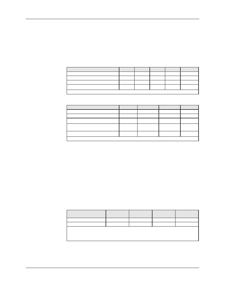
CX82100 Home Network Processor Data Sheet
2-18
Conexant Proprietary and Confidential Information
101306C
2.2.2
Operating Conditions, Absolute Maximum Ratings, and Power Consumption
CX82100 HNP operating conditions are specified in Table 2-6.
CX82100 HNP absolute maximum ratings are stated in Table 2-7.
CX82100 HNP power consumption is listed in Table 2-8.
Table 2-6. CX82100 HNP Operating Conditions
Parameter
Symbol
Min
Typ
Max
Units
Core circuits supply voltage
VDD
1.65
1.8
1.95
VDC
I/O circuits supply voltage
VDDO
3.0
3.3
3.6
VDC
I/O clamp voltage
VGG*
VDC
Operating ambient temperature
T
A
0
70
∞C
*Connect VGG to the highest signaling level being used to drive input signals, i.e. +3.3 V or +5 V.
Table 2-7. CX82100 HNP Absolute Maximum Ratings
Parameter
Symbol
Min
Max
Units
Core circuits supply voltage
VDD
-0.35
2.0
VDC
I/O circuits supply voltage
VDDO
-0.35
3.7
VDC
Input voltage
V
IN
-0.35
VGG + 0.35*
VDC
Voltage applied to outputs in high
impedance (Off) state
V
HZ
-0.35
VGG + 0.35*
VDC
Storage temperature
T
S
-55
125
∞C
* VGG = +3.3 V ± 0.3 V or +5 V ± 0.25 V.
Caution: Handling CMOS Devices
These devices contain circuitry to protect the inputs against damage due to high static
voltages. However, normal precautions should be taken to avoid application of any
voltage higher than maximum rated voltage.
An unterminated input can acquire unpredictable voltages through coupling with stray
capacitance and internal crosstalk. Both power dissipation and device noise immunity
degrades. Therefore, all inputs should be connected to an appropriate supply voltage.
Input signals should never exceed the voltage range from 0.5V or more negative than
GND to 0.5V or more positive than VDD. This prevents forward biasing the input
protection diodes and possibly entering a latch up mode due to high current transients.
Table 2-8. CX82100 HNP Power Consumption
Supply Voltage
Typical
Current (mA)
Maximum
Current (mA)
Typical
Power (mW)
Maximum
Power (mW)
VDD
85
105
155
205
VDDO
15
25
45
90
Test conditions:
VDD = +1.8 VDC for typical values;
VDD = +1.95 VDC for maximum values.
VDDO = +3.3 VDC for typical values;
VDDO = +3.6 VDC for maximum values.

CX82100 Home Network Processor Data Sheet
101306C
Conexant Proprietary and Confidential Information
2-19
2.3
Optional GPIO and Host Signal Usage
Optional GPIO and host signal usage is listed in Table 2-9.
Recommended GPIO signals are described in Table 2-10.
Table 2-9. CX82100 HNP Recommended GPIO and Host Signal Use
Pin Name
Pin
Default Use
Recommended Use
Signal Label
Reset
State
Notes
FCLKIO/GPIO39
J1
GPIO39
Z(pu)
BCLKIO/GPIO38
J5
GPIO38
Z(pu)
HAD31 (HCS4#)/GPIO37
J8
HAD31 (HCS4#)
HCS4#:
High
5
HC00 (HCS0#)/GPIO32
P14
HC00 (HCS0#)
HCS0#: Flash ROM CE#
High
2, 5
GPIO31
C6
--
Z(pu)
3
GPIO27
G4
--
Z(pu)
3
GPIO26
A8
--
Z(pu)
3
GPIO25
M7
--
Z(pu)
3
GPIO24
A1
--
Z(pu)
3
USB_PWR_DET (GPIO22)
C9
--
USB Power Detect
USB_PWR_DET
Z
2, 6
GPIO21
C3
--
Z(pu)
3
GPIO20
B1
--
LAN 1 Reset
LAN1_RST#
Z(pu)
3
GPIO19
B2
--
Z(pu)
3
GPIO18
A2
--
Z(pu)
3
GPIO17
A3
--
Low
3, 5
I2C_CLOCK (GPIO16)
E3
--
Serial EEPROM Shift Clock
I2C_CLOCK
Z(pu)
2
I2C_DATA (GPIO15)
E2
--
Serial EEPROM Data
I2C_DATA
Z(pu)
2
BOPT (GPIO14)
K4
--
Boot Loader Option
BOPT
Z(pu)
2
GPIO8
D5
--
Low
3, 5
GPIO7
E5
--
Ready Indicator
LED_READY
Z(pu)
3
GPIO6
D6
--
LAN 2 Reset
LAN2_RST#
Z(pu)
3
GPIO5
E6
--
Z(pu)
3
Notes:
1. Refer to applicable reference design information for exact GPIO use.
2. Recommended system use. See Table 2-2 for signal definition.
3. Recommended application use. See Table 2-4 for signal definition.
4. The Reset State column indicates the state of the pin upon power-on and whether or not it has an internal pullup. Z means a
high impedance state (an input) and pu/pd means the pin has an internal pullup/pulldown.
5. GPIOs that default to chip selects (GPIO32 and GPIO37), as well as GPIO8 and GPIO17, default to output upon power-on.
6. GPIO22 is the only GPIO that does not have an internal pullup/down, so if USB detect is important or used, GPIO22 should
be assigned to it. If GPIO22 is not used, or the firmware does not configure it to an output upon initialization, an external
pullup/down must be implemented on the board.
CX82100 Home Network Processor Data Sheet
2-20
Conexant Proprietary and Confidential Information
101306C
Table 2-10. CX82100 HNP Definitions of Recommended GPIO and Host Signals
Pin Signal
Pin No.
I/O
I/O Type
Signal Name/Description
LED Indicator Interface
LED_READY (GPIO7)
E5
O
Itpu/Ot4
READY Indicator. Active high output indicating the HNP is ready.
Connect LED_READY (GPIO7) to the LED plus terminal. Connect
the LED minus terminal to +3.3V through 100
.
LAN 1 Interface
LAN1_RST# (GPIO20)
B1
O
Itpu/Ot4
LAN 1 Reset. Active low reset asserted to reset the LAN 1 EPHY.
Connect to LAN 1 EPHY RSTB pin through 1 K
. Also, connect the
LAN 1 EPHY RSTB pin to +3.3V through 10 K
and to GND
through 0.1
µF.
LAN 2 Interface
LAN2_RST# (GPIO6)
D6
O
Itpu/Ot4
LAN 2 Reset. Active low output asserted to reset the LAN 2 EPHY.
Connect to LAN 2 EPHY RSTB pin through 1 K
. Also, connect the
LAN 2 EPHY RSTB pin to +3.3V through 10 K
and to GND
through 0.1
µF.
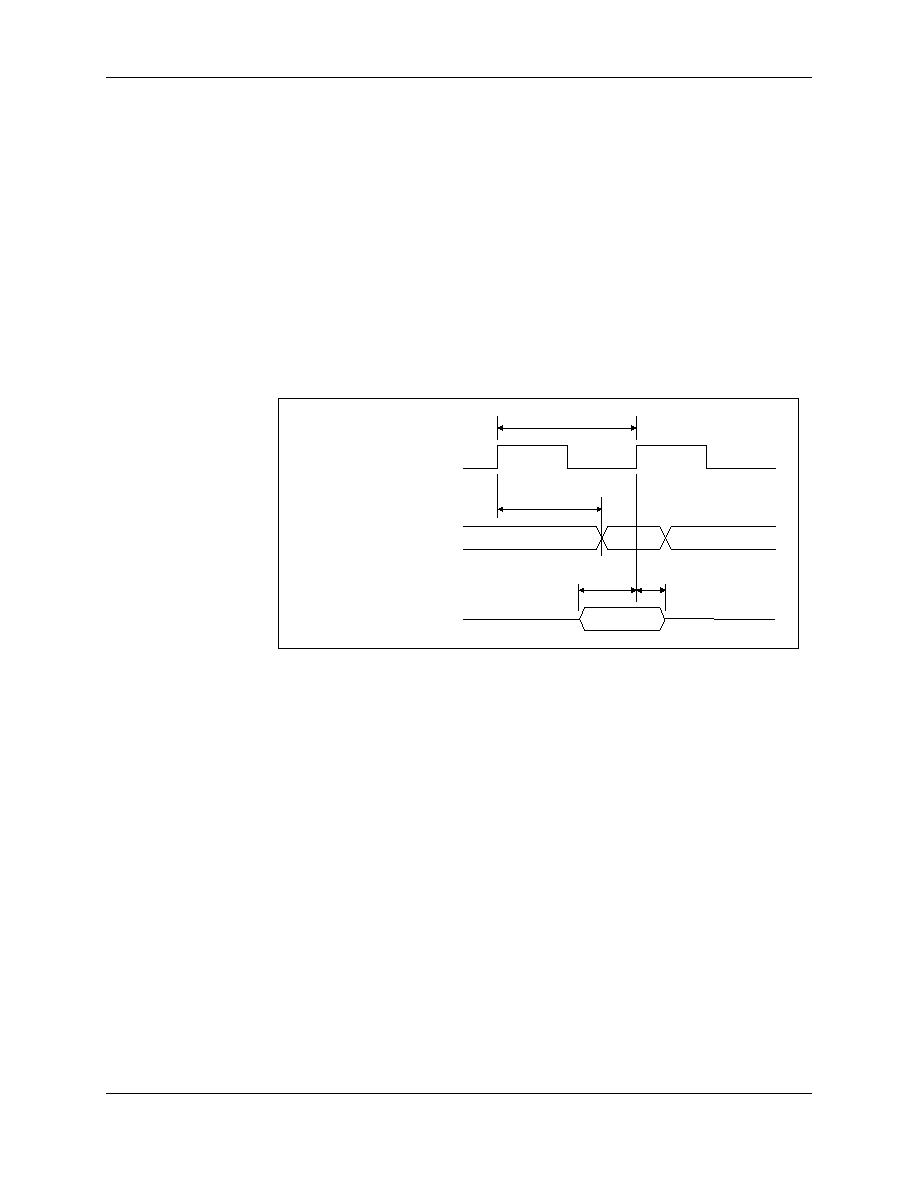
CX82100 Home Network Processor Data Sheet
101306C
Conexant Proprietary and Confidential Information
2-21
2.4
Interface Timing and Waveforms
2.4.1
External Memory Interface (SDRAM)
The External Memory Interface provides a PC100-compatible SDRAM interface. Signal
interface timing is summarized in Figure 2-5.
Note that MCLK is derived from the BCLK PLL output (see Section 12). Accordingly,
there is no fixed relationship between the HNP clock input (CLKI pin) and the External
Memory Interface signals.
Figure 2-5. External Memory Interface Timing
10 ns m in.
1 ns m in.
7.5 ns m ax.
4 ns min.
1 ns m in.
MCLK
MCKE, MA[11:0] MB[1:0], MM[1:0],
MCAS#, MRAS#, MW E#
MD[15:0] (to SDRAM)
MD[15:0] (from SDRAM)
101545_072
2.4.2
Host Interface Timing
The signal interface timing for the Host Interface is user programmable. By programming
the registers associated with the Host interface, desired timing characteristics such as
read/write pulse widths and setup and hold times can be established. For details regarding
Host Interface timing, refer to Section 5.1.5.
2.4.3
EMAC Interface Timing
To be added.
2.4.4
USB Interface Timing
To be added.
2.4.5
GPIO Interface Timing
The GPIO outputs are derived from the BCLK PLL output (see clocking chapter).
Accordingly, there is no fixed relationship between the HNP's clock input (CLKI) and
the GPIO signals.

CX82100 Home Network Processor Data Sheet
2-22
Conexant Proprietary and Confidential Information
101306C
2.4.6
Interrupt Timing
To be added.
2.4.7
Clock Reset Timing
To be added.
2.4.8
Reset Timing
To be added.
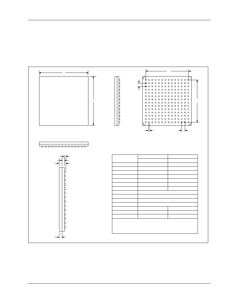
CX82100 Home Network Processor Data Sheet
101306C
Conexant Proprietary and Confidential Information
2-23
2.5
Package Dimensions
The package dimensions for the 196-pin 15 mm x 15 mm FPBGA are shown in Figure
2-6.
Figure 2-6. Package Dimensions ≠ 196-Pin 15 mm x 15 mm FPBGA
D1
E1
14 13 12 11 10 9 8 7
6 5 4 3 2 1
A
B
C
D
E
F
G
H
J
K
M
N
P
L
e
e
b
Bottom View
Top View
Side View
A1
c
A
A2
D
E
PD_GP00-D608-001
A
A1
A2
D
D1
E
E1
M
N
e
b
c
Coplanarity
W arpage
Min.
0.31
0.65
0.29
Max.
1.50
0.41
0.75
0.39
0.12
0.10
15.00 REF
13.00 REF
15.00 REF
13.00 REF
1.00 REF
0.46 REF
14
Min.
0.012
0.026
0.011
0.591 REF
0.512 REF
0.591 REF
0.521 REF
0.031 REF
0.018 REF
Max.
0.059
0.016
0.030
0.015
0.005
0.004
196
Millimeters
Inches*
Dimension
Ref: GP00-D608-001
* Dimensions in inches are for reference only;
use metric dimensions for board design.

CX82100 Home Network Processor Data Sheet
2-24
Conexant Proprietary and Confidential Information
101306C
This page is intentionally blank.

CX82100 Home Network Processor Data Sheet
101306C
Conexant Proprietary and Confidential Information
3-1
3
HNP Memory Architecture
3.1
HNP Memory Map
The HNP system memory map is shown in Figure 3-1. All internal and external memory
and APB peripheral registers are memory-mapped directly to the first 16 MB region of
the ASB 32-bit address space. Note that the map shows only the memory range reserved
for each ASB slave. The actual memory size required by each slave varies depending on
its design. Each memory area is allocated with a fixed starting address (i.e., it is not
relocatable).
From the figure, it can be seen that there are two different memory maps, Run-time and
Boot-time. The reason for the different maps is to allow the Operating System (OS) to
change the ARM exception vectors located at address 0x0 at run-time. Once boot is
complete and memory maps are switched (external Flash ROM and internal RAM
address space is swapped), the OS may change these exception vectors since they are
now located in RAM.
CX82100 Home Network Processor Data Sheet
3-2
Conexant Proprietary and Confidential Information
101306C
Figure 3-1. HNP Memory Map
101545_007
Run-Time
Memory Map
0x00000000
0x00180000
0x001FFFFF
0x00200000
0x002FFFFF
0x00300000
0x000FFFFF
0x00100000
0x0017FFFF
0x003FFFFF
0x00400000
0x007FFFFF
0x00800000
0x00FFFFFF
0x01000000
Reserved
(512 kB)
0x0007FFFF
0x00080000
16 MB Space
0xFFFFFFFF
0x80000000
Reserved
(512 kB)
Reserved for Internal RAM
Expansion (480 kB)
Internal RAM (32 kB)
ARM Vector Table (32 Bytes)
Host Master Mode
Interface
(1 MB)
ASB-to-APB Bridge/DMAC
and
APB Peripherals
(1 MB)
External Flash
(4 MB)
External SDRAM/SRAM
(8 MB)
Reserved
(4 GB - 16 MB)
Reserved
(4 GB - 16 MB)
(Continued)
Reserved for Internal ROM
Expansion (448 kB)
Internal ROM (64 kB)
ARM Vector Table (32 Bytes)
Internal Boot ROM/
External Flash ROM
(1 MB)
Internal RAM
(512 kB)
Reserved
(512 kB)
Host Master Mode
Interface
(1 MB)
ASB-to-APB Bridge/DMAC
and
APB Peripherals
(1 MB)
External Flash
(4 MB)
External SDRAM/SRAM
(8 MB)
Reserved
(4 GB - 16 MB)
Reserved
(4 GB - 16 MB)
(Continued)
Boot-Time
Memory Map
TIC Access
CX82100 Home Network Processor Data Sheet
101306C
Conexant Proprietary and Confidential Information
3-3
3.2
Starting Addresses
The starting addresses for mapping ASB and APB slaves are defined in Table 3-1 and
Table 3-2, respectively.
Table 3-1. Starting Addresses for Mapping ASB Slaves
ASB Address:
BA[31:0]
ASB Slave
Description
0x000XXXXX
External Flash
ROM/Internal RAM
16k x 32 Internal ROM/External Flash ROM
(Boot-Time);
8k x 32 Internal RAM (Run-Time)
0x0018XXXX
Internal RAM/Internal ROM
8k x 32 Internal RAM (Boot-Time);
16k x 32 Internal ROM (Run-Time)
0x002XXXXX
Host Interface
Host Master Mode peripherals interface
0x003XXXXX
ASB-to-APB Bridge/DMAC
To ASB-to-APB Bridge and APB peripherals
≠ dword (4 bytes) access only
0x00400000≠
0x007FFFFF
External Flash ROM
Host Master Mode interface to 4 MB Flash
0x00800000 -
0x00FFFFFF
External SDRAM
External SDRAM/SRAM interface to 8 MB
SDRAM or up to 1 MB SRAM
0x80000000
ARM940T
ARM940T TIC Access
Table 3-2. Starting Addresses for Mapping APB Slaves
ASB Address:
BA[31:0]
APB Slave
Description
0x0030XXXX
ASB-to-APB Bridge/DMAC
ASB-to-APB Bridge Slave and DMAC
0x0031XXXX
EMAC 1
Ethernet Media Access Control 1
0x0032XXXX
EMAC 2
Ethernet Media Access Control 2
0x0033XXXX
USB Interface
USB Device Controller
0x0034XXXX
Reserved
0x0035XXXX
Interrupts, Timers, GPIO,
Clock (ITGC)
Miscellaneous Peripherals (Interrupts, Timers,
GPIOs, and Clock)
3.2.1
ARM Vector Table
Table 3-3 shows the exception vector addresses required by the ARM940T. The first 32-
byte space of the ASB address space is reserved for this table.
Table 3-3. ARM Exception Vector Addresses
Address
Exception
Mode on Entry
0x00000000
Reset
Supervisor
0x00000004
Undefined Instruction
Undefined
0x00000008
Software Interrupt
Supervisor
0x0000000C
Abort (Prefetch)
Abort
0x00000010
Abort (Data)
Abort
0x00000014
Reserved
Reserved
0x00000018
IRQ#
IRQ#
0x0000001C
FIQ#
FIQ#
CX82100 Home Network Processor Data Sheet
3-4
Conexant Proprietary and Confidential Information
101306C
3.3
Endianness
The internal bus architecture supports only Little-Endian mode addressing (see Figure
3-2). Support for Big-Endian mode may occur in a peripheral that handles its data stream
or in the host interface which may exchange data with a Big-Endian mode external
processor.
Figure 3-2. Little-Endian Mode Addressing
100878-008
31:24
7:0
15:8
23:16
Data Bus
Byte Lane No.
0
2
3
1
BA[1:0]=3
BA[1:0]=0
BA[1:0]=1
BA[1:0]=2
3.4
Boot Procedure
There are two different scenarios for the boot procedure depending on the state of the
BOPT (GPIO14) pin. Upon power-on or reset, boot code will execute from internal ROM
if the BOPT (GPIO14) pin is high or from external Flash ROM if the BOPT (GPIO14)
pin is low.
When booting from internal ROM, the boot code reads EEPROM information (if an
EEPROM is installed) to set up the USB configuration of the HNP. Once complete, USB
communication between PC and the HNP can occur.
When booting from external Flash ROM, the HNP maps the first MB of external Flash
ROM space to internal ROM space (see memory map in Figure 3-1 for detailed
information). A typical boot procedure begins by copying the flash boot code to internal
RAM. The RUN_MAP bit is set in the Host Control Register (see 5.3.1) which causes the
boot code to begin execution from internal RAM. The boot code then configures the
clocks and the enables the SDRAM. This enables the boot code to begin execution from
internal RAM. The boot code then copies the application firmware residing in flash to
SDRAM. The boot code then jumps to the start of the application firmware in SDRAM.
Figure 3-3 illustrates the boot procedure.
CX82100 Home Network Processor Data Sheet
101306C
Conexant Proprietary and Confidential Information
3-5
Figure 3-3. Boot Procedure
Power-On-Reset
Begin execution of the
ROM code.
Read signature
bytes (first 4
bytes) of
EEPROM.
Is the signature
present?
Read from EEPROM,
Device Descriptor, Device
Config., endpoint config.,
Lang. string ID, Manuf.
string ID, Prod. string ID,
and store in SRAM.
Load UDC, EPINFO,
ENDPTBUFs,
CONFIGBUFs,
STRINGBUFs, with
SRAM data.
Continuous loop
waiting for USB
traffic.
Read from internal ROM,
Device Descriptor, Device
Config., endpoint config.,
Lang. string ID, Manuf.
string ID, Prod. string ID,
and store in SRAM.
Y
N
Power-On-Reset
Begin execution of Flash
m apped to ROM address
space.
Flash boot code
copies itself into
SRAM.
Set Run-Map bit to
swap ROM and RAM
address space. Now
executing out of
SRAM.
Enable SDRAM.
Set up
FCLK and BLCK
frequencies.
Copy application
firm ware from
flash to SDRAM.
Jum p to start of
application firm ware
in SDRAM and
execute.
GPIO14 boot option pin
Flash boot(GPIO14=0)
Internal ROM boot(GPIO14=1)
Typical Flash
boot scenario.
101545_009

CX82100 Home Network Processor Data Sheet
3-6
Conexant Proprietary and Confidential Information
101306C
This page is intentionally blank.

CX82100 Home Network Processor Data Sheet
101306C
Conexant Proprietary and Confidential Information
4-1
4
DMAC Interface Description
The DMA controller (DMAC) is both an ASB master and an APB master. It is integrated
with the ASB-to-APB bridge. Using burst transfers and pipelining the data within the bus
bridge interface optimizes ASB efficiency.
The DMAC always performs qword (8 bytes) data transfers which require data valid on
the entire 64-bit APB data bus. Burst transfer on APB is not supported, however, data can
be transferred on consecutive APB cycles (PCLK cycles) for either read or write.
4.1
DMA Channel Definition
The DMAC supports the data stream channels defined in Table 4-1. Each channel's data-
flow is considered with respect to the system memory's point-of-view. A source channel
has the memory supplying data to the DMAC and on to the transmitter's output port. A
destination channel is one where the memory receives data through the DMAC from the
receiver's input port.
Table 4-1. DMA Channel Definition for DMAC
DMA Channel No.
Channel Type
Channel Description
DMA Mode
1
Src/Dst
EMAC1-TxD
Lnk Lst ≠ restart
2
Dst
EMAC1-RxD
Circ Bfr ≠ restart
3
Src/Dst
EMAC2-TxD
Lnk Lst ≠ restart
4
Dst
EMAC2-RxD
Circ Bfr ≠ restart
5
Src
Reserved
6
Dst
Reserved
7
Src
M2M In
Src
8
Dst
M2M Out
Dst
9
Src
USB-TxD_EP3
Lnk Lst
10
Src
USB-TxD_EP2
Lnk Lst
11
Src
USB-TxD_EP1
Lnk Lst
12
Dst
USB-RxD
Circ Bfr ≠ restart
13
Src
USB-TxD_EP0
Lnk Lst
4.2
DMA Requests and Data Transfer
The APB peripherals issue DMA data transfer requests to the DMAC. The knowledge of
how much data will be received or transmitted resides within the peripheral. The physical
interface transfers can be controlled to bit transfer resolution even though the DMAC
only operates at qword resolution. So the size of the packets actually DMAed (which may
differ from that transmitted or received) is under peripheral control. The DMAC just
generates sequential incrementing addresses. Table 4-2 lists all the request commands
supported by DMAC.
DMA action requests are signaled by encoding X{x}R where {x} represents the channel
number. The signal X{x}R should remain idle except when issuing a specific request to
the DMAC. Each event is signaled during a single PCLK clock cycle. It is acceptable to
have an interrupt or abort event directly follow a data transfer request. When an APB data
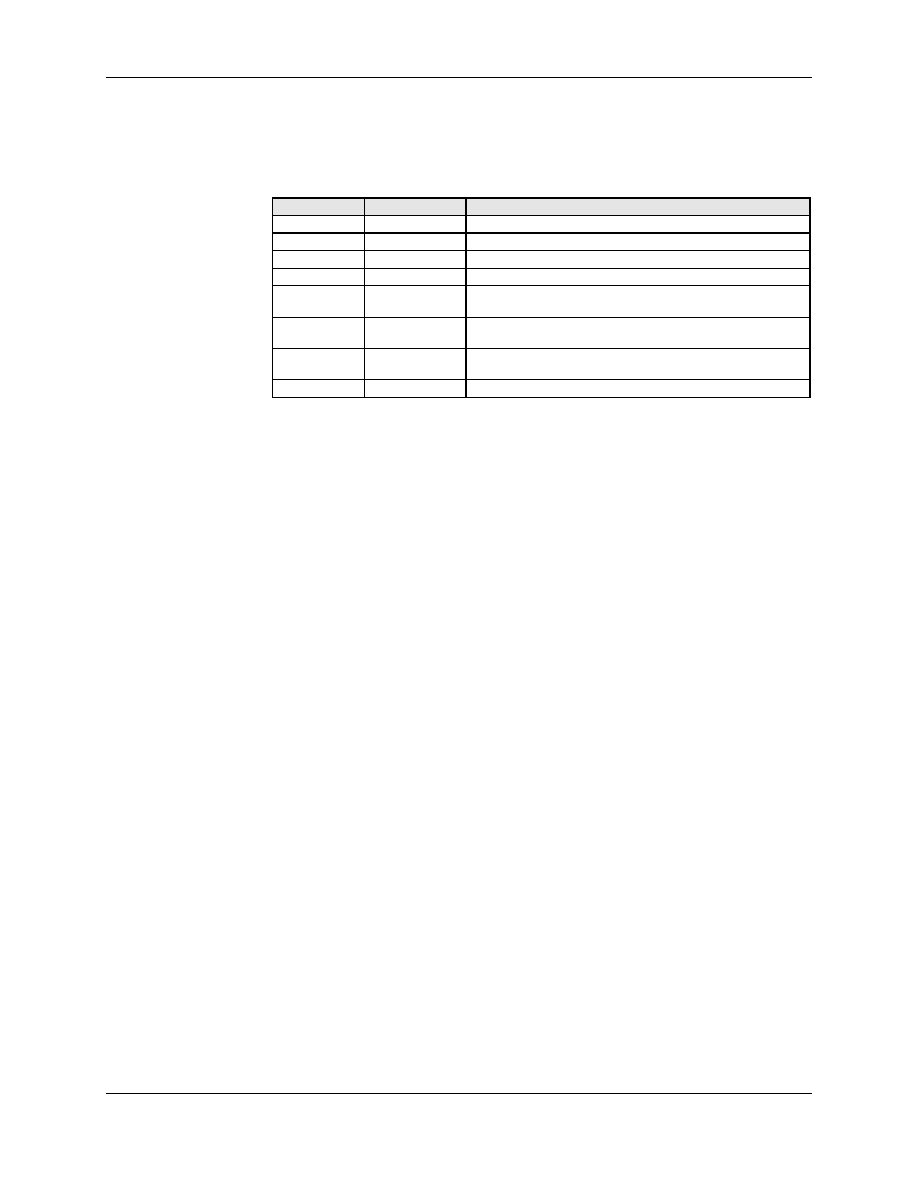
CX82100 Home Network Processor Data Sheet
4-2
Conexant Proprietary and Confidential Information
101306C
peripheral makes a DMA data transfer request, however, it should not make another until
after the current request has been processed (APB read or write). It is left up to the
requestor (not the DMAC) to log any overflow or underflow conditions.
Table 4-2. DMA Requests for APB Peripherals
X{x}R
Request
DMAC Action
3'b000
DMA_IDLE
None
3'b001
DMA_INTR
Data Pkt Done interrupt forwarded to interrupt controller.
3'b010
DMA_SAVE
Save channel's state (cnt and/or ptr).
3'b011
DMA_RELD
Reload or restore channel's state from previous save.
3'b100
DMA_XNXT
Data transfer request @ current pointer. Ptr1+ = 8 (1 qword),
Cnt1-- (Cnt1 represents the number of qwords)
3'b101
DMA_XSAV
Data transfer request @ saved pointer. Ptr2+ = 8 (1 qword),
Cnt2-- (Cnt2 represents the number of qwords)
3'b110
DMA_XNUL
Advance current pointer, skip data transfer. Ptr1+ = 8
(1 qword), Cnt1-- (Cnt1 represents the number of qwords)
3'b111
Reserved
Note that DMA_XNXT and DMA_XSAV are the only DMA commands that cause a
data transfer. Once issued, the channel requestor should not issue another until after their
APB DMA port has been accessed. The APB DMA port qword read or write serves as
the DMAC acknowledge to the channel requestor.
The actions DMA_SAVE, DMA_RELD, and DMA_XNUL should not be issued during
a pending data transfer request since the current pointer and counter are not updated until
the channel is serviced. Usually DMA_SAVE will be issued just after the packet's last
qword transfer acknowledge. Usually DMA_RELD is issued when a channel decides to
abort a packet. DMA_XNUL is typically issued before starting a packet transfer.
The action DMA_XNUL can be issued on consecutive PCLKs if the channel desires to
move up its current pointer by several qwords. This action may not be issued when the
DMAC_{x}_Cnt1 is equal to 1. DMA_XNUL may not be used just before an address
link. Normally, when DMA_XNXT is issued for the last data qword, both the link and
data transfers are scheduled concurrently, with the link transfer actually occurring first.
Two problems arise if DMA_XNUL is allowed to decrement the qword counter quickly.
First, the address is changed before a link transfer can be scheduled into the DMAC
transfer queue with the correct address. Second, there is nothing to prevent the requesting
channel from issuing a DMA_XNXT before the new address link is updated.
4.3
Control Registers
Per each DMA channel {x}, the DMAC can support three basic modes of address
generation using up to two 22-bit dword- (4 bytes) aligned address pointers
(DMAC_{x}_Ptr1, DMAC_{x}_Ptr2) and/or up to three 11-bit qword (8 bytes) counters
(DMAC_{x}_Cnt1, DMAC_{x}_Cnt2, DMAC_{x}_Cnt3). DMAC_{x}_Ptr1 will
always be readable as the current qword pointer. The counters are large enough to allow a
maximum DMA contiguous block transfer of 16 KB (less 1 qword). Each channel {x} is
handled uniquely and specifically for operating mode, priority, and data rate. Recall that
the peripheral is in control of initiating, aborting, and ending the DMA transfer requests.
Pointers are 22-bit programmable and dword-aligned. The pointer registers are bit-
aligned to represent the pointers as 24-bit byte-addresses. Thus the pointer registers
should be written and read as 24-bit byte-addresses. However, the lower two bits are
fixed at 2'b00 forcing the pointers to be dword-aligned. Recall that data transfer
resolution is limited to whole qwords.

CX82100 Home Network Processor Data Sheet
101306C
Conexant Proprietary and Confidential Information
4-3
4.4
DMAC Register Memory Map
DMAC registers are identified in Table 4-3.
Table 4-3. DMAC Registers
Register Label
Register Name
ASB Address
Type
Default Value
Ref.
DMAC_1_Ptr1
DMAC 1 Current Pointer 1
0x00300000
RW*
0x00000000
4.5.1
DMAC_2_Ptr1
DMAC 2 Current Pointer 1
0x00300004
RO
0x00000000
4.5.1
DMAC_3_Ptr1
DMAC 3 Current Pointer 1
0x00300008
RW*
0x00000000
4.5.1
DMAC_4_Ptr1
DMAC 4 Current Pointer 1
0x0030000C
RO
0x00000000
4.5.1
DMAC_5_Ptr1
DMAC 5 Current Pointer 1
0x00300010
RW*
0x00000000
4.5.1
DMAC_6_Ptr1
DMAC 6 Current Pointer 1
0x00300014
RW*
0x00000000
4.5.1
DMAC_7_Ptr1
DMAC 7 Current Pointer 1
0x00300018
RW*
0x00000000
4.5.1
DMAC_8_Ptr1
DMAC 8 Current Pointer 1
0x0030001C
RW*
0x00000000
4.5.1
DMAC_9_Ptr1
DMAC 9 Current Pointer 1
0x00300020
RW*
0x00000000
4.5.1
DMAC_10_Ptr1
DMAC 10 Current Pointer 1
0x00300024
RW*
0x00000000
4.5.1
DMAC_11_Ptr1
DMAC 11 Current Pointer 1
0x00300028
RW*
0x00000000
4.5.1
*** Reserved ***
0x0030002C
DMAC_1_Ptr2
DMAC 1 Indirect/Return Pointer 2
0x00300030
RW*
0x00000000
4.5.4
DMAC_2_Ptr2
DMAC 2 Indirect/Return Pointer 2
0x00300034
RW*
0x00000000
4.5.4
DMAC_3_Ptr2
DMAC 3 Indirect/Return Pointer 2
0x00300038
RW*
0x00000000
4.5.4
DMAC_4_Ptr2
DMAC 4 Indirect/Return Pointer 2
0x0030003C
RW*
0x00000000
4.5.4
DMAC_5_Ptr2
DMAC 5 Indirect/Return Pointer 2
0x00300040
RW*
0x00000000
4.5.4
*** Reserved ***
0x00300044≠
0x0030005C
DMAC_1_Cnt1
DMAC 1 Buffer Size Counter 1
0x00300060
RW*
0x00000000
4.5.3
DMAC_2_Cnt1
DMAC 2 Buffer Size Counter 1
0x00300064
RW*
0x00000000
4.5.3
DMAC_3_Cnt1
DMAC 3 Buffer Size Counter 1
0x00300068
RW*
0x00000000
4.5.3
DMAC_4_Cnt1
DMAC 4 Buffer Size Counter 1
0x0030006C
RW*
0x00000000
4.5.3
DMAC_5_Cnt1
DMAC 5 Buffer Size Counter 1
0x00300070
RW*
0x00000000
4.5.3
DMAC_6_Cnt1
DMAC 6 Buffer Size Counter 1
0x00300074
RW*
0x00000000
4.5.3
*** Reserved ***
0x00300078≠
0x0030007C
DMAC_9_Cnt1
DMAC 9 Buffer Size Counter 1
0x00300080
RW*
0x00000000
4.5.3
DMAC_10_Cnt1
DMAC 10 Buffer Size Counter 1
0x00300084
RW*
0x00000000
4.5.3
DMAC_11_Cnt1
DMAC 11 Buffer Size Counter 1
0x00300088
RW*
0x00000000
4.5.3
*** Reserved ***
0x0030008C≠
0x00300090
DMAC_2_Cnt2
DMAC 2 Buffer Size Counter 2
0x00300094
WO
0x00000000
4.5.4
*** Reserved ***
0x00300098
DMAC_4_Cnt2
DMAC 4 Buffer Size Counter 2
0x0030009C
WO
0x00000000
4.5.4
*** Reserved ***
0x003000A0≠
0x003000FC
DMAC_12_Ptr1
DMAC 11 Current Pointer 1
0x00300100
RW*
0x00000000
4.5.1
DMAC_13_Ptr1
DMAC 12 Current Pointer 1
0x00300104
RW*
0x00000000
4.5.1
*** Reserved ***
0x00300108≠
0x0030010C
DMAC_12_Cnt1
DMAC 11 Buffer Size Counter 1
0x00300110
RW*
0x00000000
4.5.3
DMAC_13_Cnt1
DMAC 12 Buffer Size Counter 1
0x00300114
RW*
0x00000000
4.5.3
*** Reserved ***
0x00300118≠
0x00300124

CX82100 Home Network Processor Data Sheet
4-4
Conexant Proprietary and Confidential Information
101306C
4.5
Control Register Formats
4.5.1
DMAC x Current Pointer 1 (DMAC_{x}_Ptr1)
Bit(s)
Type
Default
Name
Description
31:24
Reserved.
23:2
RW*
22'bx
DMAC_{x}_Ptr1
Current DMA qword Address Pointer.
Points to next qword transfer location within source or destination
buffer. Always dword-aligned.
1:0
Reserved.
4.5.2
DMAC x Indirect/Return Pointer 1 (DMAC_{x}_Ptr2)
Bit(s)
Type
Default
Name
Description
31:24
Reserved.
23:2
RW*
22'bx
DMAC_{x}_Ptr2
Indirect or Return DMA qword Address Pointer.
Points to next pointer which points to next qword transfer location
within source or destination buffer. Always dword-aligned.
1:0
Reserved.
4.5.3
DMAC x Buffer Size Counter 1 (DMAC_{x}_Cnt1)
Bit(s)
Type
Default
Name
Description
31:26
Reserved.
25:24
RW
2'b00
DMAC_{x}_LMode
DMA Linked List Mode.
00 =
ptr/cnt at buffer tail.
01 =
ptr/cnt at Ptr2 (table).
10 =
ptr/cnt at Ptr2 (return ptr).
11 =
Reserved.
23:11
Reserved.
10:0
RW*
11'bx
DMAC_{x}_Cnt1
Initialize to DMA Buffer Size in No. of qwords.
Decrements during DMA data transfers and reloads at end of buffer.
Note that a write to DMAC_{x}_Cnt1 also loads buffer size to
DMAC_{x}_Cnt2.
4.5.4
DMAC x Buffer Size Counter 2 (DMAC_{x}_Cnt2)
Bit(s)
Type
Default
Name
Description
31:11
Reserved.
10:0
RW*
11'bx
DMAC_{x}_Cnt2
Saved DMA Buffer Size in No. of qwords.

CX82100 Home Network Processor Data Sheet
101306C
Conexant Proprietary and Confidential Information
4-5
4.5.5
DMAC x Buffer Size Counter 3 (DMAC_{x}_Cnt3)
Bit(s)
Type
Default
Name
Description
31:11
Reserved.
10:0
RW*
11'bx
DMAC_{x}_Cnt3
Saved DMA Buffer Size in No. of qwords.
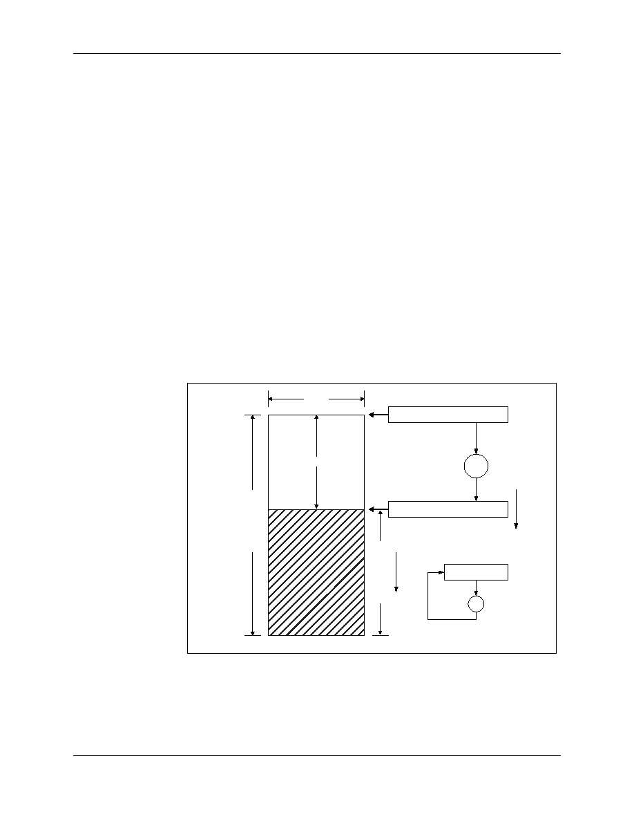
CX82100 Home Network Processor Data Sheet
4-6
Conexant Proprietary and Confidential Information
101306C
4.6
Three Basic Modes of Address Generation
4.6.1
Source or Destination Mode
DMAC_{x}_Ptr1 is initialized by the microcontroller to point to the beginning of a
dword-aligned source or destination buffer. This pointer advances (by 1 qword) after
each transfer request X{x}R. Reading this pointer returns the current qword location to
be handled next by the DMAC when it processes the channel request.
4.6.2
Circular Buffer Modes
Two circular buffer modes are supported:
∑ The direct circular buffer for the downstream USB receive data channels.
∑ The indirect circular pointer table for the Ethernet receive channels.
Direct Circular Buffer
Figure 4-1 depicts how the addresses are generated in the Direct Circular Buffer mode.
Figure 4-1. Address Generation in Direct Circular Buffer Mode
101545_010
D
M
A
C
_{
x
}
_
C
nt
2
D
M
A
C
_{
x
}
_C
nt
1
Base Pointer
DMAC_{x}_Ptr2
=
DMAC_{x}_C nt2 -
DMAC_{x}_C nt1
Top
Bottom
+
8*
Current Pointer DMAC_{x}_Ptr1
D MAC_{x}_Cnt1
-1
(Fixed)
(Fixed)
(
M
o
v
i
ng)
(M
o
v
i
n
g
)
8 Bytes
CX82100 Home Network Processor Data Sheet
101306C
Conexant Proprietary and Confidential Information
4-7
The usage of each register for controlling the operation of the circular buffer is as
follows:
∑ DMAC_{x}_Ptr2. Used as a base pointer to a dword-aligned circular buffer and is
loaded by the microcontroller (by writing to DMAC_{x}_Ptr1) just once (i.e., this
pointer value is fixed) after the buffer has been allocated. This buffer is typically big
enough to handle multiple data packets (packet size is 64 bytes for USB). The buffer
must be a whole multiple of qwords.
∑ DMAC_{x}_Ptr1. Used as the current pointer, pointing to the next qword to be
transferred. This pointer is constructed by adding 8*(DMAC_{x}_Cnt2 ≠
DMAC_{x}_Cnt1) to the base pointer DMA{x}_Ptr2. The constructed
DMAC_{x}_Ptr1 is the value read when reading its register location (writing has no
effect for the Circular Buffer mode).
∑ DMAC_{x}_Cnt1. Loaded with an 11-bit value representing the size of the entire
circular buffer. The same value is copied to DMAC_{x}_Cnt2 during write to
DMAC_{x}_Cnt1. This counter register is decremented by one as a qword transfer
is processed. When DMA{x}_Cnt1 = 0, it is reloaded with DMAC_{x}_Cnt2.
∑ DMAC_{x}_Cnt2. Loaded with an 11-bit value representing the size of the entire
circular buffer. This value is not changed during the course of data transfers.
Indirect Circular Pointer Table
The indirect circular pointer table is explained with an example of how the EMAC RxD
channels work. The EMAC-RxD channel (channel 2 or 4) requires its data to be stored in
memory buffers where the location of each buffer is chosen by the firmware on a pointer
per packet basis. Each received data packet is stored in a contiguous memory segment of
fixed size. This size must be large enough to handle the largest expected packet (plus
overhead), usually less than 1536 bytes (192 qwords). The data is normally going to
remain stationary until transmitted or consumed. The circular data buffer method is not
appropriate for this channel because it would require the data to be consumed in the order
received otherwise the data would have to be copied to other buffers which consumes a
lot of bus bandwidth.
The DMA_{x}_Ptr2, where {x} = 2 or 4, is used to point to the location of the table
which contains the list of pointers to be used for the received data destination buffers.
This table holds the following 4-dword structures called cluster descriptors:
Table 4-4. Cluster Descriptor Table
Cluster Descriptor Table (CDT)
DMA_{x}_Ptr2, where {x} = 2 or 4
CD No.
qword
dword
Cluster Pointer 1
1
Reserved
EMAC-RxD Status [31:0] for packet 1
1
2
EMAC-RxD Status [63:32] for packet 1
Cluster Pointer N
2N-1
Reserved
EMAC-RxD Status [31:0] for packet N
N
2N
EMAC-RxD Status [63:32] for packet N
The cluster descriptors include status that is written back from the EMAC for each
received packet. When DMA_{x}_Ptr2 is written, a copy is saved as the base pointer to
the head of the pointer table (CDT). The DMA_{x}_Ptr2 can be read anytime to indicate
where the DMAC is currently at in the CDT. The CDT is a circular buffer. The size in

CX82100 Home Network Processor Data Sheet
4-8
Conexant Proprietary and Confidential Information
101306C
qwords is determined by DMA_{x}_Cnt2. If there are N cluster descriptors then the
value 2N should be written to DMA_{x}_Cnt2.
The DMAC prefetches the cluster pointers to a two-pointer queue using a source DMA
channel. This queue is initialized (filled) automatically as soon as the firmware writes to
DMA_{x}_Cnt2 (so CDT must be valid and DMA_{x}_Ptr2 initialized). The DMAC has
a two-pointer queue in order to reduce the latency seen by the EMAC-RxD channel when
switching from one cluster to another. The DMAC does not want to add the cluster
pointer fetch latency to the data transfer latency. The current pointer in the queue is
DMA_{x}_Ptr1 and points to the location in the cluster buffer where the received data is
to be stored. This pointer can be read anytime.
The DMA_{x}_Cnt1 value is used to limit the number of qwords the EMAC-RxD can
write to the cluster buffer. Writing a value X to this register will cause all qwords DMA
transferred past X to be stored in the same cluster location (overwritten, only last qword
visible). Reading this register will return a value that indicates the number of qwords
transferred which could be even larger than the size written to DMA_{x}_Cnt1. This
register limits how far the DMA_{x}_Ptr1 may advance. The DMA_{x}_Cnt1 value
increments by 1 for each DMA_XNXT as well as DMA_XNUL.
The EMAC-RxD DMA channel uses a state machine to control the interactions of the
firmware, EMAC-RxD DMA requests, and the DMAC. This state machine is initialized
when DMA_{x}_Cnt2 is written. This event triggers the prefetch of two cluster pointers
from the CDT. The DMA_{x}_Ptr2 will be pointing to the first EMAC-RxD status
qword location after it fills its DMA_{X}_Ptr1 queue. When the EMAC-RxD channel
issues DMA_XSAV, the packet status is read and transferred to the current
DMA_{X}_Ptr2 location. The receiver channel then issues DMA_INTR which causes
the packet interrupt. It also triggers this state machine to transfer the prefetched cluster
pointer to DMA_{X}_Ptr1 and then prefetch the next cluster pointer.
At the beginning of each packet the EMAC-RxD channel issues a DMA_SAVE to save a
copy of the DMA_{X}_Ptr1 cluster head pointer. In case of a bad packet (too short, bad
CRC, etc.) the EMAC-RxD channel will abort the packet and issue a DMA_RELD. This
event will cause the copy of the cluster head pointer to be reloaded into DMA_{X}_Ptr1
and the DMA_{X}_Cnt1 to be re-initialized to zero.
The clusters (received packets) consist of received data qwords transferred via
DMA_XNXT surrounded by reserved qwords at the head and tail of the buffers.
Table 4-5. Received Data Packet
qword No.
Cluster qword
DMA_{x}_Ptr1, {x} = 2 or 4
1
Reserved < DMA_XNUL
2
EMAC-RxD < DMA_XNXT
P-1
EMAC-RxD < DMA_XNXT
P
Reserved (0) < DMA_XNXT
...
...
X
Maximum length of packet data
X+1
Overflow location for too long packet
The 1
st
reserved qword is present because the EMAC-RxD channel issues a
DMA_XNUL at the beginning of every packet. The last reserved qword results from the
channel issuing a DMA_XNXT to transfer a zero qword. If DMA_{X}_Cnt1 is set to X,
then all qwords received after that limit for a given packet will be transferred to location
DMA_{X}_Ptr1 + 8(X+1). The DMA_XNUL does increment DMA_{X}_Cnt1. Most
packets will end much shorter than the programmed limit. In the case of a too long
received packet, the EMAC will end up aborting the packet which causes the next packet

CX82100 Home Network Processor Data Sheet
101306C
Conexant Proprietary and Confidential Information
4-9
to be stored at the same cluster location. The limiter, DMA_{X}_Cnt1, is used to prevent
the EMAC-RxD channel from overwriting the allocated cluster buffer size.
The protocol for this DMA channel is:
1. ARM initializes the CDT.
2. ARM initializes DMA_{X}_Ptr2 with the base pointer to CDT (a copy saved within
DMAC).
3. ARM initializes DMA_{X}_Cnt1 to limit number of qwords written to cluster.
4. ARM initializes DMA_{X}_Cnt2 for CDT circular size in qwords.
5. DMAC prefetches first cluster pointer from DMA_{X}_Ptr2+ = 8 (post-increments
by 8).
6. DMAC moves prefetched cluster pointer into DMA_{X}_Ptr1 and prefetches second
cluster pointer from DMA_{X}_Ptr2+8 (no post-increment).
7. EMAC-RxD issues DMA_SAVE, DMAC saves cluster head ptr.
8. EMAC-RxD issues DMA_XNUL, DMA_{X}_Ptr1+ = 8, DMA_{X}_Cnt1++.
9. EMAC-RxD issues DMA_XNXT, DMAC saves data to DMA_{X}_Ptr1+ = 8,
DMA_{X}_Cnt1++.
10. Continue with step 8 until entire packet data is received.
11. EMAC-RxD issues DMA_XSAV, DMAC saves status to DMA_{X}_Ptr2+ = 16.
12. EMAC-RxD issues DMA_XNXT, DMAC saves 0 to DMA_{X}_Ptr1+ = 8,
DMA_{X}_Cnt1++.
13. EMAC-RxD issues DMA_INTR, DMAC sets DMA interrupt for RxD channel.
14. DMAC moves prefetched cluster pointer into DMA_{X}_Ptr1 and prefetches next
cluster pointer from DMA_{X}_Ptr2+8 (no post-increment).
The ARM may read DMA_{X}_Ptr2 at anytime to know where the DMAC is currently
processing the table (recall that the DMAC is prefetching cluster pointers). The ARM can
also determine that a EMAC-RxD status qword location has been updated by looking at
bit 3 which is always written with a 1'b1, if it initializes the status qwords with zero and
as it consumes clusters (and ptrs).
Since the CDT operates in circular mode, all ptr2 prefetches and post-increments operate
modulo 8*DMA_Cnt2.
4.6.3
Linked List Mode
There are two linked list modes supported in the current design: 1) embedded tail linked
list descriptor mode and 2) indirect/table linked list descriptor mode. The first mode is
supported for all transmit channels except channel 7 (memory-to-memory DMAs). The
second mode is supported only for USB transmit channels, i.e., channels 9, 10, 11, and
13. The linked list mode can be programmed through the "DMAC_{x}_LMode" field in
the DMAC_{x}_Cnt1 registers.
Embedded Tail Linked List Descriptor Mode
For the Embedded Tail Linked List Descriptor mode, the buffer link descriptor (ptr/cnt) is
embedded in the buffer at its tail end. Figure 4-2 shows an example for this linked list
mode. This tail linked list is a generic example of how the transmitted packets are set up.
The Ctl_Hdr is specific to the type of DMA being performed, e.g., EMAC, and should be
configured accordingly.
CX82100 Home Network Processor Data Sheet
4-10
Conexant Proprietary and Confidential Information
101306C
Figure 4-2. Embedded Tail Linked List Descriptor Example
101545_010
0 x00 140 248
0 x00 140 24C
0 x00 140 250
0 x00 140 254
0 x00 140 258
0 x00 140 25C
0 x00 140 260
0 x00 140 264
0 x00 140 268
0 x00 140 26C
0 x00 140 470
0 x00 140 474
0 x00 140 478
0 x00 140 47C
0x 001 404 80
0x 001 404 84
0x 001 404 88
Next Cnt1
0x 001 404 8C
DMAC_{x}_Cnt2 = 0x004
DMAC_{x}_Ptr2= 0x00140248
3
Next Ptr1
Data
Data
Data
Data
0
1
2
Ctl Hdr
Data
0x00000003
0x00140470
4
Data
Data
Data
Data
2
3
Data
Data
1
Data
Ctl Hdr
0
DMAC_{x}_Cnt1 = 0x001
DMAC_{x}_Ptr1= 0x00140480
4 Bytes

CX82100 Home Network Processor Data Sheet
101306C
Conexant Proprietary and Confidential Information
4-11
The usage of each register for controlling the operation of the Embedded Tail Linked List
Descriptor mode is described below.
∑ DMAC_{x}_Ptr1: Loaded with an initial pointer to a dword-aligned source buffer.
A copy of the pointer is automatically saved in DMAC_{x}_Ptr2 whenever
DMAC_{x}_Ptr1 is loaded with a new pointer. As each DMA request is processed,
DMAC_{x}_Ptr1 is incremented by one qword.
∑ DMAC_{x}_Cnt1: Loaded with the number of qwords to be delivered to the
channel. This value includes the Ctl_Hdr, but not the link fields at the tail. A copy of
the counter value is automatically saved in DMAC_{x}_Cnt2 whenever
DMAC_{x}_Cnt1 is loaded with a new value. As each DMA request is processed,
DMAC_{x}_Cnt1 is decremented by one qword.
∑ DMAC_{x}_Ptr2: Saves the beginning address of the current buffer in the list. This
pointer is required for EMAC re-transmission support.
∑ DMAC_{x}_Cnt2: Saves the number of qwords to be delivered in the buffer pointed
by DMAC_{x}_Ptr2. This counter is required for EMAC re-transmission support.
When DMAC_{x}_Cnt1 = = 1, the DMAC will actually do two qword ASB transfers,
forwarding a qword to the APB, and keeping a qword to reload its current pointer
(DMAC_{x}_Ptr1 < = 1
st
dword of buffer's appended qword) and counter
(DMAC_{x}_Cnt1 < = 2
nd
appended dword) for processing the next buffer. Thus the link
to the next source buffer is found at the tail of the current source buffer.
When using the embedded tail linked list descriptor for the EMAC transmission channels
(channels 1 and 3), the channels require "re-transmission" support. The re-transmission
support is outlined below for channel {x}.
1. When DMAC_{x}_Ptr1 is loaded, automatically save a copy to DMAC_{x}_Ptr2.
2. When DMAC_{x}_Cnt1 is loaded, automatically save a copy to DMAC_{x}_Cnt2.
3. At anytime the channel may decide to abort the packet and restart by signaling:
X{x}R < = DMA_RELD.
This causes the DMAC to re-initialize DMAC_{x}_Ptr1 and DMAC_{x}_Cnt1 to
DMAC_{x}_Ptr2 and DMAC_{x}_Cnt2, respectively. It is acceptable for a re-
transmission to begin after the channel has linked to other successive buffers. The
channel always re-starts at the beginning of the chain.
The EMAC transmission channels also require support for "going back to a saved
pointer" and saving a qword containing status of the transmitted packet. A qword can be
saved at the saved pointer (usually the start-of-pkt ptr, saved for restart) by signaling:
X{x}R < = DMA_XSAV.
This event does not affect the state of the current qword pointer. This data transfer
request is asking the DMAC to perform a data transfer in an opposite direction for a
normal transmitter source channel. However, this is very easy for the DMAC to handle.
To leave room for status to flow back to the data structure, the transmitter source channel
must use DMA_SAVE to save a pointer to the status section. It probably does not need to
open a hole with DMA_XNUL since it can overwrite data at the head or tail of the data
structure.
CX82100 Home Network Processor Data Sheet
4-12
Conexant Proprietary and Confidential Information
101306C
Indirect/Table Linked List Descriptor Mode
The example shown in Figure 4-3 illustrates the use of the indirect/table linked descriptor
mode for four transmit buffers. The DMAC operation is virtually identical to that of the
embedded tail linked list descriptor mode except that the next DMA Ptr1 and Cnt1 will
be fetched from a pre-programmed pointer/counter table. The table itself is operated in a
circular fashion, meaning that the DMAC will automatically fetch the next
pointer/counter pair from the top of the table as soon as the last pointer/counter pair has
been used. The base address of the table is pre-stored in the DMAC_{x}_Ptr2 register.
The size of the table (in number of qwords) is pre-stored in the DMAC_{x}_Cnt2
register. Note that DMAC_{x}_Ptr1 and DMAC_{x}_Cnt1 registers should be initialized
to contain the Ptr1/Cnt1 values associated with the first buffer. The same Ptr1/Cnt1
values should also be stored at the bottom of the table in order to make the four buffers
work together like a big circular buffer.
Figure 4-3. Indirect/Table Linked List Descriptor Example 1
101545_012
DMAC_{x}_Cnt1 = 0x01000009
4 Bytes
0 x 00 1 4 0 0 F 8
0 x 0 0 1 4 0 0 F C
0 x 0 0 1 4 0 1 0 0
64-byte
data packet #1
0
0 x 0 0 1 4 0 1 3 C
8
0 x 0 0 1 4 0 1 4 0
descriptor/status
0 x 00 1 4 0 2 F 8
0 x 0 0 1 4 0 2 F C
0 x 0 0 1 4 0 3 0 0
64-byte
data packet #2
0
0 x 0 0 1 4 0 3 3 C
8
0 x 0 0 1 4 0 3 4 0
descriptor/status
0 x 00 1 4 0 4 F 8
0 x 0 0 1 4 0 4 F C
0 x 0 0 1 4 0 5 0 0
64-byte
data packet #3
0
0 x 0 0 1 4 0 5 3 C
8
0 x 0 0 1 4 0 5 4 0
descriptor/status
0 x 00 1 4 0 6 F 8
0 x 0 0 1 4 0 6 F C
0 x 0 0 1 4 0 7 0 0
64-byte
data packet #4
0
0 x 0 0 1 4 0 7 3 C
8
0 x 0 0 1 4 0 7 4 0
descriptor/status
DMAC_{x}_Ptr1= 0x001400F8
Address
0x001402F8
0x01000009
0x001404F8
0x01000009
0x001406F8
0x01000009
0x001400F8
0x01000009
0x 0 0 1 4 0 8 0 0
0 x 0 0 1 4 0 8 0 4
0x 0 0 1 4 0 8 0 8
0 x 0 0 1 4 0 8 0 C
0x 0 0 1 4 0 8 1 0
0 x 0 0 1 4 0 8 1 4
0x 0 0 1 4 0 8 1 8
0 x 0 0 1 4 0 8 1 C
Address
DMAC_{x}_Cnt2 = 0x00000004
DMAC_{x}_Ptr2= 0x00140800
CX82100 Home Network Processor Data Sheet
101306C
Conexant Proprietary and Confidential Information
4-13
The use of the tail and the indirect/table linked list descriptor modes can be mixed to
form a more complicated list. The dynamic switch from one mode to the other is
controlled by the pre-programmed value in DMAC_{x}_LMode.
Figure 4-4 shows an example for mixing the two modes with five buffers.
Figure 4-4. Indirect/Table Linked List Descriptor Example 2
101545_013
DMAC_{x}_Cnt1 = 0x01000009
4 Bytes
0 x 0 0 1 4 0 0 F 8
0 x 0 0 1 4 0 0 F C
0 x 0 0 1 4 0 1 0 0
64-byte
data packet #1
0
0 x 0 0 1 4 0 1 3 C
8
0 x 0 0 1 4 0 1 4 0
descriptor/status
0 x 0 0 1 4 0 2 F 8
0 x 0 0 1 4 0 2 F C
0 x 0 0 1 4 0 3 0 0
64-byte
data packet #2
0
0 x 0 0 1 4 0 3 3 C
8
0 x 0 0 1 4 0 3 4 0
descriptor/status
0 x 0 0 1 4 0 4 F 8
0 x 0 0 1 4 0 4 F C
0 x 0 0 1 4 0 5 0 0
64-byte
data packet #3
0
0 x 0 0 1 4 0 5 3 C
8
descriptor/status
DMAC_{x}_Ptr1= 0x001400F8
Address
0x001402F8
0x01000009
0x001404F8
0x00000009
0x001408F8
0x01000009
0x001400F8
0x01000009
0 x 0 0 1 4 0 8 0 0
0 x 0 0 1 4 0 8 0 4
0 x 0 0 1 4 0 8 0 8
0 x 0 0 1 4 0 8 0 C
0 x 0 0 1 4 0 8 1 0
0 x 0 0 1 4 0 8 1 4
0 x 0 0 1 4 0 8 1 8
0 x 0 0 1 4 0 8 1 C
Address
DMAC_{x}_Cnt2 = 0x00000004
DMAC_{x}_Ptr2= 0x00140800
0 x 0 0 1 4 0 5 4 0
0x001406F8
0x01000009
0 x 0 0 1 4 0 5 4 4
0 x 0 0 1 4 0 6 F 8
0 x 0 0 1 4 0 6 F C
0 x 0 0 1 4 0 7 0 0
64-byte
data packet #4
0
0 x 0 0 1 4 0 7 3 C
8
0 x 0 0 1 4 0 8 4 0
descriptor/status
0 x 0 0 1 4 0 8 F 8
0 x 0 0 1 4 0 8 F C
0 x 0 0 1 4 0 9 0 0
64-byte
data packet #4
0
0 x 0 0 1 4 0 9 3 C
8
0 x 0 0 1 4 0 9 4 0
descriptor/
status

CX82100 Home Network Processor Data Sheet
4-14
Conexant Proprietary and Confidential Information
101306C
This page is intentionally blank.
CX82100 Home Network Processor Data Sheet
101306C
Conexant Proprietary and Confidential Information
5-1
5
Host Interface Description
The Host Interface operates in Master Mode which allows the HNP to access external
Flash ROM and an optional slave device.
The host interface master mode operates asynchronously and is not referenced to any host
clock input or output.
5.1
Master Mode
5.1.1
Host Master Mode Interface Signals
The Host Master Mode consists of a 21-bit output address bus, 16-bit bidirectional data
bus, read enable output, write enable output, Flash ROM chip enable output, Spare chip
enable output, and Spare interrupt request input.
In master mode, the host interface is selected to drive the host control/address/data
interface when the host ASB slave DSEL is active.
Host Master Mode signals are illustrated in Figure 5-1 and listed in Table 5-1.
Figure 5-1. Host Master Mode Signals
101306_016
HAD[15:0]
16
HAD[29:16], HC[7:1]
21
HCS0#
HNP
HW R#
HRD#
HCS4#
HIRQ4#
Host Interface
HAD[29:16], HC[7:1]
HAD[15:0]
HC09
HC08
HC00
HAD31
GPIO25
Spare
(UART Example)
FLASH ROM
A[20:0]
D[15:0]
W R#
RD#
CE#
A[3:1]
D[7:0]
W RUA#
RDUA#
CE#
IRQ#
HAD[15:0]
16
HAD[29:16], HC[7:1]
21
HCS0#
HW R#
HRD#
HAD[7:0]
8
HC[3:1]
3
HW R#
HRD#
HCS4#
HIRQ4#
CX82100 Home Network Processor Data Sheet
5-2
Conexant Proprietary and Confidential Information
101306C
Table 5-1. Host Master Mode Signals
Pin Signal
Host Master
Mode Signal
Pin No.
Signal
Direction
Signal Name
HAD[15:0]
HD[15:0]
N7, M9, L8, K9, J9, N10,
P10, M10, L9, K10, L10,
M11, J10, L11, N12, P12
I/O
Host Bus Data [15:0]
HAD[29:16]
HA[20:7]
L3, L1, M2, M1, N2, N1, M3,
N3, P3, M4, N4, P4, L4, M5
O
Host Bus Address [20:7]
HC[07:01]
HA[6:0]
L5, M6, K6, N6, P6, L6, P7
O
Host Bus Address [6:0]
HC08 (HRD#)
HRD#
M13
O
Host Bus Read Enable
HC09 (HWR#)
HWR#
M12
O
Host Bus Write Enable
HC10 (HRDY#)
HRDY#
P14 (CX82100-41/-42)
I
Handshake for slow peripherals
HC00 (HCS0#)/GPIO32*
HCS0#
P14 (CX82100-11/-51/-52)
P13 (CX82100-41/-42)
O
Host Chip Select 0 (Flash ROM)
HAD31 (HCS4#)/GPIO31*
HCS4#
J8
O
Host Chip Select 4 (Spare)
Notes:
* = These pins default to host functions; they can be reconfigured to GPIO pins.
The HNP Host Master Mode supports only the little-endian mode data byte orientation.
As depicted in Figure 5-2, the 32-bit little-endian ASB data bus BD[31:0] is mapped
to/from the 16-bit external host data bus HD[15:0] according to the even/odd half-word
(16 bits) data address alignment indicated by the address bit HA1.
Figure 5-2. Little-Endian Mode Data Bus Mapping
101545_15
7:0
15:8
HD
31:24
7:0
15:8
23:16
BD[31:0] to/from ASB
BD
even half-word address: HA1 = 0
7:0
15:8
HD
odd half-word address: HA1 = 1
31:24
7:0
15:8
23:16
BD[31:0] to/from ASB
BD
The ASB side may address the host as a slave in 16-bit or 32-bit mode. The 32-bit mode
accesses are converted to two external 16-bit accesses. The host interface is allocated 5
MB total address space. This address space is allocated to the six chip selects HCS[5:0]#
as shown in Figure 5-1 and Table 5-2.

CX82100 Home Network Processor Data Sheet
101306C
Conexant Proprietary and Confidential Information
5-3
Table 5-2. Chip Select Address Ranges
HCS Signal
Typical Slave Device
ASB Address Range
Size
HCS0# (HC00)
Flash ROM
0x00400000≠0x007FFFFF
4 MB
HCS4# (HAD31)
Application dependent
0x002C0000≠0x002CFFFF
64 KB
5.1.2
Flash Memory Interface
The master mode host interface addresses up to 32 Mbit (2 M x 16) of Flash ROM using
HA[21:1]. HCS0# is designed specifically to select Flash ROM. Flash ROM can be
optionally used for the HNP executable memory instead of internal ROM. Typically, a 32
Mbit (2 M x 16) Flash ROM such as an Intel TE28F320C3BA90 or equivalent, or a 16
Mbit (1 M x 16) Flash ROM such as an Intel TE28F160C3BA90 or equivalent, is used.
The HNP supports only 16-bit Flash memories, therefore, all writes to a 16-bit Flash must
be word transfers.
Refer to Section 3.4 for a description of booting from Flash ROM.
5.1.3
Interfacing to Other Slave Devices
The peripheral interface is completely programmable via the Host Control Registers.
These registers allow programming of parameters such as peripheral bus width (8-bit or
16-bit), timing for both read and write operations, and control signal polarity.
During a transfer with an 8-bit peripheral, bit 0 of the address, which is omitted when
interfacing to a 16-bit peripheral, is issued on HD15. (This pin is available in 8-bit mode
because the data bus is using only bits HD[7:0].)
During a transfer with a 16-bit peripheral, there are two byte-write enables (one for the
lower 8 bits of the transfer and another for the upper 8 bits), which allow for individual
byte writes to 16-bit peripherals which support such transfers. The high-byte write enable
is assigned to pin HAD29 and the low-byte write enable is assigned to pin HC09. When
writing data to a 16-bit device which does not support multiple byte write enables, the
host must ensure that writes to the device are initiated internally as either word or dword
transfers.
5.1.4
Host Master Mode DMA Engine
Both asynchronous and isochronous modes of operation are available and are selected by
the MSb (bit 9) of the HDMA_MODE_SEL field in the HST_CTRL register.
Asynchronous DMA Transfer Mode
In Asynchronous DMA Transfer Mode, data transfers complete as fast as the source and
destination bus environments allow.
Isochronous DMA Transfer Mode
In Isochronous DMA Transfer Mode, the data is transferred to or from the external
peripheral at a specified rate.
The user supplies the isochronous transfer rate using an internal timer, as selected by the
HDMA_MODE_SEL field in the HST_CTRL register. This rate can be programmed by
the HDMA_ISOC_TIMER field in the HDMA_TIMERS register.

CX82100 Home Network Processor Data Sheet
5-4
Conexant Proprietary and Confidential Information
101306C
If internal DMA timer is selected, a value must be written to HDMA_ISOC_TIMER.
This value is, in terms of BCLK periods, the time between DMA accesses to the external
peripheral. For example, when DMAing data from a peripheral to an internal destination
this register value determines the rate data is read from the peripheral.
The transfer rate is also a function of the peripheral's data bus width. For example, if
HDMA_ISOC_TIMER is set to 200 and the peripheral is set up as an 8-bit wide device,
then 200 BCLK periods will elapse between each byte transaction with the peripheral. If
the same value is programmed, in the case of a 16-bit peripheral, the same 200 BCLK
periods will elapse between each word transaction with the peripheral. Thus, the data rate
in the case of the 16-bit peripheral is twice that of the 8-bit peripheral, even though the
HDMA_ISOC_TIMER is set to the same value in both cases.
General DMA Information
A Host-DMA transfer is configured from the ASB side via the
HDMA_SOURCE_ADDR, HDMA_DEST_ADDR, and HDMA_BCNT registers. The
Host-DMA transfer is started as soon as the HDMA_BCNT register is written to with a
nonzero value. For this reason, the HDMA_BCNT register should only be written to once
the HDMA_SOURCE_ADDR and HDMA_DEST_ADDR registers contain the
appropriate values.
DMA_SRC_ADDR_INC_DISABLE is a 1-bit field in the HST_CTRL register. When
enabled, the DMA transfer always occurs from the 24-bit address programmed into the
HDMA_SOURCE_ADDR. This is needed when a DMA transfer originates from a
register that takes its data sequentially from a FIFO.
DMA_DST_ADDR_INC_DISABLE is a 1-bit field in the HST_CTRL register. Its
purpose is similar to that of DMA_SRC_ADDR_INC_DISABLE except that it transfers
data to a static address location set in HDMA_DEST_ADDR.
HDMA_MODE_SEL is a 2-bit field in the HST_CTRL register with the MSb being the
enable for isochronous mode, and the LSb determining the variation of isochronous
mode.
The HDMA_SOURCE_ADDR register is a 24-bit register that should be written with the
address of the first byte of data to be transferred via the Host-DMA.
The HDMA_DEST_ADDR register is a 24-bit register that should be written with the
byte address of the destination for the Host-DMA data.
The HDMA_BCNT register is a 22-bit register that should be written to with the number
of bytes to be transferred after writing to the HDMA_SOURCE_ADDR and
HDMA_DEST_ADDR. Once the number of bytes has been written into the register, the
host DMA transfer begins.
The HDMA_ISOC_TIMER is an 8-bit field in the HDMA_TIMERS register that is used
when HDMA_MODE_SEL is set to 2'b10. This register is programmed with a value, in
terms of BCLK periods, equal to the length of time between consecutive external DMA
accesses.
The completion of a Host-DMA transfer is signaled by the setting of the INT_HOST
interrupt (bit 6 of INT_Stat register). This bit can be cleared by writing a 1 to the bit.
Subsequent Host-DMA transfers must not be initiated until the previous Host-DMA
transfer has been completed.

CX82100 Home Network Processor Data Sheet
101306C
Conexant Proprietary and Confidential Information
5-5
5.1.5
Host Master Mode Timing (CX82100-11/-12/-51/-52)
Host Master Mode Read Operation (Accessing an External Device)
The Host Master Mode read timing is illustrated in Figure 5-3 and listed in Table 5-3.
∑ HRD# and HWR# signals are used when the appropriate bit of the Host Master
Mode Transfer Control Register is low.
∑ HR/W# and HDS# signals are used when the appropriate bit of Host Master Mode
Transfer Control Register is high.
∑ Tpw is programmable via the Host Master Mode Read Wait-State Control registers
(HST_RWST).
Host Master Mode Write Operation (Accessing an External Device)
The Host Master Mode write timing is illustrated in Figure 5-4 and listed in Table 5-4.
∑ HRD# and HWR# signals are used when the appropriate bit of the Host Master
Mode Transfer Control Register is low.
∑ HR/W# and HDS# signals are used when the appropriate bit of Host Master Mode
Transfer Control Register is high.
∑ Tpw is programmable via the Host Master Mode Write Wait-State Control registers
(HST_WWST).
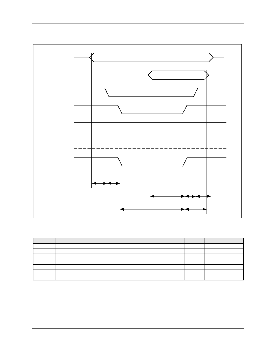
CX82100 Home Network Processor Data Sheet
5-6
Conexant Proprietary and Confidential Information
101306C
Figure 5-3. Waveforms for Host Master Mode Read Operation (CX82100-11/-12/-51/-52)
100603_017
Tpw
Tds
Tdh
Tas
Tcsh
HDS#
Tcss
HD[15:0]
HCS[X]#
HRD#
HW R#
HA[21:1]
HR/W #
address
data
Tah
Table 5-3. Timing for Host Master Mode Read Operation Based on a 100 MHz BCLK (CX82100-11/-12/-51/-52)
Symbol
Parameter
Min.
Max.
Units
Tas
Programmable address setup to active read
10
160
ns
Tpw
Programmable read pulse width
10
320
ns
Tds
Required data setup to end of active read
5
--
ns
Tdh
Required data hold time following active read
40
240
ns
Tah
Programmable address hold time following active read
40
90
ns
Tcsh
Programmable chip select hold time relative to RE# or R/W#
0
150
ns
Tcss
Programmable chip select setup time relative to RE# or R/W#
0
150
ns
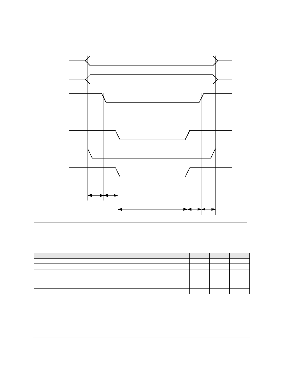
CX82100 Home Network Processor Data Sheet
101306C
Conexant Proprietary and Confidential Information
5-7
Figure 5-4. Waveforms for Host Master Mode Write Operation (CX82100-11/-12/-51/-52)
101603_018
Tpw
Tas
Tcsh
HDS#
Tcss
HD[15:0]
HCS[X]#
HRD#
HW R#
HA[21:1]
HR/W #
address
Tadh
data
Table 5-4. Timing for Host Master Mode Write Operation Based on a 100 MHz BCLK (CX82100-11/-12/-51/-52)
Symbol
Parameter
Min.
Max.
Units
Tas
Programmable address setup to active write
10
160
ns
Tpw
Programmable read pulse width
10
320
ns
Tadh
Programmable address and data hold time following active write (address
hold time is longer that data hold time so min. and max. is based on the
address hold time).
50
200
ns
Tcsh
Programmable chip select hold time relative to WE# or R/W#
0
150
ns
Tcss
Programmable chip select setup time relative to WE# or R/W#
0
150
ns

CX82100 Home Network Processor Data Sheet
5-8
Conexant Proprietary and Confidential Information
101306C
5.1.6
Host Master Mode Timing (CX82100-41/-42)
Host Master Mode Read Operation (Accessing an External Device)
The Host Master Mode read timing is illustrated in Figure 5-5 and listed in Table 5-5.
∑ HRD# and HWR# signals are used when the appropriate bit of the Host Master
Mode Transfer Control Register is low.
∑ HR/W# and HDS# signals are used when the appropriate bit of Host Master Mode
Transfer Control Register is high.
∑ Tpw is programmable via the Host Master Mode Read Wait-State Control registers
(HST_RWST).
∑ HRDY# is used for handshaking when the appropriate bit of the Host Master Mode
Peripheral Handshake register is set.
Host Master Mode Write Operation (Accessing an External Device)
The Host Master Mode write timing is illustrated in Figure 5-6 and listed in Table 5-6.
∑ HRD# and HWR# signals are used when the appropriate bit of the Host Master
Mode Transfer Control Register is low.
∑ HR/W# and HDS# signals are used when the appropriate bit of Host Master Mode
Transfer Control Register is high.
∑ Tpw is programmable via the Host Master Mode Write Wait-State Control registers
(HST_WWST).
∑ HRDY# is used for handshaking when the appropriate bit of the Host Master Mode
Peripheral Handshake register is set.

CX82100 Home Network Processor Data Sheet
101306C
Conexant Proprietary and Confidential Information
5-9
HRDY# Description (CX82100-41/-42)
HRDY# is used to extend a Host Interface operation. The use of HRDY# can be enabled
or disabled by setting or clearing the corresponding HRDY# Handshake Enable bit in the
MSTR_HANDSHAKE register (0x002D0024).
When HRDY# is enabled, the polarity of HRDY# can be programmed by setting or
clearing bit 0 of the MSTR_HANDSHAKE register.
∑ With HRDY# Polarity low (default polarity, bit 0 of 0x002D0024 = 0), HRDY# low
indicates the target on the Host Bus is ready/waiting and HRDY# high indicates the
target is busy. In this case, chip selects HCS0#-HCS5# will assert when HRDY# is
low and will not assert when HRDY# is high.
∑ With HRDY# Polarity high (bit 0 of 0x002D0024 = 1), HRDY# high indicates the
target on the Host Bus is ready/waiting and HRDY# low indicates the target is busy.
In this case, chip selects HCS0#-HCS5# will assert when HRDY# is high and will
not assert when HRDY# is low.
When HRDY# is enabled, the pulse widths of HRD# and HWR# are controlled by either
the HRDY# signal or the timing specified by the Host Read/Write Wait State Control
Register, whichever has longer cycle time. HRD# and HWR# will never have a smaller
width than the programmed values thus minimum Host Interface cycle time is
guaranteed.
When HRDY# is disabled, the state of HRDY# is ignored and the timing of the host
interface control and data signals are controlled by the timing configuration registers:
HST_RWST, HST_WWST, HST_READ_CNTL1, HST_READ_CNTL2,
HST_WRITE_CNTL1, and HST_WRITE_CNTRL2.
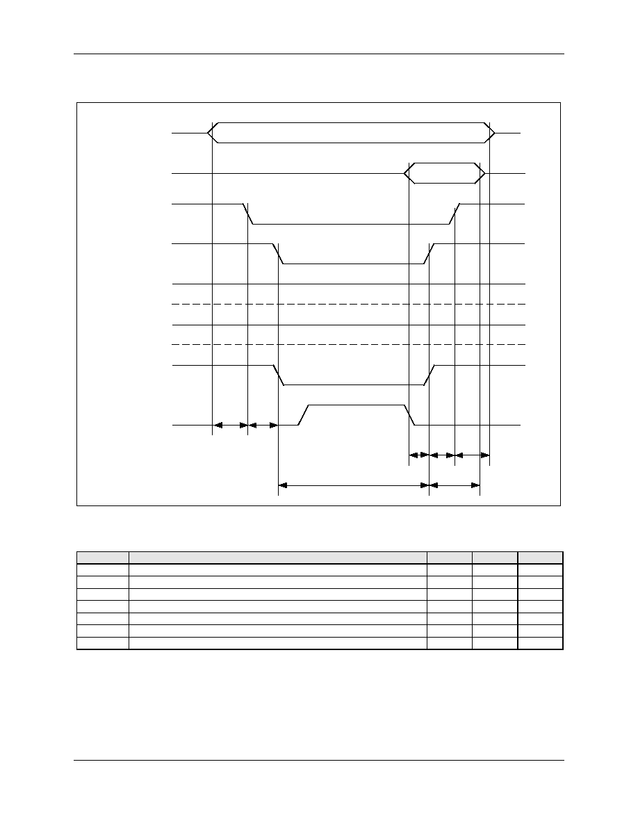
CX82100 Home Network Processor Data Sheet
5-10
Conexant Proprietary and Confidential Information
101306C
Figure 5-5. Waveforms for Host Master Mode Read Operation (CX82100-41/-42)
100545_079
Tpw
Tds
Tdh
Tas
Tcsh
HDS#
HRDY#
Tcss
HD[15:0]
HCS[X]#
HRD#
HWR#
HA[21:1]
HR/W#
address
data
Tah
Table 5-5. Timing for Host Master Mode Read Operation Based on a 100 MHz BCLK (CX82100-41/-42)
Symbol
Parameter
Min.
Max.
Units
Tas
Programmable address setup to active read
10
160
ns
Tpw
Programmable read pulse width
10
320
ns
Tds
Required data setup to end of active read
5
--
ns
Tdh
Required data hold time following active read
40
240
ns
Tah
Programmable address hold time following active read
40
90
ns
Tcsh
Programmable chip select hold time relative to RE# or R/W#
0
150
ns
Tcss
Programmable chip select setup time relative to RE# or R/W#
0
150
ns
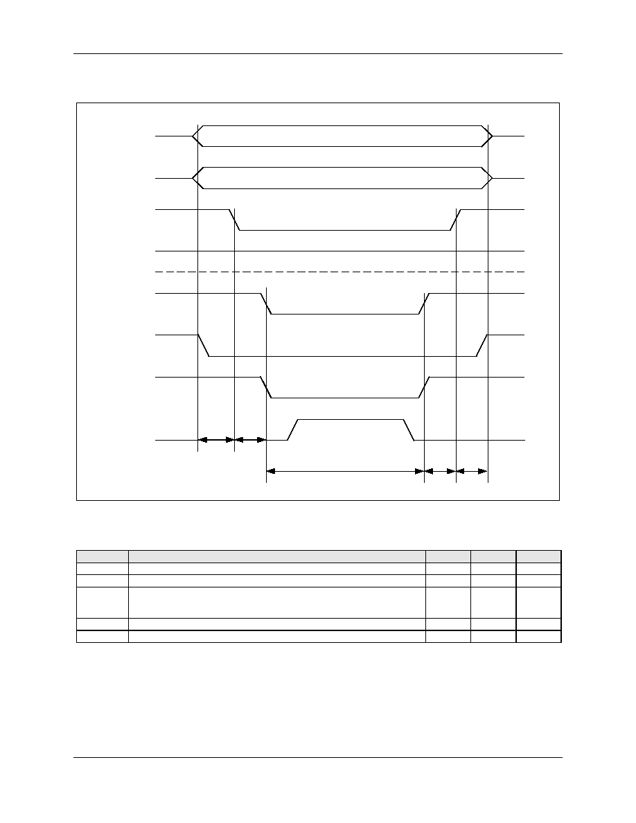
CX82100 Home Network Processor Data Sheet
101306C
Conexant Proprietary and Confidential Information
5-11
Figure 5-6. Waveforms for Host Master Mode Write Operation (CX82100-41/-42)
101545_080
Tpw
Tas
Tcsh
HDS#
HRDY#
Tcss
HD[15:0]
HCS[X]#
HRD#
HWR#
HA[21:1]
HR/W#
address
Tadh
data
Table 5-6. Timing for Host Master Mode Write Operation Based on a 100 MHz BCLK (CX82100-41/-42)
Symbol
Parameter
Min.
Max.
Units
Tas
Programmable address setup to active write
10
160
ns
Tpw
Programmable read pulse width
10
320
ns
Tadh
Programmable address and data hold time following active write (address
hold time is longer that data hold time so min. and max. is based on the
address hold time).
50
200
ns
Tcsh
Programmable chip select hold time relative to WE# or R/W#
0
150
ns
Tcss
Programmable chip select setup time relative to WE# or R/W#
0
150
ns
CX82100 Home Network Processor Data Sheet
5-12
Conexant Proprietary and Confidential Information
101306C
5.2
Host Master Mode Register Memory Map
Host Master Mode registers are identified in Table 5-7.
Table 5-7. Host Master Mode Registers
Register Label
Register Name
ASB Address
Type
Default Value
Ref.
HST_CTRL
Host Control Register
0x002D0000
RW
0x00000008
5.3.1
HST_RWST
Host Master Mode Read-Wait-State Control
Register
0x002D0004
RW
0x00739CE7
5.3.2
HST_WWST
Host Master Mode Write-Wait-State Control
Register
0x002D0008
RW
0x00739CE7
5.3.3
HST_XFER_CNTL
Host Master Mode Transfer Control Register
0x002D000C
RW
0x00000000
5.3.4
HST_READ_CNTL1
Host Master Mode Read Control Register 1
0x002D0010
RW
0x00000000
5.3.5
HST_READ_CNTL2
Host Master Mode Read Control Register 2
0x002D0014
RW
0x00000000
5.3.6
HST_WRITE_CNTL1
Host Master Mode Write Control Register 1
0x002D0018
RW
0x00000000
5.3.7
HST_WRITE_CNTL2
Host Master Mode Write Control Register 2
0x002D001C
RW
0x00000000
5.3.8
MSTR_INTF_WIDTH
Host Master Mode Peripheral Size
0x002D0020
RW
0x00000000
5.3.9
MSTR_HANDSHAKE
Host Master Mode Peripheral Handshake
0x002D0024
RW
0x00000000
5.3.10
HDMA_SRC_ADDR
Host Master Mode DMA Source Address
0x002D0028
RW
0x00000000
5.3.11
HDMA_DST_ADDR
Host Master Mode DMA Destination Address
0x002D002C
RW
0x00000000
5.3.12
HDMA_BCNT
Host Master Mode DMA Byte Count
0x002D0030
RW
0x00000000
5.3.13
HDMA_TIMERS
Host Master Mode DMA Timers
0x002D0034
RW
0x00000000
5.3.14

CX82100 Home Network Processor Data Sheet
101306C
Conexant Proprietary and Confidential Information
5-13
5.3
Host Master Mode Registers
5.3.1
Host Control Register (HST_CTRL: 0x002D0000)
Bit(s)
Type
Default
Name
Description
31:12
Reserved.
11
R/W
1'b0
DMA_SRC_ADDR_INC_DISABLE
Disable DMA Source Address Increment.
0 = Enable DMA Source Address Increment.
1 = Disable DMA Source Address Increment.
10
R/W
1'b0
DMA_DST_ADDR_INC_DISABLE
Disable DMA Destination Address Increment.
0 = Enable DMA Destination Address Increment.
1 = Disable DMA Destination Address Increment.
9:8
RW
2'b00
HDMA_MODE_SEL
Host Master Mode DMA Transfer Mode Select.
00 =
Asynchronous DMA Mode.
01 =
Reserved.
10 =
Isochronous DMA Mode using internal timer.
11 =
Reserved.
7
Reserved.
6
RW
1'b0
EN_BLOCK_ARM
Enable the arbiter to lock 940 ADR/SEQ/ and Bursts.
0 = Disable arbiter to lock 940 ADR/SEQ/ and Bursts.
1 = Enable arbiter to lock 940 ADR/SEQ/ and Bursts.
5
Reserved.
4
RW
1'b0
RUN_MAP
Run-Time Memory Map.
0 = Flash ROM @ starting address 0x00000000,
internal RAM @ starting address 0x00180000.
1 = Internal RAM @ starting address 0x00000000,
Flash ROM @ starting address 0x00180000.
3:2
RW
2'b10
XDM_SZ
External Dynamic Memory Size.
00 =
2 MB.
01 =
4 MB.
10 =
8 MB.
11 =
Reserved.
1:0
RW
2'b00
HST_HIRQ
HIRQ0# Output State for External Host.
0x =
Off.
10 =
Asserted low.
11 =
De-asserted and pulled high.

CX82100 Home Network Processor Data Sheet
5-14
Conexant Proprietary and Confidential Information
101306C
5.3.2
Host Master Mode Read-Wait-State Control Register (HST_RWST: 0x002D0004)
Bit(s)
Type
Default
Name
Description
31:25
Reserved.
24:20
RW
5'b00111
HST_RWS4
HCS4 Wait State Control for Master Mode Read Cycles.
Length of read cycle = count value * 1 BCLK period + 1 BCLK period.
19:5
Reserved.
4:0
RW
5'b00111
HST_RWS0
HCS0 Wait State Control for Master Mode Read Cycles.
Length of read cycle = count value * 1 BCLK period + 1 BCLK period.
5.3.3
Host Master Mode Write-Wait-State Control Register) (HST_WWST: 0x002D0008)
Bit(s)
Type
Default
Name
Description
31:25
Reserved.
24:20
RW
5'b00111
HST_WWS4
HCS4 Wait State Control for Master Mode Write Cycles.
Length of read cycle = count value * 1 BCLK period + 1 BCLK period.
19:5
Reserved.
4:0
RW
5'b00111
HST_WWS0
HCS0 Wait State Control for Master Mode Write Cycles.
Length of read cycle = count value * 1 BCLK period + 1 BCLK period.
5.3.4
Host Master Mode Transfer Control Register (HST_XFER_CNTL: 0x002D000C)
Bit(s)
Type
Default
Name
Description
31:8
Reserved.
7
RW
1'b0
Hcs4_ds_polarity
HCS4 External Data Strobe Polarity.
0 = Negative data strobe polarity.
1 = Positive data strobe polarity.
6:4
Reserved.
3
RW
1'b0
Hcs4_xfer_mode
HCS4 External Transfer Mode.
0 = WE# and RE# transfer mode.
1 = R/W# and DS# transfer mode.
2:0
Reserved.
5.3.5
Host Master Mode Read Control Register 1 (HST_READ_CNTL1: 0x002D0010)
Bit(s)
Type
Default
Name
Description
31:28
RW
4'b0
HRcs4_Tcss
HCS4 Chip Select Setup Time Relative to RE# or R/W#.
Length = count value * 1 BCLK period.
27:16
Reserved.
15:12
RW
4'b0
HRcs4_Tcsh
HCS4 Chip Select Hold Time Relative to RE# or R/W#.
Length = count value * 1 BCLK period.
11:0
Reserved.

CX82100 Home Network Processor Data Sheet
101306C
Conexant Proprietary and Confidential Information
5-15
5.3.6
Host Master Mode Read Control Register 2 (HST_READ_CNTL2: 0x002D0014)
Bit(s)
Type
Default
Name
Description
31:28
RW
4'b0
HRcs4_Tas
HCS4 Address Setup Time to Active Read.
Length = count value * 1 BCLK period + 1 BCLK period.
27:16
Reserved.
15:12
RW
4'b0
HRcs4_Tah
HCS4 and HCS5 Address Hold Time Following Active Read.
Length
count value * 1 BCLK period + 4 BCLK periods.
11:0
Reserved.
5.3.7
Host Master Mode Write Control Register 1 (HST_WRITE_CNTL1: 0x002D0018)
Bit(s)
Type
Default
Name
Description
31:28
RW
4'b0
HWcs4_Tcss
HCS4 Chip Select Setup Time Relative to WE# or R/W#.
Length = count value * 1 BCLK period.
27:16
Reserved.
15:12
RW
4'b0
HWcs4_Tcsh
HCS4 Chip Select Hold Time Relative to WE# or R/W#.
Length = count value * 1 BCLK period.
11:0
Reserved.
5.3.8
Host Master Mode Write Control Register 2 (HST_WRITE_CNTL2: 0x002D001C)
Bit(s)
Type
Default
Name
Description
31:28
RW
4'b0
HRcs4_Tas
HCS4 Address Setup Time to Active Write.
Length = count value * 1 BCLK period + 1 BCLK period.
27:16
Reserved.
15:12
RW
4'b0
HRcs4_Tadh
HCS4 Address and Data Hold Time Following Active Write.
For data, Length = count value * 1 BCLK period + 1 BCLK period.
For address, Length
count value * 1 BCLK period + 5 BCLK periods.
11:0
Reserved.
5.3.9
Host Master Mode Peripheral Size (MSTR_INTF_WIDTH: 0x002D0020)
Bit(s)
Type
Default
Name
Description
31:5
Reserved.
4
RW
1'b0
Mstr_intf_width4
HCS4 Data Length.
0 = 16-bit data length.
1 = 8-bit data length.
3:0
Reserved.

CX82100 Home Network Processor Data Sheet
5-16
Conexant Proprietary and Confidential Information
101306C
5.3.10
Host Master Mode Peripheral Handshake (MSTR_HANDSHAKE: 0x002D0024)
(CX82100-41/-42)
Bit(s)
Type
Default
Name
Description
31:5
Reserved.
4
RW
1'b0
Mstr_handshake4
HCS4 HRDY# Handshake Enable.
0 = Disable HRDY# handshake.
1 = Enable HRDY# handshake.
3:1
Reserved.
0
RW
1'b0
Mstr_handshake0
HRDY# Polarity.
0 = Active low
1 = Active high
5.3.11
Host Master Mode DMA Source Address (HDMA_SRC_ADDR: 0x002D0028)
Bit(s)
Type
Default
Name
Description
31:24
Reserved.
23:0
RW
24'b0
HDma_source_addr
Least significant 24 bits of the address of the first byte of DMA source
data.
5.3.12
Host Master Mode DMA Destination Address (HDMA_DST_ADDR: 0x002D002C)
Bit(s)
Type
Default
Name
Description
31:24
Reserved.
23:0
RW
24'b0
HDma_dest_addr
Least significant 24 bits of the first location of the DMA destination.
5.3.13
Host Master Mode DMA Byte Count (HDMA_BCNT: 0x002D0030)
Bit(s)
Type
Default
Name
Description
31:22
Reserved.
21:0
RW
22'b0
HDma_byte_count
The number of bytes of data to be transferred via the host DMA.
5.3.14
Host Master Mode DMA Timers (HDMA_TIMERS: 0x002D0034)
Bit(s)
Type
Default
Name
Description
31:16
Reserved.
15:8
RW
8'b0
HDMA_ISOC_TIMER
Timer which dictates the transfer rate for an isochronous mode
DMA transfer in terms of the number of BCLK periods.
7:0
RW
8'b0
HDMA_INACTIVE_TIMER
The minimum interval, in terms of number of BCLK periods,
between subsequent accesses to an external DMA source or
destination.
CX82100 Home Network Processor Data Sheet
101306C
Conexant Proprietary and Confidential Information
6-1
6
External Memory Controller Interface Description
6.1
PC100 Compliant SDRAM Interface
The External Memory Controller (EMC) provides a 16-bit interface to support up to 8
MB of external SDRAM. Figure 6-1 shows a typical SDRAM functional block diagram.
Note that the actual SDRAM design varies from vendor to vendor. Figure 6-1 also shows
an Intel PC100 compliant interface between the EMC and the SDRAM. Table 6-1 lists
the definition for each interface signal. A PC100 compliant SDRAM must also support a
mode register whose functions are defined in Table 6-2. The mode register is
programmable through the MRS (Mode Register Set) command defined in the PC100
Specification (see Reference [6]).
Figure 6-1. SDRAM Interface
101545_025
Data I/O +
Control
Logic
RA
Decode +
Control
Logic
Control Logic
Command
Refresh
Bank
Banks
(2x or 4x)
Mode register
CA
Decode +
Control
Logic
External
Mem ory
Controller
MM[1:0]
MD[15:0]
ASB
MB[1:0]
MA[11:0]
MRAS#
MCAS#
MW E#
MCS#
MCKE
MCLK
SDRAM
HNP

CX82100 Home Network Processor Data Sheet
6-2
Conexant Proprietary and Confidential Information
101306C
Table 6-1. EMC SDRAM Interface Signal Descriptions
Pin Name
I/O
Signal Name
Description
MD[15:0]
I/O
Memory Data
Bi-directional data access bus for DRAM.
MA[11:0]
O
Memory Address
Multiplexed row and column address for access of data up to 8 MB.
MB[1:0]
O
Bank Address
Selects active memory bank.
MM[1:0]
O
Memory Mask
Input mask signal for write accesses.
MRAS#
O
Row Address Strobe
Starts SDRAM access with strobe of row address.
MCAS#
O
Column Address
Strobe
Strobes column address and data bytes.
MWE#
O
Memory Write Enable
Indicates write access to SDRAM.
MCS#
O
Memory Chip Select
Enables the SDRAM command decoder.
MCKE
O
Memory Clock Enable
Memory Clock activation.
MCLK
O
Memory Clock
All SDRAM signals sampled on positive edge.
Table 6-2. PC100 Compliant Mode Register
Bit No.
Name
Supported Function
11:7
Reserved.
6:4
LTMODE
CAS# Latency.
011 =
3 cycles.
All Other =
Reserved.
3
WT
Wrap Type.
0 = Linear.
1 = Interleave.
2:0
BL
Burst Length.
011 =
8 cycles.
All Other =
Reserved.
The SDRAM clock runs at 100 MHz, however, 125 MHz rated SDRAM is required in
order to guarantee setup time margin.

CX82100 Home Network Processor Data Sheet
101306C
Conexant Proprietary and Confidential Information
6-3
6.2
Available Vendor SDRAM ICs and Features
Although the EMAC is not fully PC100 compliant due to the fact that both the CAS#
latency and the burst length are hard wired, many other PC100 compliant vendor
SDRAMs are usable for the EMAC design. Table 6-3 lists some of these SDRAMs and
their corresponding features and access timings.
Table 6-3. Available SDRAM Vendors
1M x 16 x 4 SDRAM
Input
Output
Initialization
Sequence
Spec./
Vendor
Basic
Features
Ref.
Rate
Clock
Cycle
Setup
Hold
Valid
Hold
Valid to Z
Intel
PC100 Spec.
(Rev. 1.63)
CL = 2,3
BL = 1,2,4
Burst Read
Burst Write
Auto Refresh
Period: 10 ns
High: 3 ns
Low: 3 ns
2 ns
1 ns
CL = 3: 6 ns
C
L
= 2: 6 ns
3 ns
Min: 3 ns
Max: 9 ns
200
µ
s -> Precharge ->
8RF -> MRS-> 1st
Command
Micron
MT48LC4M16A2
CL = 1,2,3
BL = 1,2,4,8,FP
Burst Read
Burst Write
Single Write
Auto Refresh
Self Refresh
15.6
µ
s
CL = 3: 8 ns
CL = 2: 10 ns
2 ns
1 ns
CL = 3: 6 ns
CL = 2: 6 ns
1.8 ns CL = 3: 6 ns
CL = 2: 7 ns
100
µ
s -> Precharge ->
2RF min -> MRS -> 1st
Command
Samsung
KM416S4030D
CL = 2,3
BL = 1,2,4,8,FP
Burst Read
Burst Write
Auto Refresh
Self Refresh
15.6
µ
s
Period: 10 ns
2 ns
1 ns
CL = 3: 6 ns
CL = 2: 6 ns
3 ns
CL = 3: 6 ns
CL = 2: 7 ns
100
µ
s -> Precharge ->
2RF min -> MRS-> 1st
Command
Fujitsu
MB81F641642D
CL = 2,3
BL = 2,4,8,FP
Burst Read
Burst Write
Single Write
Auto Refresh
Self Refresh
15.6
µ
s
Period: 10 ns
High: 3 ns
Low: 3 ns
2 ns
1 ns
CL = 3: 6 ns
CL = 2: 6 ns
3 ns
Min: 3 ns
Max: 6 ns
100
µ
s -> Precharge ->
2RF min -> MRS-> 1st
Command
NEC
PD4564841-10
CL = 2,3
BL = 1,2,4,8,FP
Burst Read
Single Write
Auto Refresh
Self Refresh
15.6
µ
s
CL = 3: 10 ns
CL = 2: 13 ns
High: 3 ns
Low: 3 ns
2 ns
1 ns
CL = 3: 6 ns
CL = 2: 7 ns
3 ns
CL = 3: 6 ns
CL = 2: 7 ns
Min: 3 ns
200
µ
s -> Precharge ->
2RF min -> MRS-> 1st
Command
IBM
19L3264-10
CL = 2,3
BL = 1,2,4,8,FP
Burst Read
Single Write
Auto Refresh
Self Refresh
15.6
µ
s
CL = 3: 10 ns
CL = 2: 15 ns
3 ns
1 ns
CL = 3: 7 ns
CL = 2: 8 ns
3 ns
Min: 3 ns
Max: 7 ns
200
µ
s -> Precharge ->
8RF -> MRS-> 1st
Command
Toshiba
TC59S6416BFT-
10
CL = 2,3
BL = 1,2,4,8,FP
Burst Read
Single Write
Auto Refresh
Self Refresh
15.6
µ
s
10 ns
2.5 ns
1 ns
7 ns
3 ns
Min: 3 ns
Max: 10 ns
200
µ
s -> Precharge ->
8RF -> MRS-> 1st
Command
CX82100 Home Network Processor Data Sheet
6-4
Conexant Proprietary and Confidential Information
101306C
6.3
Supported Configurations
Table 6-4 lists supported SDRAM configurations. There are only one or two memory ICs
at most that reside on the external SDRAM bus (e.g., two 2M x 8 SDRAMs are required
to get 4 MB). This bus is not shared with any other external function. Since the EMC
buffers write data phases, this pipelined activity implies that the SDRAM bus can be busy
concurrently with asynchronous and independent host bus transfers. (An external host can
read/write SDRAM as well.)
Table 6-4. Allowed SDRAM Configurations
Total
Memory
Memory
Config.
No. of
SDRAMs
SDRAM
Config.
SDRAM
Capacity
SDRAM
No. of
Banks
SDRAM
No. of
Rows
SDRAM
No. of
Columns
2 MB
1Mb x 16
1
1Mb x 16
16 Mb
2
2Kb
256
4 MB
2Mb x 16
2
2Mb x 8
16 Mb
2
2Kb
512
8 MB
4Mb x 16
1
4Mb x 16
64 Mb
4
4Kb
256
6.4
Access Cycles
The EMC's SDRAM 16-bit interface is synchronous. All of the SDRAM inputs are
registered on the positive edge of MCLK. The SDRAM uses an internal pipelined
architecture to achieve high-speed operation. Read and write accesses to the SDRAM are
burst oriented (it's been noted from the simulation that the EMAC design only allows
read accesses to the SDRAM to be burst oriented). A burst of 8 allows a cache line (16
bytes) to be refilled in one single read. Accesses begin with the registration of an
ACTIVE command, which is then followed by a READ or WRITE command.
6.5
Initialization
The SDRAM requires a 200
µs delay prior to applying an executable command. The
delay begins after reset when power and clock are stable. The microcontroller should not
access the SDRAM during this time, otherwise all processes will be held up while the
EMC inserts wait states for the full initialization duration. No user intervention is
required during the initialization process. All appropriate settings are managed by the
SDRAM controller.
6.6
Refresh
The SDRAM controller supports Auto-Refresh. Refresh requests are generated to meet a
15.625
µs per row interval (to be safe, it is preferable that refresh requests could be
generated at a rate less than 15.625
µs per row interval). Refresh cycles are transparent to
the host, but will insert wait cycles if the memory is accessed during a refresh request.
Refresh requests have top priority when accessing the memory. Refresh cycles will not
interrupt a memory cycle in process.
CX82100 Home Network Processor Data Sheet
101306C
Conexant Proprietary and Confidential Information
6-5
6.7
Read
No acceleration is provided for read accesses. Multiple memory banks allow multiple
rows to be active simultaneously. This reduces the need for precharge and activate cycles,
allowing a faster aggregate throughput.
6.8
Write
A 2-dword buffer is provided to speed up random and DMA write accesses.
6.9
Throughput
Better than 114 MB/s for 16-byte cache-line fills and 177 MB/s for buffered 16-byte
writes. Random read or write single accesses operate at 50 MB/s and 200 MB/s,
respectively. Table 6-5 summarizes the throughput for each access type.
Table 6-5. SDRAM Throughput
16-bit SDRAM Interface
No. of BCLK Cycles
32-bit Access
1 dword
4 dwords (Seq Burst)
Write
2
9
Read
8
14
Write immediately following Write
2
15
Read immediately following Read
12
18
16-bit Access
1 word
4 words (Seq Burst)
Write
2
8
Read
7
10
Write immediately following Write
2
11
Read immediately following Read
12
12
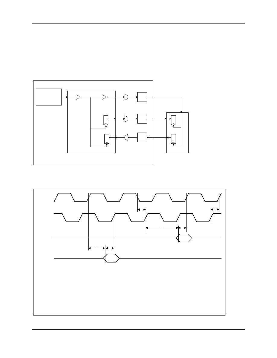
CX82100 Home Network Processor Data Sheet
6-6
Conexant Proprietary and Confidential Information
101306C
6.10
EMC I/O Clock Interface and Timing
The EMC I/O clock interface is illustrated in Figure 6-2.
The EMC I/O timing is illustrated in Figure 6-3.
Figure 6-2. EMC Clocking Interface
101545_026
CLKGEN
MODULE
PAD
BCLK
MCLK
ext_sdram
asb_sdram
D
Q
PAD
MD
HNP
PAD
MA
D
Q
BCLK
scan m ux
scan mux
scan mux
MCLK
MA
MD
Figure 6-3. EMC I/O Timing
101545_027
BCLK
M CLK
DATA
M D
ADDR
M A
A = tck-q + tdsm + tpo
B = tasu
C = clock skew = tdi + tdsm + tpo
D = ta
E = tsu + tpi + tdsm
F = (clk period / 2) - tdi - tdsm - tpo
Notes:
W here:
A
B
C
D
E
F
tck-q = asb_sdram flop clk-q delay
tsu = asb_sdram flop setup tim e
th = asb_sdram flop hold tim e
tdsm = HNP scan m ux delay
tpo = output pad delay
tpi = input pad delay
tdi = HNP inverter delay
ta = sdram read access tim e
CX82100 Home Network Processor Data Sheet
101306C
Conexant Proprietary and Confidential Information
6-7
6.11
SRAM Interface
The HNP EMC can alternatively interface to SRAM memory. The SDRAM associated
pins are used for this interface and are multiplexed to either interface to SDRAM or
SRAM. SDRAM or SRAM interface is controlled by the EMCR register and allows for
different external sizes and up to two SRAM devices. Using two 512-kbyte SRAM
devices (256k x 16 each), a maximum of 1 MB of external SRAM can be achieved. The
EMCR register controls for SRAM read/write wait state control, selection of one or two
memory chips, and selection of various sizes for each of the memories.
The SDRAM-to-SRAM signal mapping is shown in Table 6-6.
If one SRAMs are used, connect CE_SRAM1# to the SRAM CE# (Chip Enable) and
leave CE_SRAM2# open.
If two SRAMs are used, connect CE_SRAM1# to the lower address range SRAM
(SRAM 1) CE# and CE_SRAM2# to the upper address range SRAM (SRAM 2) CE#.
For the SRAMs, connect OE# (Output Enable), BLE# (Byte Low Enable), and BHE#
(Byte High Enable) to VSS.
Table 6-6. HNP to SDRAM/SRAM Interface Signal Mapping
HNP Pin Signal
SDRAM Interface
SRAM Pin Signal
MCKE
CKE
A17
MCAS#
MCAS#
A16
MB1
MB1
A15
MB0
MB0
A14
MM1
MM1
A13
MM0
MM0
A12
MA[11:0]
A[11:0]
A[11:0]
MD[15:0]
D[15:0]
IO[15:0]
MCS#
CS#
CE# (SRAM 1)
MRAS#
RAS#
CE# (SRAM 2)
MWE#
WE#
WE#

CX82100 Home Network Processor Data Sheet
6-8
Conexant Proprietary and Confidential Information
101306C
6.12
EMC Register
The EMC register is identified in Table 6-7.
Table 6-7. EMC Register
Register Label
Register Name
ASB Address
Type
Default Value
Ref.
EMCR
External Memory Control Register
0x00350010
RW
0x00000000
6.12.1
6.12.1
External Memory Control Register (EMCR: 0x00350010)
Bit(s)
Type
Default
Name
Description
7:6
RW
2'b00
SRWSC
SRAM Read/Write Wait State Control.
00 =
No extra delay.
01 =
Delayed by one BCLK period.
10 =
Delayed by two BCLK periods.
11 =
Delayed by three BCLK periods.
Note: The delay cycles are extra to the normal access cycles.
5:4
RW
2'b00
SRCSEL2
SRAM Chip Select 2.
00 =
Do not select the second SRAM chip.
01 =
Select the second SRAM chip, size = 64K x 16.
10 =
Select the second SRAM chip, size = 128K x 16.
11 =
Select the second SRAM chip, size = 256K x 16.
Notes:
1.
EXMSEL must be 2'b10 if the second SRAM chip is selected.
2.
The size for the second SRAM must be no greater than the size
of the first SRAM.
3.
If the second SRAM size is programmed at a value greater than
that of the first SRAM, then the actual size for the second SRAM
will be reduced to the same size as the first automatically by the
hardware.
3:2
RW
2'b00
SRCSEL1
SRAM Chip Select 1.
00 =
Do not select the first SRAM chip.
01 =
Select the first SRAM chip, size = 64K x 16.
10 =
Select the first SRAM chip, size = 128K x 16.
11 =
Select the first SRAM chip, size = 256K x 16.
Note: EXMSEL must be 2'b10 if the first SRAM chip is selected.
1:0
RW
2'b00
EXMSEL
External Memory Select.
00 =
Select SDRAM interface; SDRAM in Disabled Mode.
01 =
Select SDRAM interface; SDRAM in Enabled Mode.
10 =
Select SRAM interface.
11 =
Reserved.
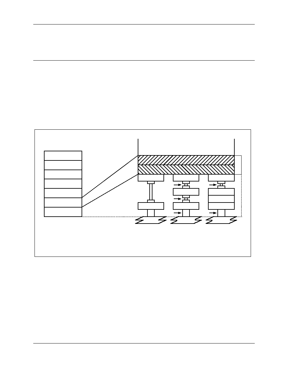
CX82100 Home Network Processor Data Sheet
101306C
Conexant Proprietary and Confidential Information
7-1
7
Ethernet Media Access Control Interface Description
The HNP implements the Ethernet Media Access Control (EMAC) as defined in
Reference [4]. Also implemented is the MII interface to the physical layer as defined in
Reference [5].
In the OSI reference model as shown in Figure 7-1, the lowest layer is Physical and the
next layer up is Data Link. The Data Link layer is segmented into 2 parts, Medium
Access Control (MAC) which interfaces to the PHY, and the Logical Link Control (LLC)
which interfaces to the MAC and to higher layers.
Figure 7-1. MAC Sublayer Partition, Relationship to OSI Reference Model
101545_028
Reconciliation
PMA
PLS
Reconciliation
PMA
PLS
PMD
Physical
Network
Transport
Session
Presentation
Application
Data Link
PMA
OSI Reference M odel
Layers
LAN CSM A/CD Layers
Higher Layers
AUI
1 Mb/s, 10 Mb/s
10 Mb/s
100 Mb/s
AUI = Attachm ent Unit Interface
MDI = Medium Dependent Interface
MII = Media Independent Interface
PLS = Physical Layer Signaling
PMA = Physical Medium Attachm ent
PMD = Physical Medium Dependent
PLS
Medium
Medium
Medium
MII
MII
MDI
MDI
LLC - Logical Link Control
M AC - M edia Access Control
The LLC together with the MAC must provide the following Data Link functionality:
∑ Data Encapsulation (transmit and receive)
- Framing (frame boundary delimitation, frame synchronization)
- Addressing (handling of source and destination addresses)
∑ Error detection (detection of physical medium transmission errors)
- Media Access Management
- Medium Allocation (collision avoidance)
- Contention Resolution (collision handling)
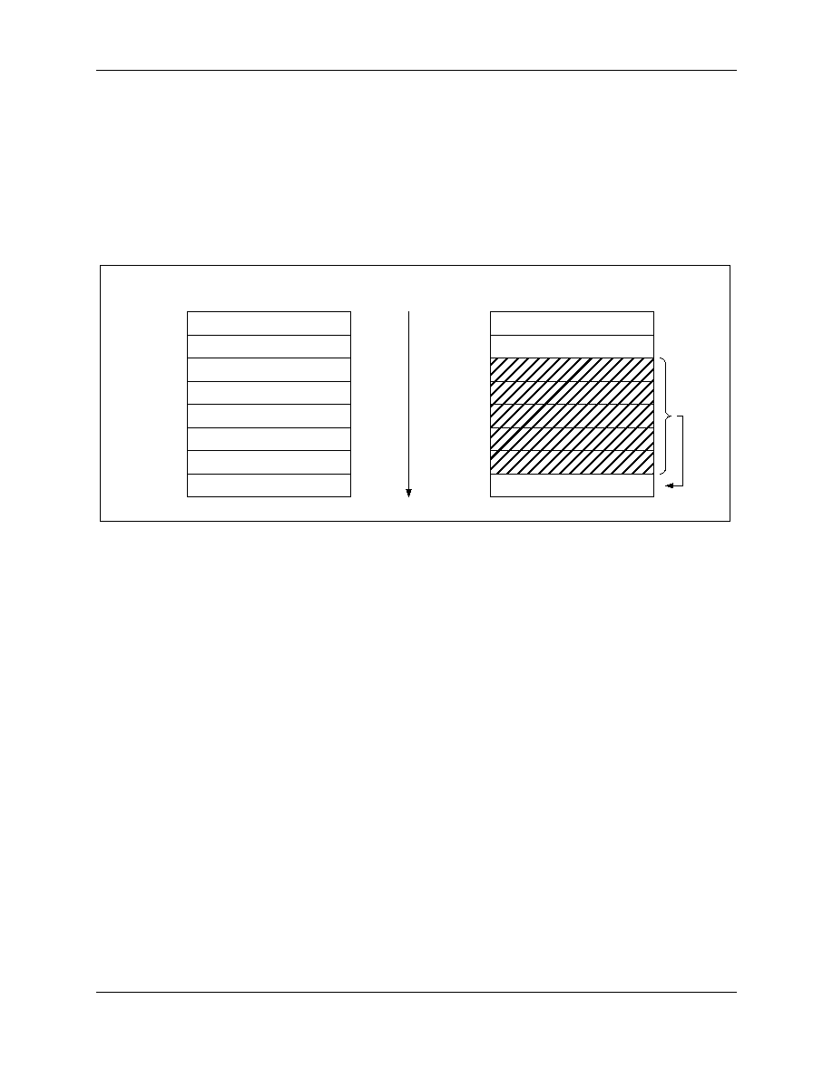
CX82100 Home Network Processor Data Sheet
7-2
Conexant Proprietary and Confidential Information
101306C
7.1
MAC Frame Format
Figure 7-2 shows the MAC frame format supported by the HNP (see Section 3.1.1 of
Reference [4]). As depicted in the figure, the bytes of a frame are transmitted from top to
bottom. The bits of each byte in each field (with the exception of the FCS) are
transmitted from the LSb to MSb (i.e., LSb transmitted first).
Figure 7-2. Ethernet MAC Frame Format
101545_029
Pream ble
LLC Data
Length
Source Address (SA)
Destination Address (DA)
Start Fram e Delim iter (SFD)
Fram e Check Sequence (FCS)
PAD
2 or 6 Bytes
7 Bytes
2 or 6 Bytes
1 Byte
2 Bytes
(variable)
(variable)
4 Bytes
B
y
te
s
W
i
th
in
F
r
a
m
e
T
r
a
n
s
m
i
tte
d
fro
m
T
o
p
-
to
-B
o
tto
m
Defined in Standard
Pream ble
LLC Data
Length
Source Address (SA)
Destination Address (DA)
Start Fram e Delim iter (SFD)
Fram e Check Sequence (FCS)
PAD
6 Bytes
7 Bytes
6 Bytes
1 Byte
2 Bytes
(variable)
(variable)
4 Bytes
Implemented
F
i
el
ds i
n
v
o
l
v
ed i
n
F
C
S
C
o
m
put
a
t
i
o
n
At the head of the MAC frame is the 7-byte preamble 0xAA AA AA AA AA AA AA
followed by the 1-byte Start of Frame Delimiter (SFD) 0xAB. The MAC receiver must
detect the SFD pattern 0xAB. After SFD the MAC must begin receiving the frame
(assuming the Carrier Sense signal is asserted).
The address fields are the next fields in the frame. First is the 48-bit destination address
followed by the 48-bit source address. Then comes the 2-byte length field. Then comes
the LLC data and any pad bits required so the frame size is the minimum allowable
(which is 64 bytes not including FCS).
Finally, we have the 4 byte frame check sequence (FCS) which is a CRC to check for
frame errors due to Ethernet PHY (EPHY) transmission impairments. All fields except
the preamble, SFD, and FCS are used to compute the CRC. The CRC generating
polynomial is G(x) = X
32
+X
26
+X
23
+X
22
+X
16
+X
12
+X
11
+X
10
+X
8
+X
7
+X
5
+X
4
+X
2
+X+1.
The 32 bits of the CRC value are placed in the FCS field so that the X
31
term is the
leftmost bit of the first byte of the field, and the X
0
term is the rightmost bit of the last
byte of the field. The bits of the FCS field are thus transmitted in the order X
31
, X
30
, ...,
X
2
, X
1
, X
0
.

CX82100 Home Network Processor Data Sheet
101306C
Conexant Proprietary and Confidential Information
7-3
7.2
Parameterized Values Used in Implementation
Table 7-1 shows the values of the standard parameters used in the EMAC
implementation. These parameters are defined in sections 4.4.2.1 of Reference [4] and
4.4.2.3 of Reference [5]. The value specified for the Interframe Gap (IFG) parameter
determines the speed of the Ethernet. It is defined to be 96
µs for 1 Mb/s implementation,
9.6
µs for 10 Mb/s implementation, and 0.96 µs for 100 Mb/s implementation. Only the
10 Mb/s and 100 Mb/s implementations are supported in the HNP. The IFG parameter is
programmable through the Ethernet Network Access Register (bits 17:16 of E_NA_1 and
E_NA_2 for EMAC1 and EMAC2, respectively).
Table 7-1. Parameterized Values Implemented in EMAC
Parameter
Values
SlotTime
512 bit times
IFG (Interframe Gap)
programmable
AttemptLimit
16
BackoffLimit
10
JamSize
32 bits
MaxFrameSize
1518 bytes
MinFrameSize
512 bits (64 bytes)
AddressSize
48 bits

CX82100 Home Network Processor Data Sheet
7-4
Conexant Proprietary and Confidential Information
101306C
7.3
EMAC Functional Features
The EMAC block supports the MAC sublayer of the IEEE 802.3 and allows it to be
connected to an IEEE 802.3 10/100 Mbps (100BASE-T and 10BASE-T) MII compatible
EPHY device. The EMAC block supports the following features:
∑ For frame transmission
- Accepts data from host and constructs a frame
- Presents nibble data stream to the EPHY
∑ For frame reception
- Receives nibble data stream from the EPHY
- Presents to the host frames that are either broadcast/multicast frames or directly
addressed to the local station
- Discards or passes to the host all frames not addressed to it (programmable)
- Defers transmission whenever the medium is busy
- Delays transmission of frame for specified interframe gap (IFG) period
- Appends preamble, SFD, FCS to frames, and inserts PAD field for frames
whose data length is less than minFrameSize
- Halts transmission when collision is detected
- Enforces collision to ensure propagation throughout network by sending jam
message
- Schedules retransmission after a collision until attemptLimit is reached
- Checks received frames for transmission errors by way of FCS
- Discards received frames that are less than minFrameSize.
- Removes preamble and SFD. FCS and pad field (if necessary) from received
frames are passed along.
- IEEE 802.3u MII Physical Layer Interface
- Full-duplex or half-duplex operation
- Normal and internal loopback mode
- Linked list transmit data structures for scatter/gather support.
- Programmable data padding and FCS capability
- Address filtering (promiscuous, perfect, inverse and hash filtering)
- Programmable IFG
- Generates signals for software to maintain MIB (Management Information
Base) status in software
- Management Data Interface (MDI) to an MII compliant EPHY
- qword (64-bit) interface to the DMA controller
In half-duplex mode, the HNP checks the line condition before starting to transmit. If the
condition is clear, it starts transmitting (after IFG). Transmit enable (EMx_TXEN) asserts
and data is transferred through the MII port.

CX82100 Home Network Processor Data Sheet
101306C
Conexant Proprietary and Confidential Information
7-5
Full-duplex operation allows simultaneous transmission and reception of data, which can
effectively double data throughput to 20 or 200 Mb/s. In full-duplex mode, the HNP
starts transmitting a frame provided that IFG duration time has elapsed since its previous
transmission. Since there is no collision in full-duplex mode, the transmission always
ends successfully. The HNP monitors the line for a new frame transmission in both half
and full duplex modes. A new frame transmission is defined as both transmit data valid
and carrier sense asserted.
The following features of the EMAC should be taken into account:
∑ The FCS is defined as a 32-bit field, which means the minimum number of data
bytes required for a meaningful FCS is 4 (i.e. you can not generate a 32-bit FCS
from data that is shorter than 32-bits). Packets which are less than 4 bytes long,
should not be checked for FCS.
∑ Received EMAC frames are padded to align to qword boundaries, during
reception, prior to DMAC transfer. However, the length that is used in the length
status field is calculated prior to the padding insertion. This length field, FL, bits
31-16 of the RMAC in-line status qword, is provided in bytes. This length, FL,
includes the entire frame that was transmitted, including CRC, but it does not
include the padding bytes that were added by the EMAC receiver to align to the
qword boundary. The next frame is defined to start at the beginning of that same
qword boundary.
∑ Setting up the EMAC receiver for address filtering is done by directly
programming all filter related register bits (E_NA_HP, E_NA_HO, E_NA_IF,
E_NA_PR, and E_NA_PM) via writes to the E_NA register.
∑ If an RX FIFO overflow interrupt occurs, the RX should be reset via bit
E_NA_RRX in the E_NA register. The most recently written packet in the RX
circular buffer is damaged, and must be aborted by the software.
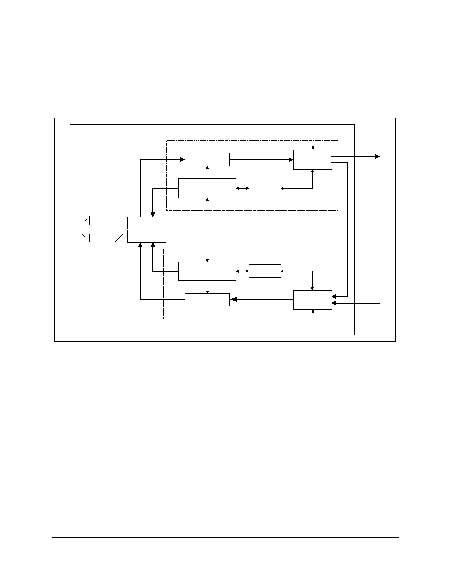
CX82100 Home Network Processor Data Sheet
7-6
Conexant Proprietary and Confidential Information
101306C
7.4
EMAC Architecture
Block diagram of the EMAC unit is shown in Figure 7-3.
Figure 7-3. EMAC Functional Block Diagram
101545_030
DMA
Interface
APB
Tx Buffer Manager
(TBM)
TXFIFO
SYNC
MAC
Transm itter
TM AC
Rx Buffer Manager
(RBM)
RXFIFO
SYNC
MAC
Receiver
RM AC
ETXD[3:0]
ERXD[3:0]
ETXCK
ERXCK
HNP
The EMAC module interfaces with the DMA controller through the DMA interface
block. The APB address is decoded in this block. Tx Buffer Manager (TBM) and Rx
Buffer Manager (RBM) blocks control the MAC Transmitter and MAC Receiver,
respectively. TBM and RBM issue the requests to the DMA controller and control their
own FIFOs.
Synchronization is required between the MAC receiver and the RBM because they
operate on different clocks (PCLK and EMx_RX_CLK, respectively). Similarly,
synchronization is required between the MAC transmitter and the TBM because they
operate on different clocks (PCLK and EMx_TX_CLK, respectively).
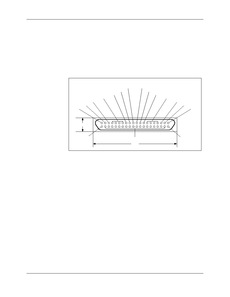
CX82100 Home Network Processor Data Sheet
101306C
Conexant Proprietary and Confidential Information
7-7
7.5
Media Independent Interface (MII)
The MII provides a port for transmit and receive data that is media independent, multi-
vendor interoperable, and supports all data rates and physical standards. The port consists
of data paths that are 4 bits wide in each direction as well as control and management
signals. Figure 7-4 shows the MII connector with signal names and the contact
assignment.
Figure 7-4. MII Connector
1015435_031
1
20
21
40
+5V
ERXD[3:0]
MDC
MDIO
ERXDV
ERXCK
ERXER
ETXER
ETXCK
ETXEN
ETXD[3:0]
ECOL
ECRS
+5V
+5V
+5V
G rounds (22-39)
50 mm
15 mm
The primary function of the MII is to provide the interface to the EPHY and necessary
digital interface for EPHY management. The MII management interface utilizes a
communications protocol similar to a serial EEPROM. The 10/100 MAC MII interface
provides all services required by the MII, including encoding and decoding of MII.

CX82100 Home Network Processor Data Sheet
7-8
Conexant Proprietary and Confidential Information
101306C
7.6
EMAC Interrupts
The EMAC provides three interrupts each for EMAC1 and EMAC2:
∑ Int_EMAC#{x}_ERR (diagnostics/exception interrupt)
∑ Int_DMAC_EMAC#{x}_RX (packet received interrupt)
∑ Int_DMAC_EMAC#{x}_TX (transmission complete interrupt)
where {x} indicates the EMAC number (1 or 2).
These interrupt bits are located in the INT_Stat register (see Section 11.2.2).
Int_EMAC#{x}_ERR is set to 1 if any number of EMAC interrupts occur. Before an
EMAC interrupt can be recognized by the HNP, its corresponding enable bit must be set
to 1 in E_IE_{x}. The equation for the Int_EMAC#{x}_ERR is as follows:
Int_EMAC#{x}_ERR =
(E_IE_AU and E_LP_AU) or
(E_IE_AI and (E_S_ES or E_S_TUF or E_S_TOF or E_S_RO or E_S_TJT or
E_S_RWT)) or
E_IE_NI and (E_LP_RI or E_LP_TI) or
(E_IE_TU and E_S_TU) or
(E_IE_RW and E_S_RWT) or
(E_IE_TOF and E_S_TOF) or
(E_IE_TUF and E_S_TUF) or
(E_IE_ED and E_S_ED) or
(E_IE_DF and E_S_DF) or
(E_IE_RLD and E_S_RLD) or
(E_IE_TF and E_S_TF) or
(E_IE_TJT and E_S_TJT) or
(E_IE_NCRS and E_S_NCRS) or
(E_IE_LCRS and E_S_LCRS) or
(E_IE_16 and E_S_16) or
(E_IE_LC and E_S_LC) or
(E_IE_RI and E_LP_RI) or
(E_IE_TI and E_LP_TI)
Int_DMAC_EMAC#{x}_RX bit field is set to 1 in the INT_Stat register after the
receiver posts the status in the status field of the RX buffer for a good packet when
E_NA_PB bit of E_NA_{x} is 0 (do not pass bad packet). When E_NA_PB is set to 1
(pass bad or good packet), The Int_DMAC_EMAC#{x}_RX bit is set after the receiver
post the status for a good or bad packet.
Int_DMAC_EMAC#{x}_TX bit field is set to 1 in the INT_Stat register after the
transmitter posts the status of the packet in the TX buffer or when the transmitter gets a
stop descriptor (ready bit in the TDES is zero).

CX82100 Home Network Processor Data Sheet
101306C
Conexant Proprietary and Confidential Information
7-9
7.7
TMAC Architecture
Before the host requests transmission of a frame, it constructs the data (LLC data) field of
the frame in memory. The TMAC appends a preamble and a SFD to the beginning of the
frame. Using information from the descriptor, TMAC also appends a PAD at the end of
the data field of sufficient length to ensure that the transmitted frame length satisfies a
minimum frame. TMAC then attempts to avoid contention with other traffic on the
medium by monitoring the carrier sense signal provided by the Ethernet PHY and
deferring to passing traffic. When the medium is clear, frame transmission is initiated
(after a brief interframe delay to provide recovery time for other devices on the medium).
The TMAC then provides data nibbles to the EPHY on the MII.
The EPHY monitors the medium and generates the collision detect signal, which, in the
contention-free case, remains off for the duration of the frame. When transmission has
completed without contention, the TMAC informs the host by writing status into the
memory and awaits the next request.
7.7.1
Transmit Frame Structure
Before the TMAC can start transmitting a frame containing the LLC data, a transmit
message structure as shown in Figure 7-5 must be constructed by the host in ARM's
memory. TMAC reads data from the memory (via DMA channel 1 or 3) to transmit via
MII and writes data into the memory to update the status. The ARM host is the master for
TMAC transmit operations and serves data to the TMAC via the APB. It is also the host's
task to assemble Ethernet frames to be sent out by the TMAC. The transmit descriptor
(TDES), the transmit status (TSTAT), and the sequence of transmitter DMA operation
are described below. Note that the qword count which is to be loaded into the
DMAC_{x}_CNT1 register should always include the first qword reserved for the
transmit status.
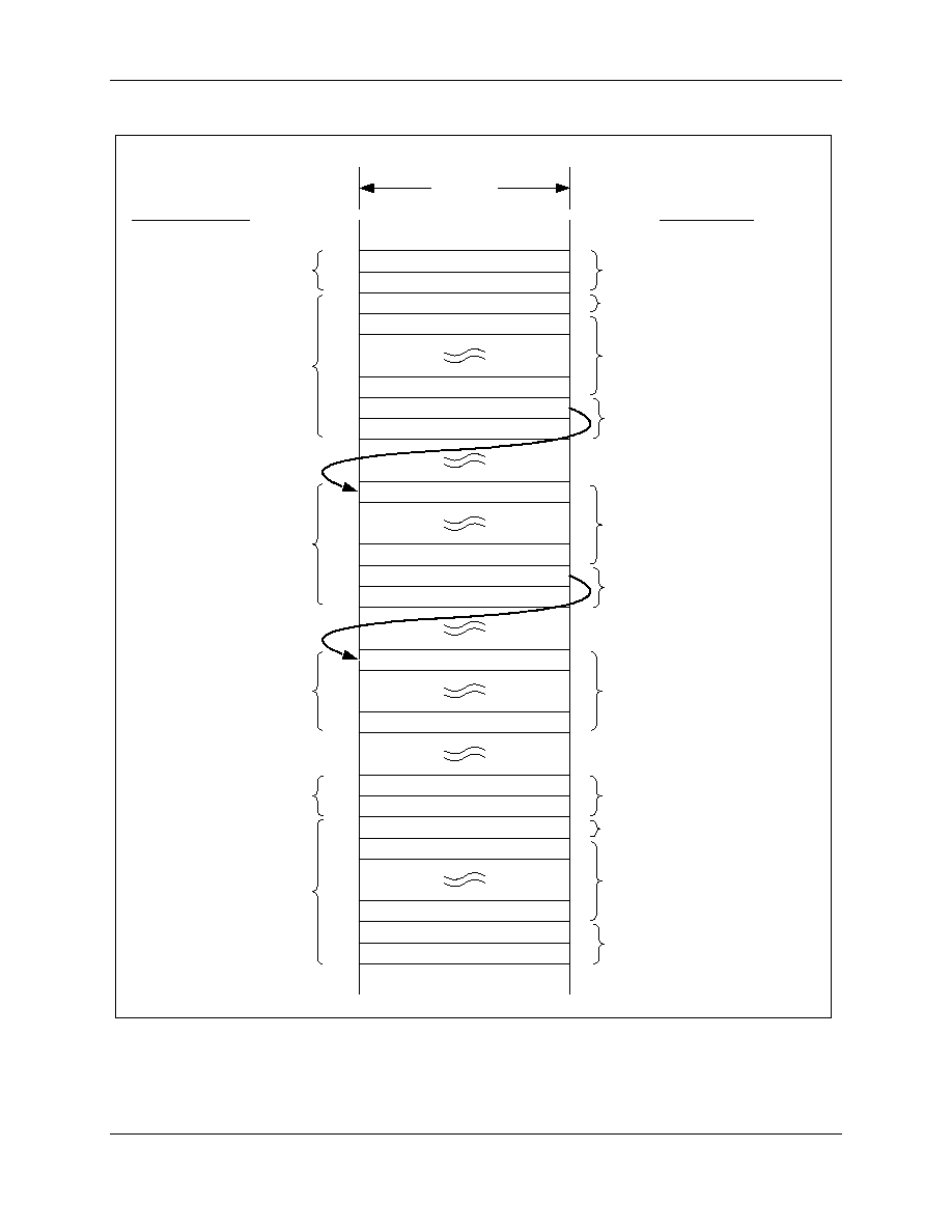
CX82100 Home Network Processor Data Sheet
7-10
Conexant Proprietary and Confidential Information
101306C
Figure 7-5. EMAC Transmit Frame Structure
101545-032
Next DMA Cnt (Frame #N)
Next DMA Ptr (Frame #N)
Data (Frame #N)
Descriptor (TDES Frame #N)
0x00000000
Status (TSTAT Frame #N)
4 Bytes
Data (Frame #N)
Next DMA Cnt (Frame #N)
Next DMA Ptr (Frame #N)
Data
N
(End of Frame #N)
Data (Frame #N)
Data (Frame #N)
Data (Frame #N)
Next DMA Cnt (Frame #N+1)
Next DMA Ptr (Frame #N+1)
Data (Frame #N+1)
Descriptor (TDES Frame #N+1)
0x00000000
Status (TSTAT Frame #N+1)
Data (Frame #N+1)
W ritten By
Used By
Requested by TMAC & Sent
to TMAC FIFO by DMAC
TM AC
ARM
ARM
ARM
TM AC
ARM
TM AC
ARM
DM AC
Requested by TMAC & Sent
to TMAC FIFO by DMAC
DM AC
Requested by TMAC & Sent
to TMAC FIFO by DMAC
Requested by TMAC & Sent
to TMAC FIFO by DMAC
TM AC
ARM
DM AC

CX82100 Home Network Processor Data Sheet
101306C
Conexant Proprietary and Confidential Information
7-11
7.7.2
Transmit Descriptor
The contents of the Transmit Descriptor (TDES) are described in Table 7-2.
Table 7-2. Transmit Descriptor Format
Bit(s)
Field
Transmit Descriptor (TDES) Description
31:17
Unused.
16
RDY
Frame Ready.
0 = Frame not ready to be transmitted.
1 = Frame ready to be transmitted.
15:4
TLEN
Transmit Frame Length.
Transmit frame length in bytes. Range is 0≠4095. This includes the preamble, SFD, DA, SA, length,
and data to transmit.
3
Reserved.
2
SET
Setup Frame.
0 = Current frame is not a setup frame.
1 = Current frame is a setup frame.
1
DPD
Disable TX Padding.
0 = Enable TX padding.
1 = Disable TX padding.
0
AC
Disable CRC Appending.
0 = Enable CRC appending.
1 = Disable CRC appending.

CX82100 Home Network Processor Data Sheet
7-12
Conexant Proprietary and Confidential Information
101306C
7.7.3
Transmit Status (TSTAT)
The contents of the Transmit Status (TSTAT) are described in Table 7-3.
Table 7-3. Transmit Status Format
Bit(s)
Default
Type
Name
Description
31
1'b0
TDN
Transmit Completed.
0 = Transmit not completed successfully.
1 = Transmit completed successfully (from buffer manager).
30
1'b0
TU
Transmit Stopped.
0 = Transmit not stopped.
1 = Transmit stopped (descriptor not ready).
29:21
Unused.
20:17
4'b0
TS
Transmit State.
0 = MII transmitter state inactive.
1 = MII transmitter state active (except during setup frames).
For test only.
16
1'b0
**
TOF
Transmit Buffer Manager FIFO Overflow.
0 = Transmit buffer manager FIFO overflow has not occurred
(MIB11).
1 = Transmit buffer manager FIFO overflow has occurred.
15
1'b0
**
TUF
Transmit Buffer Manager FIFO Underflow.
0 = Transmit buffer manager FIFO underflow has not occurred
(MIB11).
1 = Transmit buffer manager FIFO underflow has occurred (MIB11).
14
1'b0
**
ED
Excessive Transmit Deferrals.
0 = Excessive deferral did not occur.
1 = The HNP is attempting to transmit and is deferred longer than:
10 Mbps: 8192 x 400 ns
100 Mbps: 81920 x 40 ns
13
1'b0
**
DF
Frame Deferred.
0 = Frame has not been deferred at least once (MIB8).
1 = Frame has been deferred at least once (MIB8).
12
1'b0
*, **
CD
Frame Transmit Completed.
0 = Frame transmit not completed successfully (from MII interface).
1 = Frame transmit completed successfully (from MII interface).
11
1'b0
**
ES
Transmit Error Summary.
0 = Frame has not been deferred at least once (MIB8).
1 = Transmitter error summary (TF or C16 or LC or NCRS or LCRS
or TJT).
10
1'b0
**
RLD
Reload.
0 = Frame has not been deferred at least once (MIB8).
1 = Transmit FIFO reload/abort during frame (includes collisions).
9
1'b0
*, **
TF
Transmit Fault (from MII Interface).
0 = Unexpected transmit data request during frame has not
occurred.
1 = Unexpected transmit data request during frame has occurred.
8
1'b0
TJT
Transmit Jabber Timeout.
0 = Jabber timer not expired.
1 = Jabber timer expired.
E_NA_HUJ and E_NA_HUJ must be configured for this bit to function.

CX82100 Home Network Processor Data Sheet
101306C
Conexant Proprietary and Confidential Information
7-13
Bit(s)
Default
Type
Name
Description
7
1'b0
**
NCRS
No Carrier.
0 = No carrier (EMx_CRS pin never gone high) during frame
transmit.
1 = No carrier (EMx_CRS pin never transitioned high) during frame
transmit.
6
1'b0
**
LCRS
Lost Carrier.
0 = Carrier was not lost during frame transmit.
1 = Carrier was lost (EMx_CRS pin transitioned low) at least once
frame transmit (MIB18).
5
1'b0
*, **
C16
16 or More Collisions.
0 = 16 or more collisions have not occurred during frame transmit.
1 = 16 or more collisions have occurred during frame transmit.
4
1'b0
*, **
LC
Late Collision.
0 = A late collision (after the 64th byte) has not occurred during
frame transmit.
1 = A late collision (after the 64th byte) has occurred during frame
transmit (MIB16).
3:0
4'b0
**
CC
Collision Count.
Transmit collision count of the frame. Resets after the frame is
transmitted successfully (MIB9). Increments with every collision of the
current frame.
* This field resets to its default value at the start of every transmit attempt (successful or unsuccessful termination)
** This field resets to its default value after a successful transmit.
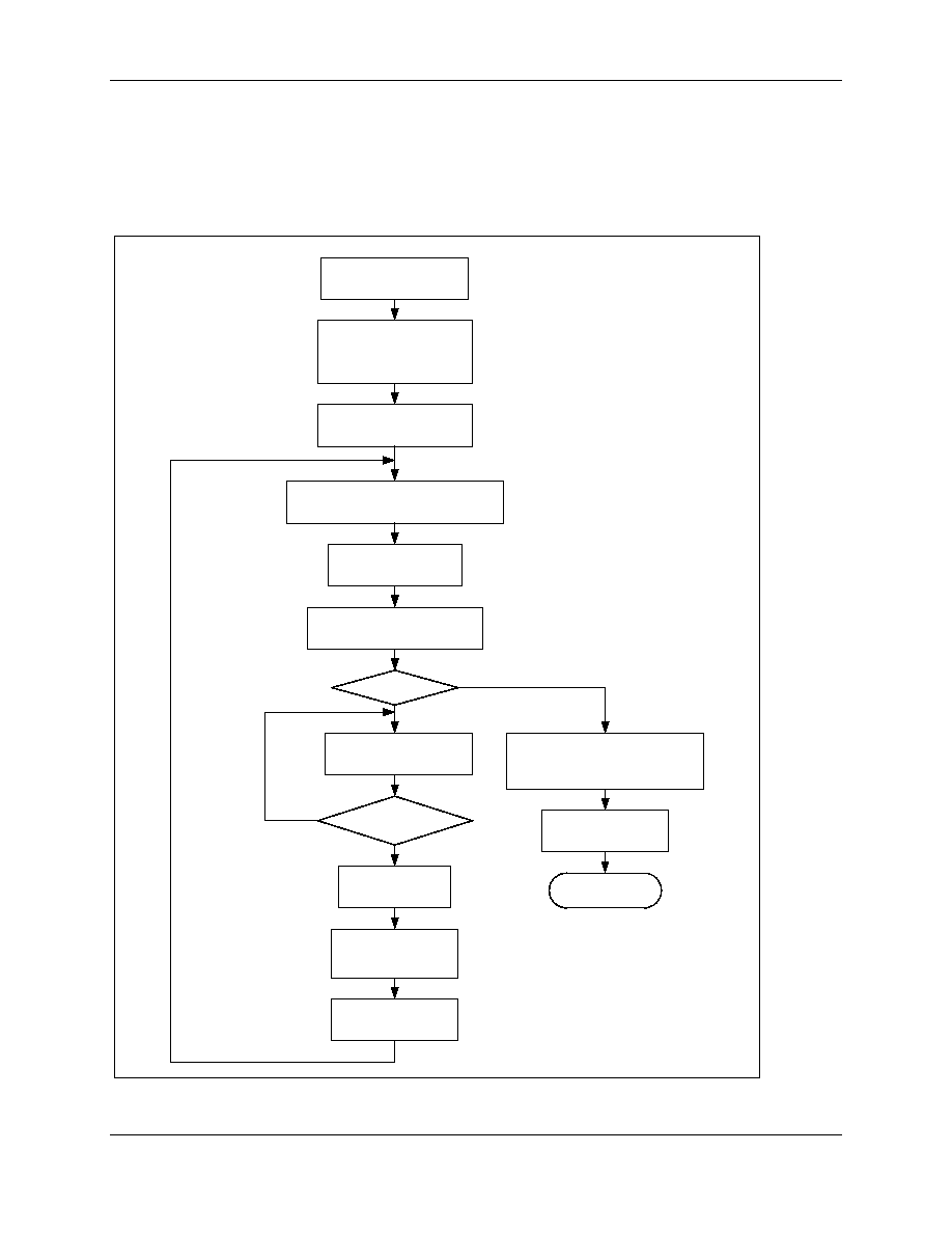
CX82100 Home Network Processor Data Sheet
7-14
Conexant Proprietary and Confidential Information
101306C
7.7.4
Sequence of Transmitter DMA Operation
TMAC DMA operation is illustrated in Figure 7-6.
Figure 7-6. TMAC DMA Operation for Channel {x} = 1 or 3
101545_033
Host programes the base
pointer DMAC_{x}_PTR1 and
the length DMAC_{x}_CNT1 for
the 1st fragment of the frame
Host assembles the frame to
be transmitted in linked list
structure and writes the TDES
Host sets the E_NA_STRT bit in
register E_NA_{x} to cause the
TMAC to start the transmission
TMAC starts the DMA on channel {x} by issuing
the DMA_SAVE command to DM AC. DMAC
saves PTR 1 to PRT2 and CNT1 to CNT2.
TMAC issues DMA_XN XT
command to DMAC to skip
the TSTAT field.
TMAC issues DMA_XNXT command
to DMAC to receive the TDES and
the 1st 4 bytes of the data.
TDES.RDY bit ON?
TM AC issues DMA_XNXT
commands to fill up the FIFO
and starts transmitting nibbles.
Last double word
received?
yes
no
no
TM AC updates the E_S_TU bit in register
E_Stat_1 (or E_Stat_2) to interrupt the
host, providing the bit E_IE_TU is set in
register E_IE_1 (or E_IE_2)
Host reads the bit
TSTAT.TDN to determine
the transmission status.
TMAC Transmission
stopped.
yes
TMAC issues
DMA_XSAVE to request
DMAC to write the TSTAT
to host memory
TMAC issues DMA_IN TR
to DMAC to signal the
end of a frame.
TMAC continues to
transmit nibbles in the
FIFO until completion.

CX82100 Home Network Processor Data Sheet
101306C
Conexant Proprietary and Confidential Information
7-15
7.8
RMAC Architecture
7.8.1
Support for the Detection of Invalid MAC Frames
As defined in the 802.3 specification, an invalid MAC frame meets at least one of the
following conditions:
∑ The frame length is inconsistent with the length field.
∑ The frame length is not an integral number of bytes.
∑ The frame bits (excluding FCS) do not generate correct CRC value (CRC mismatch).
The 802.3 specification requires that contents of invalid frames must not be passed to
LLC. This functional requirement will be handled by software. The software will be
supplied status to distinguish valid from invalid frames. This is described as follows:
Condition 1
The RMAC hardware will not parse the type/length field. In the case of a valid frame, the
hardware will infer the length based on MII signaling, and pass the length (the FL field)
as part of the "status qword" (see Section 7.8.5). For invalid frames, the length
information may or may not be available to the software. In the case where the
type/length field is type, neither hardware nor software will detect this invalid condition.
If the type/length field is length, the software will detect this condition. The type/length
field indicates whether the frame is in IEEE 802.3 format or Ethernet format. A field
greater than 1500 is interpreted as a type field, which defines the type of protocol of the
frame. A field smaller than or equal to 1500 is interpreted as a length field, which
indicates the number of data bytes in the frame.
Condition 2
The RMAC hardware will detect this invalid condition and report it in the status qword as
bit DB (dribble bit).
Condition 3
The RMAC hardware will detect and record this invalid condition by using a local
Management Information Base (MIB) counter, named "CRC" (bits 52-59 of the status
qword, see Table 7-8). This is an 8-bit counter which will be reset when the RMAC
hardware detects that a good packet has been read by the DMAC. It will be incremented
by one when a CRC mismatch occurs. This counter is passed to the software as part of
the status qword.
7.8.2
Support for the Reception Without Contention
The 802.3 specification requires that each receiving station is responsible for collecting
data bits from MII as long as the Carrier Sense signal is asserted. When Carrier Sense is
deasserted, the frame is truncated to a byte boundary, if necessary, and passed to Receive
Data Decapsulation for processing. Receive Data Decapsulation is required to check the
frame's Destination Address field to decide if the frame should be received by this
station. If so, it passes the Destination Address, the Source Address, and LLC data unit to

CX82100 Home Network Processor Data Sheet
7-16
Conexant Proprietary and Confidential Information
101306C
the LLC sublayer along with a status code indicating reception_complete or
reception_too_long (longer than 1518 bytes).
To support this requirement, address filtering (see Section 7.8.4) is to be used. Address
filtering is very computation intensive since it is required to be performed on every
packet on the Ethernet, regardless of its intended destination. Address filtering will be
supported in the RMAC hardware for "Destination Address" only. Nevertheless, the
software will be capable to program the hardware to promiscuous mode (see page 7-22),
which would pass all packets. Also, the software will be able to program the hardware to
pass bad packets. Therefore, the software will have flexibility to handle address filtering
if it so chooses.
The RMAC hardware will also provide hooks to the software to support
reception_complete or reception_too_long to allow compliance with the 802.3
specification requirement. These conditions are reported in the status qword.
7.8.3
Support for the Reception With Contention
EMx_COL asserted indicates collision detected. RMAC is required to distinguish frame
fragments received during collisions from valid frames. It will be implemented in
hardware. Early collisions will be ignored. Late collisions, after DMAC transfer
initiation, will be reported in the RMAC status qword as bit LC (late collision).
7.8.4
Address Filtering
The HNP EMAC supports address filtering in hardware for full 48-bit Ethernet
destination addresses only. The process for setting up the address filters and configuring
the filtering modes are described in the next few sections.
Setup Frame
The TMAC and RMAC operate independently during normal operation except during
setup frames. Setup frames are not transmitted on the MII interface but are looped back
from the TMAC to the RMAC and are used to program the address filters. A setup frame
defines the Ethernet addresses that are used to filter all incoming frames and must be
processed before the reception process is started, except when it operates in promiscuous
filtering mode. When processing the setup frame, the receiver logic temporarily
disengages from the MII interface and the transmission process must be running. The
setup frame is processed after all preceding frames have been transmitted and the current
frame reception (if any) is completed. The setup frame size must be exactly 192 bytes
(see Table 7-4).
Perfect Address Filtering
The HNP system can store up to 16 full 48-bit Ethernet destination addresses. RMAC
compares the destination address of any incoming frame to these addresses and decides
whether to reject or accept the frame based on the filtering mode configured in the
E_NA_1 or E_NA_2 register (defined in Section 7.11.3). This filtering method is called
perfect address filtering (as opposed to the hashing-based imperfect address filtering
defined in this section) because it accepts addresses that
∑ Do not match if in inverse filtering mode (defined in this section).
∑ Match if not in inverse filtering mode.
Table 7-4 shows the perfect address filtering Setup Frame format in the host memory.
The RMAC only keeps the column labeled "15....0" in a 48 x 16-bit hardware buffer.
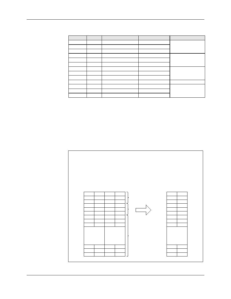
CX82100 Home Network Processor Data Sheet
101306C
Conexant Proprietary and Confidential Information
7-17
Table 7-4. Setup Frame Buffer Format
Entry No.
Bytes
Bits 31:16
Bits 15:0
Physical Address No.
0
3:0
XXXXXXXXXXXXXXXX
Bytes [1:0]
1
7:4
XXXXXXXXXXXXXXXX
Bytes [3:2]
2
11:8
XXXXXXXXXXXXXXXX
Bytes [5:4]
Address 0
3
15:12
XXXXXXXXXXXXXXXX
Bytes [1:0]
4
19:16
XXXXXXXXXXXXXXXX
Bytes [3:2]
5
23:20
XXXXXXXXXXXXXXXX
Bytes [5:4]
Address 1
6
27:24
XXXXXXXXXXXXXXXX
Bytes [1:0]
7
31:28
XXXXXXXXXXXXXXXX
Bytes [3:2]
8
35:32
XXXXXXXXXXXXXXXX
Bytes [5:4]
Address 2
. . . . .
. . . . .
. . . . .
45
183:180
XXXXXXXXXXXXXXXX
Bytes [1:0]
46
187:184
XXXXXXXXXXXXXXXX
Bytes [3:2]
47
191:188
XXXXXXXXXXXXXXXX
Bytes [5:4]
Address 15
Note that any mix of physical (i.e., unicast: the first bit of the address is 0) and logical
(i.e., multicast or group: the first bit of the address is 1) addresses can be used. Unused
addresses should be duplicated with one of the valid addresses.
Example of a Perfect Address Filtering Setup Frame
Figure 7-7 displays a perfect address filtering setup frame for two address filters.
Figure 7-7. A Perfect Address Filtering Setup Frame Buffer
101545_034
Ethernet addresses to be filtered:
(1) 25-00-26-11-27-22
(2) 09-AB-08-D1-01-15
Setup Frame in Host Buffer
(Little-Endian)
Byte No.
Setup Fram e in EM AC Buffer
(Little-Endian)
.
.
.
.
x x
x x
x x
x x
x x
x x
3
2
Byte No.
x x
x x
x x
x x
x x
x x
x x
x x
x x
x x
x x
x x
x x
x x
x x
x x
x x
x x
repeat last
valid address
A B
D 1
1 5
0 9
0 8
0 1
A B
D 1
1 5
0 9
0 8
0 1
A B
D 1
1 5
0 9
0 8
0 1
.
.
.
.
0 0
1 1
2 2
2 5
2 6
2 7
0
1
A B
D 1
1 5
0 9
0 8
0 1
A B
D 1
1 5
0 9
0 8
0 1
A B
D 1
1 5
0 9
0 8
0 1
.
.
.
.
0 0
1 1
2 2
2 5
2 6
2 7
0
1
0
47
5
4
3
2
1
6
7
8
46
45
0
47
5
4
3
2
1
6
7
8
46
45
(1)
(2)
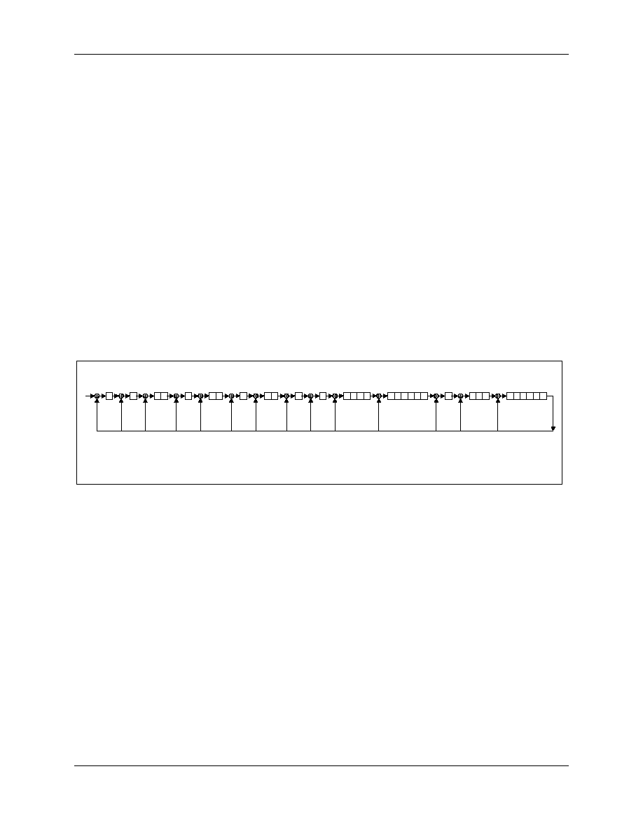
CX82100 Home Network Processor Data Sheet
7-18
Conexant Proprietary and Confidential Information
101306C
Imperfect Address Filtering
The HNP system can store 512 bits serving as hash bucket heads to support
"multicasting". The purpose of multicasting is to allow a group of nodes in a network to
receive the same message. Each node can maintain a list of multicast addresses that it will
respond to.
The multicast address filtering in the HNP system is a hardware-assisted hashing
mechanism. It can reduce the amount of CPU time required to determine whether or not
the incoming frame, with a multicast destination address, will be accepted.
For a given list of multicast addresses that the HNP system will respond to, the HNP
software first maps each multicast address into one of the 512 hash bits using the same
cyclic redundancy check (CRC) algorithm specified in the 802.3 standard. The CRC is
the 32-bit remainder of dividing a message polynomial (specified in the 802.3 standard)
by the generating polynomial G(x) =
X
32
+X
26
+X
23
+X
22
+X
16
+X
12
+X
11
+X
10
+X
8
+X
7
+X
5
+X
4
+X
2
+X+1. Figure 7-8 shows a
division circuit for G(X) using a 32-bit linear feedback shift register. The message bits
are shifted in from the left one bit at a time according to the ascending order of X in the
polynomial representation of message bits. After all bits are shifted in, the remainder is
generated and stored in the register.
Figure 7-8. A Circuit for Dividing by G(x)
101545_035
X
0
X
1
X
2
X
3
X
4
X
5
X
6
X
7
X
8
X
9
X
10
X
11
X
12
X
15
...
X
16
X
21
...
X
22
X
23
X
25
..
X
26
X
31
...
X
32
X
26
X
23
X
22
X
16
X
12
X
11
X
10
X
8
X
7
X
5
X
4
X
2
X
1
X
0
G(X) = X
32
+X
26
+X
23
+X
22
+X
16
+X
12
+X
11
+X
10
+X
8
+X
7
+X
5
+X
4
+X
2
+X+1
The same CRC algorithm will be used to map each multicast address into one of the 512
hash bits organized as a 32x16 hash table. The table is seen by the software as the lower
16 bits of the first 32 entries of the setup frame. Each 6-byte multicast address that the
node will respond to is fed into the CRC algorithm to generate a 32-bit CRC value. The
most significant 9 bits of the result is used as an index into a 32x16-bit hash table. The
upper 5 bits are used to identify the row of the table and the lower 4 bits are used to point
to the bit position of the selected row. The selected bit position will be turned on (set to
binary 1) by the software.
CX82100 Home Network Processor Data Sheet
101306C
Conexant Proprietary and Confidential Information
7-19
Table 7-5 shows the format for the setup frame involving multicast address filters. Note
that one physical address filter is included in this setup frame. This is usually the address
of the node itself.
Table 7-5. Imperfect Address Filtering Setup Frame Format
Entry No.
Bytes
Bits 31:16
Bits 15:0
0
3:0
XXXXXXXXXXXXXXXX
Hash Table Row 0
1
7:4
XXXXXXXXXXXXXXXX
Hash Table Row 1
2
11:8
XXXXXXXXXXXXXXXX
Hash Table Row 2
. . . . .
. . . . .
. . . . .
. . . . .
29
119:116
XXXXXXXXXXXXXXXX
Hash Table Row 29
30
123:120
XXXXXXXXXXXXXXXX
Hash Table Row 30
31
127:124
XXXXXXXXXXXXXXXX
Hash Table Row 31
32
131:128
XXXXXXXXXXXXXXXX
XXXXXXXXXXXXXXXX
33
135:132
XXXXXXXXXXXXXXXX
XXXXXXXXXXXXXXXX
34
139:136
XXXXXXXXXXXXXXXX
XXXXXXXXXXXXXXXX
. . . . .
. . . . .
. . . . .
39
159:156
XXXXXXXXXXXXXXXX
Physical Address (Bytes [1:0])
40
163:160
XXXXXXXXXXXXXXXX
Physical Address (Bytes [3:2])
41
167:164
XXXXXXXXXXXXXXXX
Physical Address (Bytes [5:4])
42
171:168
XXXXXXXXXXXXXXXX
XXXXXXXXXXXXXXXX
. . . . .
. . . . .
. . . . .
47
191:188
XXXXXXXXXXXXXXXX
XXXXXXXXXXXXXXXX
When a 48-bit multicast address is received, the RMAC hardware uses the same CRC
algorithm to generate the corresponding CRC value. This is shown in Figure 7-9.
The most significant 9 bits (in Little-Endian mode, these are the rightmost 9 bits of the
32-bit linear shift register) of the CRC value will be used to access a hardware hash table
that has been loaded by the setup frame described above. If the hash bit is 1 (a hit), the
frame will be accepted and delivered to the host CPU. Otherwise, the frame will be
rejected.
A hit on the hash table does not necessarily mean that the multicast frame delivered to the
host is actually destined to this node. It only assures that there is a possibility that the
incoming multicast address belongs to the node. To determine if it belongs to the node,
the host software must examine the address against the list of multicast addresses to be
accepted by this node.
This filtering method is called "imperfect" because multicast frames not addressed to this
node may slip through (an invalid address may be hashed into a bit location which is
turned on by a valid address), but it still decreases the number of frames that the host can
receive.
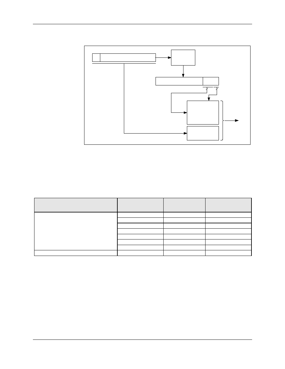
CX82100 Home Network Processor Data Sheet
7-20
Conexant Proprietary and Confidential Information
101306C
Figure 7-9. Imperfect Address Filtering
101545_036
Destination Address
IG
0
47
46
CRC Logic
Hash Table
(32x16)
32-bit CRC
0
8
9
31
0
16
one physical
address
0
31
5
4
hit/miss
if IG=0
if IG=1
Example of an Imperfect Address Filtering Setup Frame
Table 7-6 displays seven multicast addresses to be filtered imperfectly and one unicast
address to be filtered perfectly. The corresponding setup frame is displayed in Figure
7-10.
Table 7-6. Hash Index Generated Using Ethernet CRC Algorithm
Multicast/Unicast
Ethernet Address
32-Bit CRC Value in
Little-Endian Mode
Hash Index:
(Most Significant 9
Bits of the CRC Value)
0xD57701F6
0x1F6
(2) D9-C2-C0-99-0B-82
0x8C14FEBE
0x0BE
(3) E7-C1-96-36-89-DD
0x3BE71E3C
0x03C
(4) 85-00-25-00-27-00
0x4D69365E
0x05E
(5) 9D-48-4D-FD-CC-0A
0xD4BE5976
0x176
(6) C1-CC-28-55-D3-C7
0x18883CD2
0x0D2
Addresses Subject to Imperfect Filtering
(7) AB-46-0A-55-2D-7E
0x78081873
0x073
Physical Address Subject to Perfect Filtering
3A-12-C2-56-DE-91
--
--
CX82100 Home Network Processor Data Sheet
101306C
Conexant Proprietary and Confidential Information
7-21
Figure 7-10. Example of Imperfect Filtering Setup Frame
101545_037
Ethernet addresses to be filtered
Setup Fram e in Host Buffer (Little-Endian)
(1)
0
x x
x x
0 0
0 0
1
x x
x x
0 0
0 0
2
x x
x x
0 0
0 0
3
x x
x x
1 0
0 0
4
x x
x x
0 0
0 0
5
x x
x x
4 0
0 0
6
x x
x x
0 0
0 0
7
x x
x x
0 0
0 8
8
x x
x x
0 0
0 0
9
x x
x x
0 0
0 0
A
x x
x x
0 0
0 0
B
x x
x x
4 0
0 0
C
x x
x x
0 0
0 0
D
x x
x x
0 0
0 4
E
x x
x x
0 0
0 0
F
x x
x x
0 0
0 0
x x
x x
0 0
0 0
x x
x x
0 0
0 0
x x
x x
0 0
0 0
x x
x x
0 0
0 0
x x
x x
0 0
0 0
x x
x x
0 0
0 0
x x
x x
0 0
0 0
x x
x x
0 0
4 0
x x
x x
0 0
0 0
x x
x x
0 0
0 0
x x
x x
0 0
0 0
x x
x x
0 0
0 0
x x
x x
0 0
0 0
x x
x x
0 0
0 0
x x
x x
0 0
0 0
x x
x x
0 0
4 0
x x
x x
x x
x x
x x
x x
x x
x x
x x
x x
x x
x x
x x
x x
x x
x x
1 2
3 A
x x
x x
5 6
C 2
x x
x x
9 1
D E
x x
x x
x x
x x
x x
x x
x x
x x
x x
x x
x x
x x
10
11
12
13
14
15
16
17
18
19
1A
1B
1C
1D
1E
1F
20
21
22
23
24
25
26
27
28
29
2A
2B
2C
2D
2E
2F
(2)
(3)
(4)
(5)
(6)
(6)
x x
x x
x x
x x
x x
x x
x x
x x
x x
x x
x x
x x
x x
x x
x x
x x
x x
x x
x x
x x
x x
x x
x x
x x
x x
x x
3
2
0
1
Im perfect Filtering
(1) A3-C5-62-3F-25-87
(2) D9-C2-C0-99-0B-82
(3) E7-C1-96-36-89-DD
(4) 85-00-25-00-27-00
(5) 9D-48-4D-FD-CC-0A
(6) C1-CC-28-55-D3-C7
(7) AB-46-0A-55-2D-7E
Perfect Filtering
3A-12-C2-56-DE-91
Setup Frame in EMAC Buffer (Little-Endian)
0 0
0 0
0 0
0 0
0 0
0 0
1 0
0 0
0 0
0 0
4 0
0 0
0 0
0 0
0 0
0 8
0 0
0 0
0 0
0 0
0 0
0 0
4 0
0 0
0 0
0 0
0 0
0 4
0 0
0 0
0 0
0 0
0 0
0 0
0 0
0 0
0 0
0 0
0 0
0 0
0 0
0 0
0 0
0 0
0 0
0 0
0 0
4 0
0 0
0 0
0 0
0 0
0 0
0 0
0 0
0 0
0 0
0 0
0 0
0 0
0 0
0 0
0 0
4 0
1 2
3 A
5 6
C 2
9 1
D E
x x
x x
x x
x x
x x
x x
x x
x x
x x
x x
x x
x x
x x
x x
x x
x x
x x
x x
x x
x x
x x
x x
x x
x x
x x
x x
0
1
2
3
4
5
6
7
8
9
A
B
C
D
E
F
10
11
12
13
14
15
16
17
18
19
1A
1B
1C
1D
1E
1F
20
21
22
23
24
25
26
27
28
29
2A
2B
2C
2D
2E
2F
0
1
Hash
Table
Physical
Address
Byte No.
Byte No.
CX82100 Home Network Processor Data Sheet
7-22
Conexant Proprietary and Confidential Information
101306C
Address Filtering Modes
Eight different address filtering modes are supported in the HNP. These modes are
configured through the E_NA_PM, E_NA_PR, E_NA_IF, E_NA_HO, and E_NA_HP
bits of the Network Access Register (see Section 7.11.3). Table 7-7 lists the combination
of these bits to select the desired address filtering mode. Each mode is described below.
Table 7-7. Address Filtering Mode
Address Filtering Mode
E_NA_PM:
(Pass All
Multicast)
E_NA_PR:
(Receive
Any Good
Frame)
E_NA_IF:
(Inverse
Filtering)
E_NA_HO:
(Hash
Only)
E_NA_HP:
(Hash/
Perfect
Filtering)
16 Perfect Filtering
0
0
0
0
0
Inverse Filtering
0
0
1
0
0
1 Perfect Filtering +
512-Hash Bit Imperfect
Filtering
0
0
0
0
1
512-Hash Bit Imperfect
Filtering Only
0
0
0
1
1
x
1
0
0
x
Promiscuous
0
1
0
1
1
Pass All Multicast
1
0
0
1
1
Pass All Multicast + 16
Perfect Filtering
1
0
0
0
0
Pass All Multicast + 1
Perfect Filtering
1
0
0
0
1
16 Perfect Filtering Mode. RMAC provides support for the perfect filtering of up to 16
Ethernet unicast or multicast addresses. Any mix of addresses can be used. The 16
addresses used will occupy all of the allocated space in the setup-frame.
Inverse Filtering Mode. In this mode, all frames with addresses that match any of the 16
perfect addresses in the setup frame will be rejected. Frames with addresses that do not
match any of the 16 perfect addresses in the setup frame will be accepted.
One Perfect Filtering + 512-Hash Bit Imperfect Filtering Mode. RMAC supports one,
single unicast address to be perfectly filtered with an unlimited number of multicast
addresses to be imperfectly filtered. The single address that is to be perfectly filtered will
need to reside in byte locations <156, 157>, <160, 161>, <164, 165> of the setup frame.
The lower 16 bits of the first 32 entries of the setup frame is treated as a 512-bit hash
table for imperfect filtering.
This mode supports the needs of applications that require one, single physical address to
be filtered as the node's address, while allowing reception of more than 16 multicast
addresses without suffering the overhead of passing all multicast frames to the host.
512-Hash Bit Imperfect Filtering Only Mode. RMAC supports imperfect filtering for
an unlimited number of unicast addresses as well as multicast addresses. The lower 16
bits of the first 32 entries of the setup frame represents a 512-bit hash table. All addresses
are used to generate indices into the hash table. Frames with addresses causing a hash
table hit are passed.
This mode supports the needs of applications that require more than one physical address
to be filtered as the node's address, while allowing reception of more than 16 multicast
addresses without suffering the overhead of passing all multicast frames to the host.

CX82100 Home Network Processor Data Sheet
101306C
Conexant Proprietary and Confidential Information
7-23
Promiscuous Filtering Mode. RMAC supports the reception of all good frames on the
network, regardless of their destination. This mode is typically used for network
monitoring.
Pass All Multicast Filtering Mode. RMAC supports the reception of only multicast
frames.
Pass All Multicast + 16 Perfect Filtering Mode. This mode passes multicast frames and
frames with addresses matching 1 of the 16 addresses in the setup frame.
Pass All Multicast + 1 Perfect Filtering Mode. This mode passes all multicast
addresses and the single unicast address located in bytes <156, 157>, <160, 161>, <164,
165> of the setup frame.
7.8.5
Receive Status Handling
At the head of each frame received to DMAC buffering is a status qword (64 bits). Bits
59-32 of the status qword are the local MIB counters that are maintained by the hardware.
These counters (CRC, ALN, LONG, RUNT, and OFLW) can be read by the software
from the RMAC receive status as listed in Table 7-10. The MIB values are incremented,
as appropriate, for each errored packet received from the network, and inserted as part of
the status qword for each good packet that causes an interrupt when received. Each of the
local MIB counters are reset when an interrupt is generated for a good packet received.
Each of the MIB counters will maintain a value of all one's if they overflow, and a good
packet received interrupt will clear them. The contents of this status qword are shown in
Table 7-8.

CX82100 Home Network Processor Data Sheet
7-24
Conexant Proprietary and Confidential Information
101306C
Table 7-8. Definition of RMAC Receive Status
Bit(s)
Default
Name
Description
Remarks
63-60
Reserved.
59-52
0
CRC
No. of CRC Errors.
The number of errors accumulated between good frames
received. Range = 0≠255.
MIB Counter
51-48
0
ALN
No. of Alignment Errors.
The number of alignment errors accumulated between good
frames. Range = 0≠15.
MIB Counter
47-44
0
LONG
No. of Long Packets.
The number of packets >1518 bytes accumulated between
good frames. Range = 0≠15.
MIB Counter
43-36
0
RUNT
No. of Runt Packets.
The number of packets <64 bytes accumulated between good
frames. Range = 0≠255.
MIB Counter
35-32
0
OFLW
No. of Overflow Packets.
The number of packets that caused FIFO overflow
accumulated between good frames. Range = 0≠15.
MIB Counter
31-16
0
FL
Frame Length.
Frame length in bytes including CRC. Range = 0≠63.
15
0
ES
Error Summary.
0 = Error not detected.
1 = Error detected (logical OR of the following: FIFO
Overflow, CRC Error, Late Collision, Packet Too Long,
Packet Too Short).
14
0
Always 0.
13-12
0
OM
Operating Mode.
00 =
Normal operation.
01 =
Internal loopback.
10 =
External loopback.
11 =
Reserved.
11
0
TS
Packet Too Short.
0 = Packet length
64 bytes.
1 = Packet length < 64 bytes.
10
0
MF
Multicast Frame.
0 = Not multicast frame.
1 = Multicast frame.
9-8
0
Always 0.
7
0
TL
Packet Too Long.
0 = Packet length
1518 bytes.
1 = Packet length > 1518 bytes.
6
0
LC
Late Collision.
0 = Collision did not occur after DMAC transfer initiated.
1 = Collision occurred after DMAC transfer initiated.
5
0
OFT
Old Frame Type.
0 = Frame length
1500 bytes.
1 = Frame length > 1500 bytes (legacy from DIX support).
4
0
RW
Receive Watchdog.
0 = Watchdog timer expired during receipt of this packet.
1 = Watchdog timer expired during receipt of this packet.

CX82100 Home Network Processor Data Sheet
101306C
Conexant Proprietary and Confidential Information
7-25
Bit(s)
Default
Name
Description
Remarks
3
1
Always 1.
2
0
DB
Dribble Bit.
0 = Packet length is an integer multiple of 8 bits.
1 = Packet length is not an integer multiple of 8 bits.
1
0
CE
CRC Error.
0 = CRC error due to CRC mismatch not detected.
1 = CRC error due to CRC mismatch detect.
0
0
OF
FIFO Overflow.
0 = RMAC FIFO did not overflow.
1 = RMAC FIFO overflowed.
CX82100 Home Network Processor Data Sheet
7-26
Conexant Proprietary and Confidential Information
101306C
7.8.6
Sequence of Receiver DMA Operation
The sequence of receiver DMA operation is illustrated in Figure 7-11.
Figure 7-11. Sequence of Receiver DMA Operation
101545_038
Host specifies the circular buffer for
the receiving channel {x} by loading
the base pointer DMAC_{x}_Ptr1
and the length DMAC_{x}_Cnt1
Host initiates the Setup Frame to
configure the H/W address filtering.
Transmit & receive operations are
disabled.
Host controls the receive Start/Stop
by programming the E_NA_SR bit
of the E_NA_1 or E_NA_2 register
RMAC issues DMA_SAVE command to DMAC to
save DMAC_{x}_Cnt1 to DMAC_{x}_Cnt3
8 bytes of data
collected?
A Complete frame
received?
yes
no
no
yes
MIB counter are loaded to the
status double-word which is in
turn written to the head of the
received frame by DMAC.
RMAC issues DMA_XNXT to DMAC to
transfer the data to the buffer
Host programs the type of address
filtering in the E_NA_1 or E_NA_2
register (7 different types).
E_NA_SR=1?
no
yes
RMAC collects data bits from MII as
long as the Carrier Sense is aserted.
E_NA_SR deasserted?
yes
no
wait for
E_NA_SR
assertion
A good frame received?
no
RMAC Updates the
MIB counters and
aborts the frame by
sending DMA_RELD
command to DMAC
yes
RMAC interrupts the host and the
host processes the good frame
RMAC resets MIB counters and
the status double-word.
wait for
E_NA_SR
assertion

CX82100 Home Network Processor Data Sheet
101306C
Conexant Proprietary and Confidential Information
7-27
7.9
7-Wire Serial Interface (7-WS)
This mode is enabled by setting bit 7 of the EMAC x Network Access register
(E_NA_{x}). In this mode the MII interface works in serial mode and is designed to
interface to Conexant's CX24611 HomePNA 2.0 PHY/AFE or to any other GPSI
interface (AMD's "General Purpose Serial Interface," a de facto standard for MAC-to-
10Base-T device interface). All MII signals function the same way as in Ethernet mode
except that the 4-bit data is serialized on pins EMx_TXD0 and EMx_RXD0, and
EMx_TXD0 and EMx_TXEN are driven from the negative edge of EMx_TX_CLK.
Table 7-9 describes the signals for the 7-WS interface.
Table 7-9. 7-WS Interface Signals
7-WS Signal
MII Signal
Direction
Description
RXD
EMx_RXD0
Input
Receive Data.
Receive input bit stream.
RCLK
EMx_RX_CLK
Input
Receive Clock.
A 10 MHz square wave synchronized to the Receive Data and only active
while receiving an input bit stream.
RENA
EMx_RXCRS
Input
Receive Enable.
A logical input that indicates the presence of carrier on the channel.
TXD
EMx_TXD0
Output
Transmit Data.
Transmit output bit stream.
TCLK
EMx_TX_CLK
Input
Transmit Clock.
10 MHz clock.
TENA
EMx_TXEN
Output
Transmit Enable.
Transmit output bit stream enable. While asserted, it enables valid
transmit output (TXD).
CLSN
EMx_COL
Input
Collision.
A logical input that indicates that a collision is occurring on the channel.
CX82100 Home Network Processor Data Sheet
7-28
Conexant Proprietary and Confidential Information
101306C
7.10
EMAC Register Memory Map
EMAC registers are identified in Table 7-10.
Table 7-10. EMAC Registers
Register Label
Register Name
ASB Address
Type
Default Value
Ref.
E_DMA_1
EMAC 1 Source/Destination DMA Data
Register
0x00310000
RWp
(don't care)
7.11.1
E_NA_1
EMAC 1 Network Access Register
0x00310004
RW
0x80200000
7.11.3
E_Stat_1
EMAC 1 Status Register
0x00310008
RW*
0x00000000
7.11.4
E_IE_1
EMAC 1 Interrupt Enable Register
0x0031000C
RW
0x00000000
7.11.6
E_LP_1
EMAC 1 Receiver Last Packet Register
0x00310010
RW*
0x00000000
7.11.5
E_MII_1
EMAC 1 MII Management Interface Register
0x00310018
RW1
0x00000008
7.11.7
ET_DMA_1
EMAC 1 Destination DMA Data Register
0x00310020
ROp
(don't care)
7.11.2
E_DMA_2
EMAC 2 Source/Destination DMA Data
Register
0x00320000
RWp
(don't care)
7.11.1
E_NA_2
EMAC 2 Network Access Register
0x00320004
RW
0x80200000
7.11.3
E_Stat_2
EMAC 2 Status Register
0x00320008
RW*
0x00000000
7.11.4
E_IE_2
EMAC 2 Interrupt Enable Register
0x0032000C
RW
0x00000000
7.11.6
E_LP_2
EMAC 2 Receiver Last Packet Register
0x00320010
RW*
0x00000000
7.11.5
E_MII_2
EMAC 2 MII Management Interface Register
0x00320018
RW2
0x00000008
7.11.7
ET_DMA_2
EMAC 2 Destination DMA Data Register
0x00320020
ROp
(don't care)
7.11.2
Notes:
1. Bit E_MII_1[1] is read only.
2. Bit E_MII_2[1] is read only.
CX82100 Home Network Processor Data Sheet
101306C
Conexant Proprietary and Confidential Information
7-29
7.11
EMAC Registers
7.11.1
EMAC x Source/Destination DMA Data Register (E_DMA_1: 0x00310000 and
E_DMA_2: 0x00320000)
E_DMA_1 and E_DMA_2 are the EMAC source/destination DMA data registers for
EMAC1 and EMAC2, respectively (used by the EMAC DMA transmit channel).
Bit(s)
Type
Default
Name
Description
63:0
RWp
64'bx
E_DMA
A qword buffer for DMA source/destination access.
7.11.2
EMAC x Destination DMA Data Register (ET_DMA_1: 0x00310020 and
ET_DMA_2: 0x00320020)
ET_DMA_1 and ET_DMA_2 are the EMAC destination DMA data registers for EMAC1
and EMAC2, respectively (used by the EMAC DMA receive channel).
Bit(s)
Type
Default
Name
Description
63:0
ROp
64'bx
ET_DMA
A qword buffer for DMA destination access.

CX82100 Home Network Processor Data Sheet
7-30
Conexant Proprietary and Confidential Information
101306C
7.11.3
EMAC x Network Access Register (E_NA_1: 0x00310004 and E_NA_2:
0x00320004)
E_NA_1 and E_NA_2 are the EMAC Network Access registers for EMAC1 and
EMAC2, respectively.
Bit(s)
Type
Default
Name
Description
31
RW
1'b1
E_NA_RTX
TX Software Reset.
0 = No effect.
1 = Once 1 is written, write 0 into field to get out of reset. All internal
registers of RX and TX (including all bits of this register) are
reset to their default value.
30
RW
1'b0
E_NA_STOP
Stop Transmit Control.
0 = No effect.
1 = Stop the transmitter after the current frame (if any).
29:28
Unused.
27
RW
1'b0
E_NA_HP
Hash/Perfect Address Filter Mode Control.
E_NA_HP, E_NA_HO, E_NA_IF, E_NA_PR, E_NA_PM should be
programmed according to Table 7-7 to select the desired address
filtering mode.
26
RW
1'b0
E_NA_HO
Hash Only Control.
See E_NA_HP for description.
25
RW
1'b0
E_NA_IF
Inverse Filter Control.
See E_NA_HP for description.
24
RW
1'b0
E_NA_PR
Promiscuous Mode Control.
See E_NA_HP for description.
23
RW
1'b0
E_NA_PM
Pass All Multicast.
See E_NA_HP for description.
22
RW
1'b0
E_NA_PB
Pass Bad Packet Control.
0 = Disable.
1 = Receive any packets, if pass address filter, including runt
packets, CRC error, truncated packets.
21
RW
1'b1
E_NA_RRX
RX Software Reset.
0 = No effect.
1 = Once 1 is written, write 0 into field to get out of reset. All internal
RX registers are reset to their default value. This bit can only be
cleared after E_NA_RTX bit is cleared.
20
RW
1'b0
E_NA_THU
TX Test HUJ Control.
19
RW
1'b0
E_NA_DIS
TX Disable Back-Off Counter Control.
18
RW
1'b0
E_NA_RUT
TX Reset Unit Timer Control.
17:16
RW
2'b00
E_NA_IFG
Interframe Gap (IFG) Period Select.
Value is read as an integer and substitutes E_NA_IFG in the following
equations:
100 Mbps: IFG = 960 ≠ 40* E_NA_IFG ns
10 Mbps: IFG = 9600 ≠ 40* E_NA_IFG ns

CX82100 Home Network Processor Data Sheet
101306C
Conexant Proprietary and Confidential Information
7-31
Bit(s)
Type
Default
Name
Description
15
RW
1'b0
E_NA_JBD
Jabber Disable.
0 = Enable.
1 = Disable checking for exceedingly long packets during transmit
operations. If the Transmit Jabber function is enabled, E_S_TJT
will be set after the timer has expired.
E_NA_JCLK controls the duration of the Transmit Jabber Time-Out
clock.
14
RW
1'b0
E_NA_HUJ
Host Un-Jabber Control.
This field configures the time delay between a Transmit Jabber time-
out event and re-enabling the transmit process.
0 = 420 ms/42 ms.
1 = Immediate.
The bit-time is dependent on the current network operating speed.
13
RW
1'b0
E_NA_JCLK
Jabber Clock Control.
This field is used to configure the length of the timer used to detect
transmit jabber conditions and cut-off transmission.
0 = 26 ms/2.6 ms.
1 = 2560 bit-times.
12
RW
1'b0
E_NA_SB
Start/Stop Backoff Counter.
0 = Incrementing of the collision backoff counter is not stopped
while Carrier Sense is true.
1 = Incrementing of the collision backoff counter is stopped while
Carrier Sense is true. Once Carrier Sense is false, the counter
will resume incrementing.
Valid only in Half-Duplex mode. If this field is cleared, the collision
backoff counter may expire while Carrier Sense is true. Since Carrier
Sense is an indication of network activity, the HNP may attempt to
transmit and have to defer.
11
RW
1'b0
E_NA_FD
Full-Duplex Select.
0 = Configure for half-duplex operation.
1 = Configure for full-duplex operation.
10:9
RW
2'b00
E_NA_OM
Operating Mode Select.
Configures the device for normal operation or Loopback test modes.
00 = Normal operation.
10 = External Loopback test.
01 = Internal Loopback test.
11 = Reserved.
8
RW
1'b0
E_NA_FC
TX Force Collisions.
0 = Do not force collisions on each transmit attempt while in Internal
Loopback mode.
1 = Force collisions on each transmit attempt while in Internal
Loopback mode.
7
RW
1'b0
E_NA_HLAN
7-WS Enable.
0 = Enable Parallel Data Mode on MII pins.
1 = Enable 7-wire serial interface (7-WS) on MII pins.
6
RW
1'b0
E_NA_SR
Receive Start/Stop Control.
1 = Start receive.
0 = Stop receive.
5
RW
1'b0
E_NA_NS
Network Speed Select.
0 = Configure 100 Mbps network speed.
1 = Configure 10 Mbps network speed.
4
RW
1'b0
E_NA_RWR
Receive Watchdog Release Time Select.
0 = Release watchdog timer 24 bit times after carrier is deasserted.
1 = Release watchdog timer 48 bit times after carrier is deasserted.

CX82100 Home Network Processor Data Sheet
7-32
Conexant Proprietary and Confidential Information
101306C
Bit(s)
Type
Default
Name
Description
3
RW
1'b0
E_NA_RWD
Receive Watchdog Disable.
0 = If the receiving packet's length is longer than 2560 bytes, the
watchdog timer will be expired.
1 = Disable the watchdog timer.
2:1
Reserved.
0
RW
1'b0
E_NA_STRT
Start Transmit Control.
0 = No effect (this bit is self-clearing).
1 = Writing a 1 causes the transmitter to start if the transmitter was
idle and the stop bit (E_NA_STOP) is 0. E_NA_STOP (bit 30)
overrides E_NA_STRT. This bit is auto-cleared after TX is
complete whether it was successful or not.
E_NA_STRT E_NA_STOP
Description
0
0 = Do nothing
1
0 = Start transmitter
X
1 = Stop transmitter

CX82100 Home Network Processor Data Sheet
101306C
Conexant Proprietary and Confidential Information
7-33
7.11.4
EMAC x Status Register (E_Stat_1: 0x00310008 and E_Stat_2: 0x00320008)
E_Stat_1 and E_Stat_2 are the EMAC Status registers for EMAC1 and EMAC2,
respectively. Writing to this register will clear all of its bits (as denoted by RW*).
Bit(s)
Type
Default
Name
Description
31
RW*
1'b0
E_S_TU
Transmit Stopped.
0 = Descriptor ready.
1 = Descriptor not ready.
30:27
RW*
4'b0
E_S_RS
Receive State.
Indicates the receiver MII state (for test only).
26
RW*
1'b0
E_S_RO
Receive FIFO Overflow.
0 = Receive FIFO has not overflowed.
1 = Receive FIFO has overflowed.
25
RW*
1'b0
E_S_RWT
Receive Watchdog Time-Out.
0 = Receive watchdog timer has not expired.
1 = Receive watchdog timer has not expired (based on LAN_WTR).
24:21
RW*
4'b0
E_S_TDS
Transmit Buffer Manager State.
For test only.
20:17
RW*
4'b0
E_S_TS
Transmit State.
Indicates the transmitter state (except during setup frames). For test
only.
16
RW*
1'b0
E_S_TOF
Transmit FIFO Overflow.
0 = Transmit FIFO has not overflowed.
1 = Transmit FIFO has overflowed.
15
RW*
1'b0
E_S_TUF
Transmit FIFO Underflow.
0 = Transmit FIFO has not underflowed.
1 = Transmit FIFO has underflowed.
14
RW*
1'b0
E_S_ED
Excessive Transmit Deferrals.
0 = Deferred longer than 10 Mbps (8192 x 400 ns) while attempting
to transmit.
1 = Deferred longer than 100 Mbps (81920 x 40 ns) while
attempting to transmit.
13
RW*
1'b0
E_S_DF
Deferred Frame.
0 = Current transmit frame has not been deferred at least once.
1 = Current transmit frame has been deferred at least once.
12
RW*
1'b0
E_S_CD
Carrier Done.
0 = Frame transmit not done from MII interface.
1 = Frame transmit done from MII interface.
11
RW*
1'b0
E_S_ES
Transmitter Error Summary.
0 = None of the bits indicated by the 1 state are set.
1 = Any of the following transmit error status bits are set to a 1:
Transmit Fault (E_S_TF), 16+ Collisions (E_S_16), Late
Collision (E_S_LC), No Carrier (E_S_NCRS), Lost Carrier
(E_S_LCRS), or Transmit Jabber Timeout (E_S_TJT).
10
RW*
1'b0
E_S_RLD
Reload Abort.
0 = Transmit FIFO reload/abort has not occurred during current
frame (includes collisions).
1 = Transmit FIFO reload/abort has occurred during current frame
(includes collisions).

CX82100 Home Network Processor Data Sheet
7-34
Conexant Proprietary and Confidential Information
101306C
Bit(s)
Type
Default
Name
Description
9
RW*
1'b0
E_S_TF
Transmit Fault.
0 = Unexpected transmit data request has not occurred during
current frame.
1 = Unexpected transmit data request has occurred during current
frame.
8
RW*
1'b0
E_S_TJT
Transmit Jabber Timeout.
0 = Jabber timer has not expired.
1 = Jabber timer has expired.
E_NA_HUJ and E_NA_HUJ must be configured for this bit to function.
7
RW*
1'b0
E_S_NCRS
No Carrier.
0 = carrier detected.
1 = No carrier (EMx_CRS pin never transitioned high) during frame
transmit.
6
RW*
1'b0
E_S_LCRS
Lost Carrier.
0 = Carrier was not lost during frame transmit.
1 = Carrier was lost (EMx_CRS pin transitioned low) at least once
frame transmit.
5
RW*
1'b0
E_S_16
16+ Collisions.
0 = 16 or more collisions have not occurred during frame transmit.
1 = 16 or more collisions have occurred during frame transmit.
4
RW*
1'b0
E_S_LC
Late Collision.
0 = A late collision (after the 64th byte) has not occurred during
frame transmit.
1 = A late collision (after the 64th byte) has occurred during frame
transmit (MIB16).
3:0
RW*
4'b0
E_S_CC
Collision Count.
Transmit collision count of the current frame. Resets after the frame is
transmitted. Increments with every collision of the current frame.
7.11.5
EMAC x Receiver Last Packet Register (E_LP_1: 0x00310010 and E_LP_2:
0x00320010)
E_LP_1 and E_LP_2 are the EMAC Receiver Last Packet registers for EMAC1 and
EMAC2, respectively. Writing to this register will clear all of its bits (as denoted by
RW*).
Bit(s)
Type
Default
Name
Description
31:10
Reserved.
9:6
RW*
4'b0
E_LP_RDMA
Receive DMA State Machine State. (For test only.)
5:2
RW*
4'b0
E_LP_RFIFO
Receive FIFO State Machine State. (For test only.)
1
RW*
1'b0
E_LP_RI
Receive Done OK from RX Buffer Manager.
0
RW*
1'b0
E_LP_TI
Transmit Done OK from TX Buffer Manager.

CX82100 Home Network Processor Data Sheet
101306C
Conexant Proprietary and Confidential Information
7-35
7.11.6
EMAC x Interrupt Enable Register (E_IE_1: 0x0031000C and E_IE_2:
0x0032000C)
E_IE_1 and E_IE_2 are the EMAC Error Interrupt Enable registers for EMAC1 and
EMAC2, respectively.
Bit(s)
Type
Default
Name
Description
31:17
Reserved.
16
RW
1'b0
E_IE_NI
Normal Interrupt Summary Enable.
Masks E_LP_TI or E_LP_RI (1 = Enable; 0 = Disable).
15
RW
1'b0
E_IE_RW
Receive Watchdog Timer Interrupt Enable.
Masks E_S_RWT (1 = Enable; 0 = Disable).
14
RW
1'b0
E_IE_RI
Receive OK Interrupt Enable.
Masks E_LP_RI (1 = Enable; 0 = Disable).
13
RW
1'b0
E_IE_AI
Abnormal Interrupt Summary Enable.
Masks E_S_ES or E_S_TUF or E_S_TOF or E_S_RO or E_S_TJT or
E_S_RWT (1 = Enable; 0 = Disable).
12
RW
1'b0
E_IE_LC
Late Collision Interrupt Enable.
Masks E_S_LC (1 = Enable; 0 = Disable).
11
RW
1'b0
E_IE_16
16 Collisions Interrupt Enable.
Masks E_S_16 (1 = Enable; 0 = Disable).
10
RW
1'b0
E_IE_LCRS
Lost Carrier Interrupt Enable.
Masks E_S_LCRS (1 = Enable; 0 = Disable).
9
RW
1'b0
E_IE_NCRS
No Carrier Interrupt Enable.
Masks E_S_NCRS (1 = Enable; 0 = Disable).
8
RW
1'b0
E_IE_TF
Transmit Fault Interrupt Enable.
Masks E_S_TF (1 = Enable; 0 = Disable).
7
RW
1'b0
E_IE_RLD
Transmit Reload/Abort Interrupt Enable.
Masks E_S_RLD (1 = Enable; 0 = Disable).
6
RW
1'b0
E_IE_ED
Excessive Deferral Interrupt Enable.
Masks E_S_ED (1 = Enable; 0 = Disable).
5
RW
1'b0
E_IE_DF
Transmit Deferred Interrupt Enable.
Masks E_S_DF (1 = Enable; 0 = Disable).
4
RW
1'b0
E_IE_TOF
Transmit Overflow Interrupt Enable.
Masks E_S_TOF (1 = Enable; 0 = Disable).
3
RW
1'b0
E_IE_TUF
Transmit Underflow Interrupt Enable.
Masks E_S_TUF (1 = Enable; 0 = Disable).
2
RW
1'b0
E_IE_TJT
Transmit Jabber Time-out Interrupt Enable.
Masks E_S_TJT (1 = Enable; 0 = Disable).
1
RW
1'b0
E_IE_TU
Transmit Stopped Interrupt Enable.
Masks E_S_TU (1 = Enable; 0 = Disable).
0
RW
1'b0
E_IE_TI
Transmit OK Interrupt Enable.
Masks E_LP_TI (1 = Enable; 0 = Disable).

CX82100 Home Network Processor Data Sheet
7-36
Conexant Proprietary and Confidential Information
101306C
7.11.7
EMAC x MII Management Interface Register (E_MII_1: 0x00310018 and E_MII_2:
0x00320018)
E_MII_1 and E_MII_2 are the EMAC MII Management Interface registers for EMAC1
and EMAC2, respectively.
Bit(s)
Type
Default
Name
Description
31:5
Reserved.
4
RW
1'b0
E_MDIP
Active Edge of EMx_MDC Pin in Input Mode.
0 = EMx_MDIO is sampled on the falling edge of EMx_MDC.
1 = EMx_MDIO is sampled on the rising edge of EMx_MDC.
3
RW
1'b1
E_MM
Direction of Signal on EMx_MDIO Pin.
0 = EMx_MDIO pin is an output.
1 = EMx_MDIO pin is an input.
2
RW
1'b0
E_MDO
Value Driven on EMx_MDIO Pin.
0 = Drive EMx_MDIO pin low when E_MM = 0 (output mode).
1 = Drive EMx_MDIO pin high when E_MM = 0 (output mode).
1
RO
1'b0
E_MDI
Value Read on EMx_MDIO Pin.
0 = EMx_MDIO pin is low when E_MM = 1 (input mode).
1 = EMx_MDIO pin is high when E_MM = 1 (input mode).
0
RW
1'b0
E_MDC
Value Driven on EMx_MDC Pin.
0 = Drive EMx_MDC pin low.
1 = Drive EMx_MDC pin high.

CX82100 Home Network Processor Data Sheet
101306C
Conexant Proprietary and Confidential Information
8-1
8
USB Interface Description
The USB Interface (or UDC Core) consists of three major functions: USB Controller
(USBC), APB/DMA Interface (I/F), and USB Differential Transceiver (Figure 8-1). The
USBC includes the following functions:
∑ Phase Locked Loop (PLL) Block. The PLL Block extracts the USB clock and data
from the USB cable. The input to the PLL Block comes from an USB Differential
Transceiver. The PLL runs on a 48 MHz clock. The PLL also generates a 12 MHz
clock from the 48 MHz clock and supplies it to the Serial Interface Engine (SIE) and
USB Bridge Layer (UBL) blocks. The PLL identifies the Single Ended Zero (SE0)
signal on the USB and sends it to the SIE Block.
∑ Serial Interface Engine (SIE) Block. The SIE Block performs the front end
functions of the USB protocol such as SyncField identification, NRZI-NRZ
conversion, token packet decoding, bit stripping, bit stuffing, NRZ-NRZI
conversion, CRC5 checking, and CRC16 generation and checking. The SIE also
converts the serial packet to 8-bit parallel data. The SIE Block has a 1-byte buffer for
buffering the data during data transmission and reception.
∑ USB Bridge Layer (UBL) Block. The UBL Block handles the error recovery
mechanism during transactions while interfacing to the Application (the Application
includes the APB/DMA I/F, the ARM940T Processor, and the ARM firmware
processing the data). The UBL also decodes and handles all the Standard Control
Transfers addressed to Endpoint Zero. The UBL passes some USB commands onto
the APB/DMA I/F so that the Application can decode and process the command. The
UBL Block has two sub-blocks called the Protocol Layer (PL) Block and the
Endpoint (EP) Block.
The PL Block controls the SIE Block by providing necessary handshake signals to
the SIE and communicates with the APB/DMA I/F. It also performs error recovery if
the APB/DMA I/F violates the data transfer protocol.
The EP Block handles all the Control transfers to Endpoint Zero. The EP Block
decodes and responds to all the USB Standard Commands and some other USB
Commands (e.g., Get Descriptor) to the APB/DMA I/F. The EP Block maintains the
buffer for Device Address, buffer for storing the present active Configuration, and
the logic to determine the present state of the Device (USBC).
∑ Endpoint Information (EPINFO) Block: The EPINFO maintains the registers that
store information about the endpoints. The EPINFO also stores the information about
the size of Configuration in the USBC. The information about the current endpoint is
multiplexed from these registers and is provided to the PL Block which controls the
SIE Block based on this information. The EPINFO also includes the
DATA0/DATA1 synchronization bits for each bidirectional endpoint the USBC
supports. Also, the EPINFO includes the EndPtStalled bit for each of the supported
logical endpoints to indicate the Stalled Status of the Endpoint. The HNP EPINFO
supports up to 3 active bidirectional logical endpoints and one interrupt endpoint.
The endpoint number ranges from 0 to 4.
CX82100 Home Network Processor Data Sheet
8-2
Conexant Proprietary and Confidential Information
101306C
Figure 8-1. Block Diagram of the USB Interface
101545_054
Protocol
Layer
(PL)
Block
Endpoint
(EP)
Block
Endpoint
Inform ation
(EPINFO)
Block
USB Bridge Layer
(UBL) Block
Transm itter
Receiver
Serial Interface
(SIE) Block
SYNC
PLL
USB
Differential
Transceiver
USB Controller (USBC)
USB
APB/DMA
Interface
(I/F)
APB
USB Interface (UDC Core)
HNP
CX82100 Home Network Processor Data Sheet
101306C
Conexant Proprietary and Confidential Information
8-3
8.1
UDC Data Path
The UDC data path supports USB transmit and receive data.
8.1.1
USB Transmit Data Path (Endpoint IN Channel)
The USB transmit data flow is illustrated in Figure 8-2.
Figure 8-2. USB Transmit Data Flow
101545_055
Data
Buffer
UBL
from APB/
DMA I/F
HandShake
Generator
Data +
CRC16
M
U
X
Token
Assembly
Bit
Stuffing
NRZ-to-NRZI
Conversion
to USB
Differential
Transceiver
CRC16
data
payload
ACK,
NAK,
ST ALL
IN,
OUT ,
SOF,
SETUP
complete
packet
0
1
0
1
0
1
1
1
1
0
1
1
1
1
1
bit
stuffing
NRZ
NRZI
+
-
NRZ
to
NRZI
conversion
0 = inverting the polarity of the output signal
1 = not inverting the output signal
CX82100 Home Network Processor Data Sheet
8-4
Conexant Proprietary and Confidential Information
101306C
8.1.2
USB Receive Data Path (Endpoint OUT Channel)
The USB receive data flow is illustrated in Figure 8-3.
Figure 8-3. USB Receive Data Flow
101545_056
Data
Buffer
UBL
to APB/
DMA I/F
Address
Checker
Data/CRC
Checker
NRZI-to-
NRZ
Conversion
Sync Field
Indentification
PLL
from USB
DIfferential
Transceiver
PID
Decode
Handshake
Checker
Serial-to-
Parallel
Conversion
0
0
0
0
0
0
0
1
NRZI
data
PI
D
0
PI
D
2
PI
D
1
SYNC Pattern

CX82100 Home Network Processor Data Sheet
101306C
Conexant Proprietary and Confidential Information
8-5
8.2
USB Data Flow
USB data can be identified as control, bulk, or interrupt data in the HNP.
Control data is usually structured as a command phase initiated by the USB host,
followed by data either provided by the device (IN), i.e., HNP (IN), or sent to it by the
host (OUT), followed in turn by a status phase which serves as an acknowledgement of
transfer. Control transfers are directed to Endpoint 0, and requires no device
configuration, i.e., control transfers can be active from the moment of device attachment.
All other transfers require device configuration and setting of the appropriate device
address by the host to be accepted by the HNP. In another words, a process called
enumeration is must be initiated by the host every time the HNP is connected. Control
data flow through Endpoint 0 must be USB Specification Rev. 1.1 Chapter 9 compliant
and other USB stack command aware. Packet size for Endpoint 0 is 64 bytes for control
data and 8 bytes for control command.
Bulk transfers are simple data transfers with ACK/NAK token exchange between the host
and the HNP to signal the completion of the transfer. Again, these transfers are started by
the host sending a IN (OUT) token to the HNP, which responds within a timeout period
with data and/or ACK/NAK (depending on the direction of transfer) to keep the host
from retrying to transfer the data. The packet size for bulk transfers is always less than or
equal to 64 bytes.
Interrupt data is infrequent data that flows only from the HNP to the host and is a result
of the host polling the HNP periodically. The HNP Interrupt Endpoint is fixed at IN type
with 8 bytes per packet.

CX82100 Home Network Processor Data Sheet
8-6
Conexant Proprietary and Confidential Information
101306C
8.3
UDC Core
The USB Core includes the endpoint buffers and associated processing.
8.3.1
Endpoint Buffer Format
The UDC stores all the endpoint configuration information for each endpoint that the
HNP supports. Each endpoint configuration is stored in a separate Buffer called
EndPtBuf. The UDC Core has defined the logical and physical endpoints for its
implementation. A "logical endpoint" is an endpoint that is visible to the host. Generally,
for USB, there are 16 logical endpoints from the host's perspective (Endpoint 0 to
Endpoint 15). At any time the host can access one of these logical endpoints. A "physical
endpoint", on the other hand, is the actual unidirectional endpoint that is implemented in
the hardware. Two physical endpoints can be paired to form a bidirectional endpoint
sharing the same logical endpoint number.
The UDC supports one configuration, one interface, no alternate interface, three
bidirectional endpoints plus one interrupt endpoint (seven physical endpoints total). Since
each endpoint requires 5 bytes for its endpoint configuration, then the total number of
endpoint configuration bytes allocated within the UDC Core are (5 * 7) + 5 (Endpoint 0).
Firmware initializes these EndPtBuf Configuration bytes upon POR or Hardware Reset
event. Please refer to Section 8.3.3 for the procedure to initialize these Endpoint Buffer
Configurations.
Table 8-1. Endpoint Buffer Format in UDC Core
Bit(s)
Type
Description
39:36
EP_NUM
Logical Endpoint Number.
35:34
EP_CONFIG
Configuration Number.
Only configuration 1 is supported.
33:32
EP_INTERFACE
Interface Number.
Three interfaces (0, 1, or 2) are supported.
31:29
EP_ALTSETTING
Alternate Setting.
Only alternate setting 0 for each interface is
supported.
28:27
EP_TYPE
Type of Endpoint.
00 = Control.
01 = Isochronous.
10 = Bulk.
11 = Interrupt.
26
EP_DIR
Direction of Data Flow.
0 = Out.
1 = In.
This bit is ignored for control endpoints.
25:16
EP_MAXPKTSIZE
Maximum Packet Size for this Endpoint.
15:0
EP_BUFADRPTR
Address Pointer for the Associated Endpoint.
Only bits [3:0] are used.
This must match with the pointer specified in
U_CTR2 register for transfer to take place. It is
always zero for Endpoint 0.
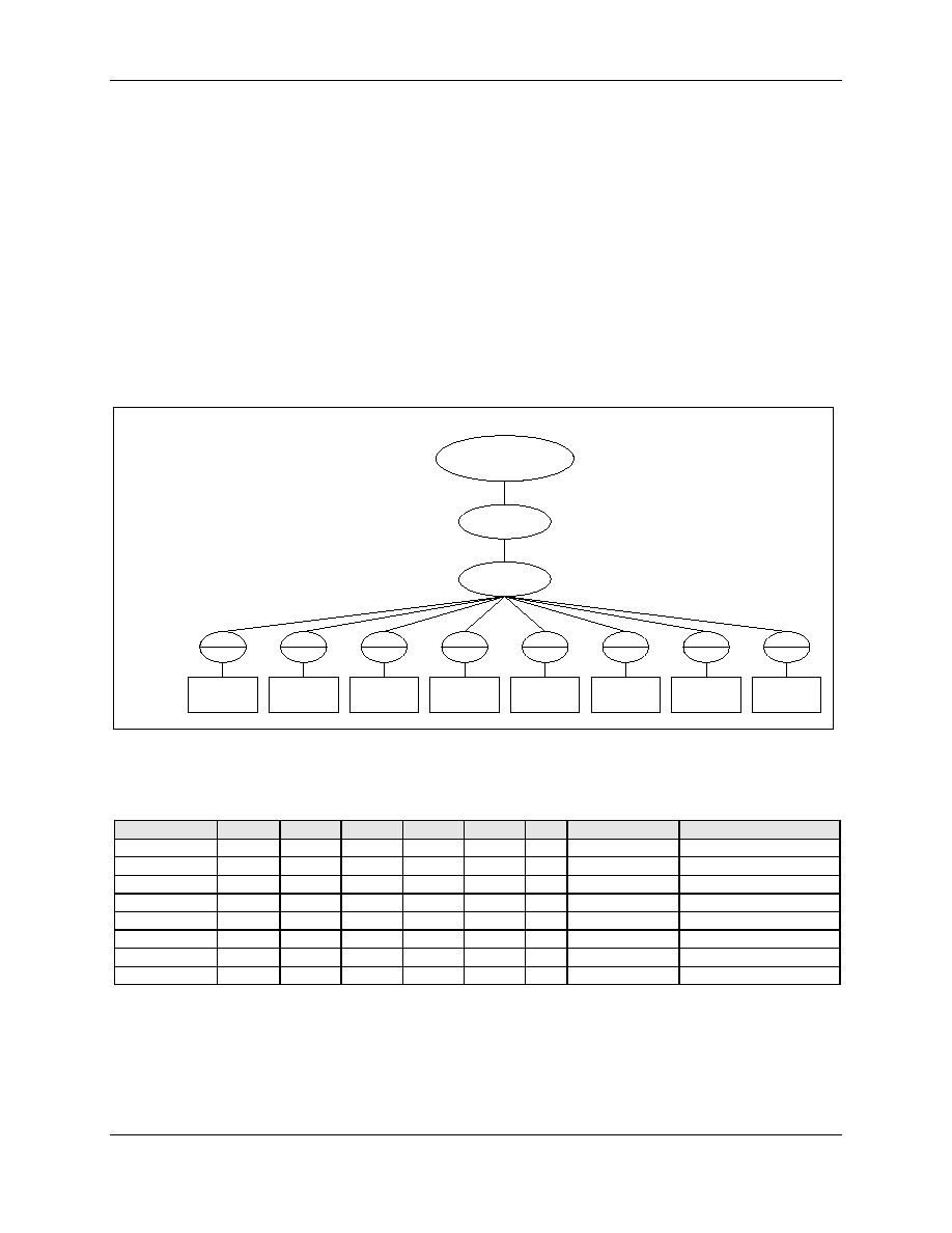
CX82100 Home Network Processor Data Sheet
101306C
Conexant Proprietary and Confidential Information
8-7
8.3.2
Example of Endpoint Buffer Encoding
As shown in Figure 8-4, the HNP supports one configuration, one interface with no
alternate setting and four logical endpoints (Endpoints 1, 2, 3, and 4). The first three
endpoints are bidirectional endpoints and the fourth is an interrupt endpoint, therefore
there are nine physical endpoints total (including controlled Endpoint 0). In the UDC, one
EndPtBuf (Endpoint Buffer) is associated with each physical endpoint. Hence, there are
eight EndPtBufs in the UDC for the configuration shown in Figure 8-4. Endpoint 0 needs
only one EndPtBuf, although it is bidirectional.
An example of the encoding of the EndPtBuf is shown in Table 8-2. Except for interrupt
endpoint's packet size being fixed at 8 bytes, other endpoints' packet size must be less
than or equal to 64 bytes.
Figure 8-4. Example of an USB Device for HNP
101545_057
Configuration 1
Interface 0
Alt Setting 0
Logical No.
Physical No.
EP 0
1
Control
EP 1
2
Bulk-IN
EP 1
3
Bulk-OUT
EP 2
4
Bulk-IN
EP 2
5
Bulk-OUT
EP 3
6
Bulk-IN
EP 3
7
Bulk-OUT
EP 4
8
Interrupt
Table 8-2. Example of the EndPtBuf Encoding
EndPtBuf No.
39:36
35:34
33:32
31:29
28:27
26
25:16
15:0
1
0000
01
00
000
00
0
00 0100 0000
0000 0000 0000 0000
2
0001
01
00
000
10
0
00 0100 0000
0000 0000 0000 0001
3
0001
01
00
000
10
1
00 0100 0000
0000 0000 0000 0001
4
0010
01
00
000
10
0
00 0100 0000
0000 0000 0000 0001
5
0010
01
00
000
10
1
00 0100 0000
0000 0000 0000 0010
6
0011
01
00
000
10
0
00 0100 0000
0000 0000 0000 0011
7
0011
01
00
000
10
1
00 0100 0000
0000 0000 0000 0011
8
0100
01
00
000
11
1
00 0001 0100
0000 0000 0000 0100

CX82100 Home Network Processor Data Sheet
8-8
Conexant Proprietary and Confidential Information
101306C
8.3.3
Loading of the EndPtBuf Configurations
The endpoint configuration in the UDC Core is accomplished by writing to the U_CFG
register the same byte-wise data that the UDC Core expects. The target of these
configuration writes are the endpoint buffers which have the format shown in Table 8-1.
Starting from the Endpoint 0 descriptor (EndPtBuf0), the configuration data is written to
EndPtBuf0[39:32], followed by EndPtBuf0[31:24], and so on (EndPtBuf0 is reserved for
Endpoint 0). Once the 5-byte EndPtBuf0 has been filled, EndPtBuf1, and the others are
filled in order, most significant byte first. Since the register writes from APB are 4 bytes
in length, the data is grouped so that the first byte to the UDC interface comes from the
least significant byte of the register U_CFG. After the contents of the register write have
been passed on to the UDC Core, the firmware is requested, via the CFGNEXT_INT flag
in the U_STAT register, to write the next 4 bytes of configuration data. This continues
until the endpoint descriptors have been updated, with the assertion of CFGDN_INT
status. During configuration, the CFG_EN control bit is set to prevent any data from
being transferred to erroneous addresses. Once the configuration data has been loaded,
the CFG_EN bit is reset and endpoints are enabled through the setting of their enable bits
in the U_CTR1 register. Prior to enabling the endpoints, the endpoint addresses in the
U_CTR2 register must be programmed to match those passed to the endpoint descriptors
EP_BUFADRPTR parameters in the EndPtBuf.
USB GLOBAL EN bit (bit0 of U_CTR1) can only set once per POR or Hardware Reset
event, after that the UDC Core will accept the endpoint configuration data as described in
the sequences above. USB RESET bit (Bit 30 of U_CTR1) can be used to reset the UDC
Core the same way as POR or a Hardware Reset event.
Figure 8-5 shows the example of loading the EndPtBuf configurations described in Table
8-2.
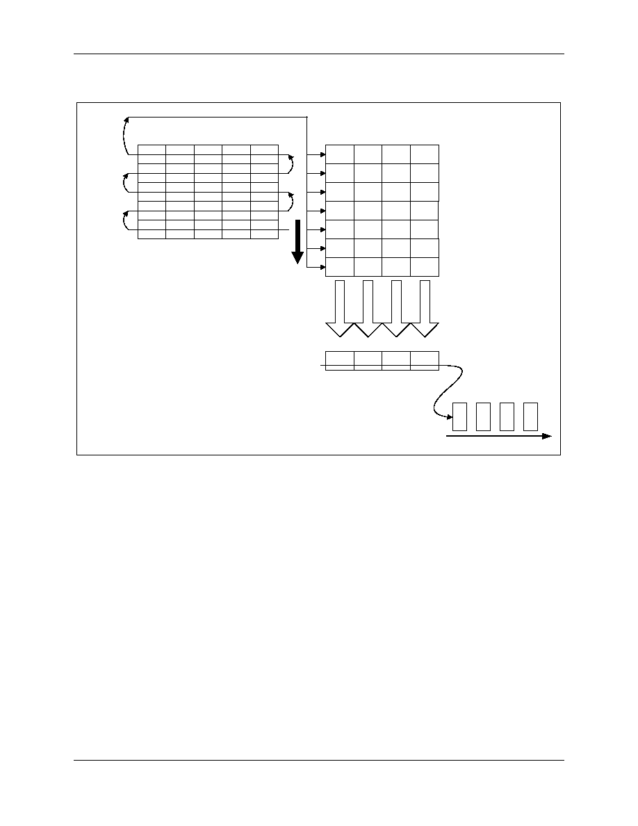
CX82100 Home Network Processor Data Sheet
101306C
Conexant Proprietary and Confidential Information
8-9
Figure 8-5. Loading of the EndPtBuf Configurations
B#7
B#6
B#5
B#4
B#3
B#2
B#1
B#0
B#14
B#13
B#12
B#11
B#10
B#9
B#8
B#39
B#38
B#37
B#36
....
....
....
B#35
....
....
B#3
B#2
B#1
B#0
101545_058
39:32
31:24
7:0
15:8
23:16
EndPtBuf0
EndPtBuf1
EndPtBuf4
EndPtBuf3
EndPtBuf2
U_CFG
Register
31:24
7:0
15:8
23:16
APB By
t
e
La
ne
0
APB By
t
e
La
ne
3
APB By
t
e
La
ne
2
APB By
t
e
La
ne
1
B#
0
B#
3
B#
2
B#
1
To USB Interface Block
B#7
B#6
B#5
B#4
B#3
B#2
B#1
B#0
B#15
B#14
B#13
B#12
B#11
B#10
B#9
B#8
B#19
B#18
B#17
B#16
B#39
B#38
B#37
B#36
....
....
....
....
8.3.4
USB Command Handling
The UDC handles and decodes all USB Standard Commands defined in the USB
Specification Rev. 1.1. The UDC returns a STALL HandShake if it receives an
unsupported or invalid Standard Command. The UDC will forward all controlled
commands (Endpoint 0), as well as other Endpoint OUT Data, to the application via a
DMA RX buffer except the following controlled commands which are decoded
internally:
∑ Clear Feature
∑ Get Configuration
∑ Get Interface
∑ Get Status
∑ Set Address
∑ Set Configuration
∑ Set Feature
∑ Set Interface
CX82100 Home Network Processor Data Sheet
8-10
Conexant Proprietary and Confidential Information
101306C
8.4
USB DMA Interface
DMAC interfaces with the USB device through addressed writes/reads that conform to
the common DMA protocol.
8.4.1
DMA Receive Channel
The DMA channel supporting receive OUT endpoints is illustrated in Figure 8-6. The
endpoint data is described in Table 8-3.
Figure 8-6. DMA Channel Supporting USB Receive OUT Endpoints
101545_059
ARM Host
DM AC
USB Device
DMA Ch 12
DMA Ch 12
EP0_OUT
Endpoints
EP3_OUT
EP2_OUT
EP1_OUT
Table 8-3. DMA Channel Supporting USB Receive OUT Endpoints
Endpoint
No.
Direction
Name
DMA
Channel
Description
Endpoint 0
OUT
EP0_OUT
12
USB specification Chapter 9 compliance
and other USB stack aware commands.
Maximum packet size is 64 bytes.
Endpoint 1
OUT
EP1_OUT
12
Bulk OUT data. Maximum packet size is
64 bytes.
Endpoint 2
OUT
EP2_OUT
12
Bulk OUT data. Maximum packet size is
64 bytes.
Endpoint 3
OUT
EP3_OUT
12
Bulk OUT data. Maximum packet size is
64 bytes.
Whenever the host sends a control/data packet that is forwarded by the HNP, the data is
then organized in 8-byte qword segments by the UDC Core and written to a circular
DMA RX buffer (the pointer and buffer length has been initialized for DMA Channel 12
operation by the firmware). Each forwarded packet consists of an 8-byte Status Header
followed by packet control/data payload arranged in little endian byte order. The exact
number of bytes of the received data/control packet is specified in the COUNT parameter
of the Status Header. In case of a transaction having a non-integer of qword boundary,
the last qword in the USB RX buffer segment holding that packet's data is zero-padded in
higher order locations. Firmware also keeps track of the next packet pointer location in
the circular DMA RX buffer. The Status Header is defined in Table 8-4.

CX82100 Home Network Processor Data Sheet
101306C
Conexant Proprietary and Confidential Information
8-11
Table 8-4. Status qword for Receive (OUT) Endpoint APB Buffers
Bit(s)
Default
Name
Description
63:16
0
Reserved.
15
0
PKT_IN
Packet has been received without errors.
14:12
0
Reserved.
11:8
0
EP_NUM
Endpoint address pointer that received this packet.
7
0
SETUP
Current packet is a setup packet.
6:0
0
COUNT
Count of data bytes received in this packet.
After the DMA Channel 12 pointer and counter (circular RX DMA Buffer) and
EP_OUT_RX_BUFSIZE register are initialized, the RV_INIT bit in U_CTR1 register is
set and cleared (in the next instruction) before enabling endpoint OUT operation. This bit
is not set again until new RX DMA buffer setting is required and only when all receive
endpoints have been disabled. Data transfer from the host to the HNP commences if there
is space in the RX DMA buffer, and continues until the RX DMA buffer is full.
Requests to DMAC are generated whenever there is data in the RX FIFO of a given
endpoint, and USB ACK has not been received. Upon reception of USB ACK, data is
flushed into the RX DMA buffer, a qword Status Header is written to the beginning of
the buffer, and the EP_OUT_RX_PEND register is increased by one. Simultaneously, a
status bit (EP0O_INT, EP1O_INT, EP2O_INT, or EP3O_INT) is set in the U_STAT
register confirming the successful reception of data on that endpoint. A RX DMA
interrupt request is forwarded to the interrupt controller if the interrupt is enabled and
also if trigger conditions are satisfied. Interrupt events can be set from a variety of
interrupt sources: Single Packet Completion, Multiple Packet Completion, and/or Packet
Pending receive watchdog timeout.
The firmware parses the endpoint information from the Status Header and acts
accordingly. When any number of RX packets are safely processed by firmware, then the
same number is written to the EP_OUT_RX_DEC register so the UDC Core can reuse
the packets' DMA buffers. There will be no new packets transferred to the RX DMA
buffer if EP_OUT_RX_PEND = EP_OUT_RX_BUFSIZE which also triggers an RX
DMA Overrun condition.
The USB RX DMA logic always initializes the next DMA Status Header packet with 0
after the first RX packet is received from the host. This can cause a problem if RX DMA
overrun condition happens (RX DMA buffer full with all 64 bytes packet size) due to
firmware overhead and system latency. Thus, it may be necessary to increase the
hardware buffer size by 8 bytes so that the most recent unprocessed Status Header
content is still intact if when overrun does occur. Note that DMAC Channel 12 count
register should be limited to 16376 bytes due to restriction of DMAC count register.
Since the maximum hardware RX DMA buffer for each data packet is 72 bytes (64 bytes
of data and 8 bytes of Status Header). With a given DMA RX buffer size in bytes, the
value programmed into the following registers should be:
DMAC_12_Cnt1 = (DMA RX buffer size) / 8
EP_OUT_RX_BUFSIZE = ((DMA RX buffer size) / 72) - 1
CX82100 Home Network Processor Data Sheet
8-12
Conexant Proprietary and Confidential Information
101306C
8.4.2
DMA Transmit Channel
The DMA channels supporting USB transmit IN endpoints are illustrated in Figure 8-6.
The endpoint data is described in Table 8-3.
Figure 8-7. DMA Channels for USB Transmit IN Endpoints
101545_060
ARM Host
DMAC
Endpoints
USB Device
EP0_IN (Ch 13)
EP1_IN (Ch 11)
EP3_IN (Ch 9)
EP2_IN (Ch 10)
DMA Ch 10
DMA Ch 11
DMA Ch 13
DMA Ch 9
DMA Ch 10
DMA Ch 11
DMA Ch 13
DMA Ch 9
Table 8-5. DMA Channels for USB Transmit IN Endpoints
Endpoint
No.
Direction
Name
DMA
Channel
Description
Endpoint 0
IN
EP0_IN
13
Control data. Maximum packet size is 64
bytes.
Endpoint 1
IN
EP1_IN
11
Bulk IN data. Maximum packet size is 64
bytes.
Endpoint 2
IN
EP2_IN
10
Bulk IN data. Maximum packet size is 64
bytes.
Endpoint 3
IN
EP3_IN
9
Bulk IN data. Maximum packet size is 64
bytes.
The firmware sets up all four IN endpoint (Endpoint0 ≠ Endpoint3) TX DMA embedded
link-list circular buffers associated with DMAC DMA channels separately. The
APB/DMA I/F then obtains and sends endpoint data from these linked-list buffers to the
UDC Core in response to host requests. Each individual TX DMA packet buffer consists
of a qword Descriptor + Status header followed by 64 bytes of data payload and qword
embedded link-list pointer/counter pointed to next packet buffer.
After setting up the proper DMA buffer associated with particular endpoint and resetting
the proper EPX_IN_DMA_RESET bit in U_CTR1 register, the firmware activates the
endpoint, optionally enables endpoint interrupt, and is then ready for data transfer.
Once an endpoint data is ready, the firmware puts proper endpoint description (Table 8-6)
and data payload (up to 64 bytes) into corresponding the TX DMA packet buffer at the
current DMA pointer.
CX82100 Home Network Processor Data Sheet
101306C
Conexant Proprietary and Confidential Information
8-13
The descriptor also contains the count of bytes to be sent in the current packet and the
logical endpoint address corresponding to that endpoint. If there is a mismatch between
the endpoint address from the buffer descriptor and the corresponding endpoint descriptor
in UDC Core, the "invalid header" status bit EPXI_INVLDHDR_INT is set and transfer
is aborted. Similar action happens if the count of bytes in the current packet is more than
64.
The firmware maintains a DMA pointer of current TX DMA packet buffer for each
endpoint. Firmware then updates the EPX_IN_TX_INC register with the number of
added data packets. APB/DMA I/F logic then transfers the data out from TX DMA buffer
into the endpoint TX FIFO buffer.
When the USB host sends a request for either bulk data or control data, then UDC
responds with the data from the TX FIFO if it has anything to transmit and continues
fetching data from TX DMA buffer if needed, or sends a NAK if data is unavailable.
When data is available, upon receiving an ACK, the status (Table 8-7) is updated with
XMIT_DONE bit and the requested logical EP_NUM number, also EPX_IN_TX_PEND
register is updated and reflecting current pending packets. The corresponding endpoint
interrupt is triggered, if enabled, and if all conditions are satisfied. If the transfer is
NAKed or an error happens during transmission, the current packet data for that endpoint
is resent.
On each consecutive NAKs from USB host, the endpoint retry counter is increased by
one. After a number of unsuccessful retries (the number programmed in the
EPXI_ERRCNT bits in U_CTR3 register), an error status bit EPXI_ERRCNT_INT is set
in the U_STAT register.
Table 8-6. Descriptor qword for Transmit (IN) Endpoint TX DMA Packet Buffer
Bit(s)
Default
Name
Description
63:16
0
Reserved.
15
0
RDY
Buffer is ready with the entire packet to be transmitted.
14:12
0
Reserved.
11:8
0
EP_NUM
Endpoint address pointer this packet transmits on.
7
0
Reserved.
6:0
0
COUNT
Count of data bytes to be transmitted in this packet.
Table 8-7. Status qword for Transmit (IN) Endpoint TX DMA Packet Buffer
Bit(s)
Default
Name
Description
63:24
0
Reserved.
23
0
XMT_DONE
Transmission of data from current buffer complete.
22:20
0
Reserved.
19:16
0
EP_NUM
Endpoint address pointer this packet transmits on.
15:0
0
Reserved.

CX82100 Home Network Processor Data Sheet
8-14
Conexant Proprietary and Confidential Information
101306C
8.5
Interrupt Endpoint
The interrupt endpoint is different from the other endpoints in that it does not get its data
from the TX DMA buffers or there is no TX DMA channel available for interrupt
endpoint. The interrupt endpoint relies on firmware writes to the U_IDAT register for the
interrupt data. Two writes to U_IDAT are required to furnish the 8 bytes of data for each
interrupt packet. After the first 4 bytes have been processed, a status bit
INTRNEXT_INT in U_STAT is set to indicate that the firmware can now write the next
4 bytes to U_IDAT. An INTRDN_INT status is set upon completion of the data transfer
to the host.
8.6
Summary of the Endpoints
The UDC Endpoints are summarized in Table 8-8.
Table 8-8. UDC Endpoints
UDC Logical Endpoint No.
UDC Physical Endpoint No.
Direction
Transfer Type
Endpoint 0
1
IN
Control
Endpoint 0
2
OUT
Control
Endpoint 1
3
IN
Bulk
Endpoint 1
4
OUT
Bulk
Endpoint 2
5
IN
Bulk
Endpoint 2
6
OUT
Bulk
Endpoint 3
7
IN
Bulk
Endpoint 3
8
OUT
Bulk
Endpoint 4
9
IN
Interrupt

CX82100 Home Network Processor Data Sheet
101306C
Conexant Proprietary and Confidential Information
8-15
8.7
USB Register Memory Map
USB registers are identified in Table 8-9.
Table 8-9. USB Registers
Register Label
Register Name
ASB Address
Type
Default
Value
Ref.
U0_DMA
USB Source/Destination DMA Data
Register 0
0x00330000
RWp
(don't care)
8.8.1
U1_DMA
USB Source/Destination DMA Data
Register 1
0x00330008
RWp
(don't care)
8.8.2
U2_DMA
USB Source/Destination DMA Data
Register 2
0x00330010
RWp
(don't care)
8.8.3
U3_DMA
USB Source/Destination DMA Data
Register 3
0x00330018
RWp
(don't care)
8.8.4
UT_DMA
USB Destination DMA Data Register
0x00330020
RO
(don't care)
8.8.5
U_CFG
USB Configuration Data Register
0x00330024
RW
0x00000000
8.8.6
U_IDAT
USB Interrupt Data Register
0x00330028
RW
0x00000000
8.8.7
U_CTR1
USB Control Register 1
0x0033002C
RW
0x04000000
8.8.8
U_CTR2
USB Control Register 2
0x00330030
RW
0x00000000
8.8.9
U_CTR3
USB Control Register 3
0x00330034
RW
0x00000000
8.8.10
U_STAT
USB Status
0x00330038
RR
0x00000000
8.8.11
U_IER
USB Interrupt Enable Register
0x0033003C
RW
0x00000000
8.8.12
U_STAT2
USB Status Register 2
0x00330040
RR
0x00000000
8.8.13
U_IER2
USB Interrupt Enable Register 2
0x00330044
RW
0x00000000
8.8.14
EP0_IN_TX_INC
EP0_IN Transmit Increment Register
0x00330048
RW
0x00000000
8.9.1
EP0_IN_TX_PEND
EP0_IN Transmit Pending Register
0x0033004C
RO
0x00000000
8.9.2
EP0_IN_TX_QWCNT
EP0_IN Transmit qword Count Register
0x00330050
RO
0x00000000
8.9.3
EP1_IN_TX_INC
EP1_IN Transmit Increment Register
0x00330054
RW
0x00000000
8.9.4
EP1_IN_TX_PEND
EP1_IN Transmit Pending Register
0x00330058
RO
0x00000000
8.9.5
EP1_IN_TX_QWCNT
EP1_IN Transmit qword Count Register
0x0033005C
RO
0x00000000
8.9.6
EP2_IN_TX_INC
EP2_IN Transmit Increment Register
0x00330060
RW
0x00000000
8.9.7
EP2_IN_TX_PEND
EP2_IN Transmit Pending Register
0x00330064
RO
0x00000000
8.9.8
EP2_IN_TX_QWCNT
EP2_IN Transmit qword Count Register
0x00330068
RO
0x00000000
8.9.9
EP3_IN_TX_INC
EP3_IN Transmit Increment Register
0x0033006C
RW
0x00000000
8.9.10
EP3_IN_TX_PEND
EP3_IN Transmit Pending Register
0x00330070
RO
0x00000000
8.9.11
EP3_IN_TX_QWCNT
EP3_IN Transmit qword Count Register
0x00330074
RO
0x00000000
8.9.12
EP_OUT_RX_DEC
EP_OUT Receive Decrement Register
0x00330078
RW
0x00000000
8.9.13
EP_OUT_RX_PEND
EP_OUT Receive Pending Register
0x0033007C
RO
0x00000000
8.9.14
EP_OUT_RX_QWCNT
EP_OUT Receive qword Count Register
0x00330080
RO
0x00000000
8.9.16
EP_OUT_RX_BUFSIZE
EP_OUT Receive Buffer Size Register
0x00330084
RW
0x00000000
8.9.15
U_CSR
USB Control-Status Register
0x00330088
RO/WO
0x00000000
8.9.20
UDC_TSR
UDC Time Stamp Register
0x0033008C
RO
0x00000000
8.8.15
UDC_STAT
UDC Status Register
0x00330090
RO
0x00000000
8.8.16
USB_RXTIMER
USB Receive DMA Watchdog Timer
Register
0x00330094
RW
0x00000000
8.9.17
USB_RXTIMERCNT
USB Receive DMA Watchdog Timer
Counter Register
0x00330098
RO
0x00000000
8.9.18
EP_OUT_RX_PENDLEVEL
EP_OUT Receive Pending Interrupt
Level Register
0x0033009C
RW
0x00000000
8.9.19
CX82100 Home Network Processor Data Sheet
8-16
Conexant Proprietary and Confidential Information
101306C
8.8
USB Registers
8.8.1
USB Source/Destination DMA Data Register 0 (U0_DMA: 0x00330000)
U0_DMA is the USB source/destination DMA data register (used by DMA Transmit
Channel 13 hardware for USB Endpoint 0 IN channel). Not used by firmware.
Bit(s)
Type
Default
Name
Description
63:0
RWp
64'bx
U0_DMA
A qword buffer for USB DMA source/destination access.
8.8.2
USB Source/Destination DMA Data Register 1 (U1_DMA: 0x00330008)
U1_DMA is the USB source/destination DMA data register (used by DMA Transmit
Channel #11 hardware for USB Endpoint 1 IN channel). Not used by firmware.
Bit(s)
Type
Default
Name
Description
63:0
RWp
64'bx
U1_DMA
A qword buffer for USB DMA source/destination access.
8.8.3
USB Source/Destination DMA Data Register 2 (U2_DMA: 0x00330010)
U2_DMA is the USB source/destination DMA data register (used by DMA Transmit
Channel #10 hardware for USB Endpoint 2 IN channel). Not used by firmware.
Bit(s)
Type
Default
Name
Description
63:0
RWp
64'bx
U2_DMA
A qword buffer for USB DMA source/destination access.
8.8.4
USB Source/Destination DMA Data Register 3 (U3_DMA: 0x00330018)
U3_DMA is the USB source/destination DMA data register (used by DMA Transmit
Channel #9 hardware for USB Endpoint 3 IN channel). Not used by firmware.
Bit(s)
Type
Default
Name
Description
63:0
RWp
64'bx
U3_DMA
A qword buffer for USB DMA source/destination access.

CX82100 Home Network Processor Data Sheet
101306C
Conexant Proprietary and Confidential Information
8-17
8.8.5
USB Destination DMA Data Register (UT_DMA: 0x00330020)
UT_DMA is the USB destination DMA data register (used by the USB DMA Receive
hardware Channel #12). Not used by firmware.
Bit(s)
Type
Default
Name
Description
63:0
RO
64'bx
UT_DMA
A qword buffer for USB DMA destination access.
8.8.6
USB Configuration Data Register (U_CFG: 0x00330024)
U_CFG is the USB configuration data register.
Bit(s)
Type
Default
Name
Description
31:0
RW
32'b0
U_CFG
UDC Configuration Data Transfer. Requires successive 4-byte
writes with handshaking control until all the configuration data has
been transferred and the CFGDNINT status bit is set.
8.8.7
USB Interrupt Data Register (U_IDAT: 0x00330028)
U_IDAT is the interrupt data register.
Bit(s)
Type
Default
Name
Description
31:0
RW
32'b0
U_IDAT
USB Interrupt Channel Data Transfer. Requires two successive
writes with handshaking control for each 8-byte interrupt data packet.

CX82100 Home Network Processor Data Sheet
8-18
Conexant Proprietary and Confidential Information
101306C
8.8.8
USB Control Register 1 (U_CTR1: 0x0033002C)
Bit(s)
Type
Default
Name
Description
31
RW
1'b0
USB_IE
Global USB Interrupt Enable.
0 = Disable all USB related interrupts.
1 = Enable all USB related interrupts enabled. Each individual
interrupt can be further controlled by its corresponding
interrupt enable bit.
30
RW
1'b1
USB_RESET
USB Reset.
Writing a 1 will reset the entire USB device (including the UDC
Core) to default state. Software must clear this bit by writing a 0 or
reading it. This bit self-clears after being read.
29
RW
1'b0
AI_RESUME
Application Initiated Resume.
This is an application initiated Resume signal. Writing a 1 to this bit
will resume the USB bus from the Suspended Mode. The peripheral
must assert the Dev_Resume signal to the UDC Core for one 12
MHz clock period. Setting this bit is meaningful only when the USB
bus is in the Suspended mode.
In response to this signal, the UDC will deassert the UDC_Suspend
signal, drive the non-IDLE (K State) onto the USB Cable for 12 ms,
and perform the Remote Wakeup Operation. When the
UDC_Suspend signal is deasserted in response to the assertion of
the Dev_Resume signal, the peripheral must restart the clock (to
the UDC Core) as soon as possible in order for the Core to start the
counters for counting the Wakeup sequence time.
This bit self-clears one cycle after it is been set.
28
RW
1'b0
RV_INIT
Buffer Pointer Initialized Flag.
Set by firmware before activating OUT Endpoints, but after writing
the pointer to the circular RX DMA buffer. Must be reset by firmware
at the next instruction.
27:16
RW
13'b0
Reserved. Should be written to all 0s.
15
RW
1'b0
EP3_IN_DMA_RESET
Endpoint 3 IN DMA Channel Reset.
Writing a 1 to this bit resets the DMA channel associated with the
EP3_IN endpoint. Must be reset to a 0 by firmware and can be done
immediately after setting to a 1.
14
RW
1'b0
EP2_IN_DMA_RESET
Endpoint 2 IN DMA Channel Reset.
Writing a 1 to this bit resets the DMA channel associated with the
EP2_IN endpoint. Must be reset to a 0 by firmware and can be done
immediately after setting to a 1.
13
RW
1'b0
EP1_IN_DMA_RESET
Endpoint 1 IN DMA Channel Reset.
Writing a 1 to this bit resets the DMA channel associated with the
EP1_IN endpoint. Must be reset to a 0 by firmware and can be done
immediately after setting to a 1.

CX82100 Home Network Processor Data Sheet
101306C
Conexant Proprietary and Confidential Information
8-19
Bit(s)
Type
Default
Name
Description
12
RW
1'b0
EP0_IN_DMA_RESET
Endpoint 0 IN DMA Channel Reset.
Writing a 1 to this bit resets the DMA channel associated with the
EP0_IN endpoint. Must be reset to a 0 by firmware and can be done
immediately after setting to a 1.
11
RW
1'b0
XVER_SLEEP
USB Transceiver Sleep Mode Select.
0 = Do not power down the USB transceiver active.
1 = Power down the USB transceiver.
10
RW
1'b0
INTR_EN
Interrupt Endpoint Enable.
0 = Disable Interrupt Endpoint.
1 = Enable Interrupt Endpoint.
9
RW
1'b0
EP3I_EN
Endpoint 3 IN Enable.
0 = Disable Endpoint 3 IN.
1 = Enable Endpoint 3 IN.
8
RW
1'b0
EP2I_EN
Endpoint 2 IN Enable.
0 = Disable Endpoint 2 IN.
1 = Enable Endpoint 2 IN.
7
RW
1'b0
EP1I_EN
Endpoint 1 IN Enable.
0 = Disable Endpoint 1 IN.
1 = Enable Endpoint 1 IN.
6
RW
1'b0
EP0I_EN
Endpoint 0 IN Enable.
0 = Disable Endpoint 0 IN.
1 = Enable Endpoint 0 IN.
5
RW
1'b0
EP3O_EN
Endpoint 3 OUT Enable.
0 = Disable Endpoint 3 OUT.
1 = Enable Endpoint 3 OUT.
4
RW
1'b0
EP2O_EN
Endpoint 2 OUT Enable.
0 = Disable Endpoint 2 OUT.
1 = Enable Endpoint 2 OUT.
3
RW
1'b0
EP1O_EN
Endpoint 1 OUT Enable.
0 = Disable Endpoint 1 OUT.
1 = Enable Endpoint 1 OUT.
2
RW
1'b0
EP0O_EN
Endpoint 0 OUT Enable.
0 = Disable Endpoint 0 OUT.
1 = Enable Endpoint 0 OUT.
1
RW
1'b0
CFG_EN
UDC Configuration Mode Enable.
0 = Disable UDC Configuration Mode.
1 = Enable UDC Configuration Mode.
0
RW
1'b0
USB_EN
USB Enable.
0 = Disable USB.
1 = Enable USB.
Never disable once enabled or the endpoints will not work!
CX82100 Home Network Processor Data Sheet
8-20
Conexant Proprietary and Confidential Information
101306C
8.8.9
USB Control Register 2 (U_CTR2: 0x00330030)
Bit(s)
Type
Default
Name
Description
27:24
RW
4'b0
INTR_ADDR
Endpoint 4 IN Address.
23:20
RW
4'b0
EP3I_ADDR
Endpoint 3 IN Address.
19:16
RW
4'b0
EP2I_ADDR
Endpoint 2 IN Address.
15:12
RW
4'b0
EP1I_ADDR
Endpoint 1 IN Address.
11:8
RW
4'b0
EP3O_ADDR
Endpoint 3 OUT Address.
7:4
RW
4'b0
EP2O_ADDR
Endpoint 2 OUT Address.
3:0
RW
4'b0
EP1O_ADDR
Endpoint 1 OUT Address.

CX82100 Home Network Processor Data Sheet
101306C
Conexant Proprietary and Confidential Information
8-21
8.8.10
USB Control Register 3 (U_CTR3: 0x00330034)
Bit(s)
Type
Default
Name
Description
29
RW
1'b0
EP3O_STALL_EN
Endpoint 3 OUT Stall Control.
Reset by the hardware when Endpoint 3 OUT has been stalled.
28
RW
1'b0
EP2O_STALL_EN
Endpoint 2 OUT Stall Control.
Reset by the hardware when the endpoint has been stalled.
27
RW
1'b0
EP1O_STALL_EN
Endpoint 1 OUT Stall Control.
Reset by the hardware when the endpoint has been stalled.
26
RW
1'b0
EP0O_STALL_EN
Endpoint 0 OUT Stall Control.
Reset by the hardware when the endpoint has been stalled.
25
RW
1'b0
EP3I_STALL_EN
Endpoint 3 IN Stall Control.
Reset by the hardware when the endpoint has been stalled.
24
RW
1'b0
EP2I_STALL_EN
Endpoint 2 IN Stall Control.
Reset by the hardware when the endpoint has been stalled.
23
RW
1'b0
EP1I_STALL_EN
Endpoint 1 IN Stall Control.
Reset by the hardware when the endpoint has been stalled.
22
RW
1'b0
EP0I_STALL_EN
Endpoint 0 IN Stall Control.
Reset by the hardware when the endpoint has been stalled.
21
RW
1'b0
INTR_STALL_EN
Interrupt Endpoint Stall Control.
Reset by the hardware when the endpoint has been stalled.
20
RW
1'b0
RST_INTR_ERRCNT
Reset for Interrupt Endpoint Retries Count.
(NAK count register)
19
RW
1'b0
RST_EP3I_ERRCNT
Reset for Endpoint 3 IN Retries Count.
(NAK count register)
18
RW
1'b0
RST_EP2I_ERRCNT
Reset for Endpoint 2 IN Retries Count.
(NAK count register)
17
RW
1'b0
RST_EP1I_ERRCNT
Reset for Endpoint 1 IN Retries Count.
(NAK count register)
16
RW
1'b0
RST_EP0I_ERRCNT
Reset for Endpoint 0 IN Retries Count.
(NAK count register)
15
1'b0
Reserved.
14:12
RW
3'b0
INTR_ERRCNT
Interrupt Endpoint Retries Count.
11:9
RW
3'b0
EP3I_ERRCNT
Endpoint 3 IN Retries Count.
(NAK count)
8:6
RW
3'b0
EP2I_ERRCNT
Endpoint 2 IN Retries Count.
(NAK count)
5:3
RW
3'b0
EP1I_ERRCNT
Endpoint 1 IN Retries Count.
(NAK count)
2:0
RW
3'b0
EP0I_ERRCNT
Endpoint 0 IN Retries Count.
(NAK count)

CX82100 Home Network Processor Data Sheet
8-22
Conexant Proprietary and Confidential Information
101306C
8.8.11
USB Status (U_STAT: 0x00330038)
If an interrupt status bit in this register is set by the UDC, the USB Interrupt bit in the
Interrupt Status Register (INT_Stat) is set if the corresponding enable bit in the U_IER
register is set. Writing a 1 to a bit location will clear the interrupt status bit; writing a 0
has no effect.
Bit(s)
Type
Default
Name
Description
28
RR
1'b0
RX_PEND_NONZERO_INT
Receive Pending Register Nonzero Interrupt.
0 = Receive pending register is zero.
1 = Receive pending register is nonzero.
27
RR
1'b0
UDC_LatchIntfVal_INT
UDC_LatchIntfVal Interrupt.
0 = UDC_LatchIntfVal signal is not asserted.
1 = UDC_LatchIntfVal signal is asserted.
The UDC_LatchIntfVal signal is asserted by the UDC Core for
one clock, when the core receives a valid Set-Interface SETUP
command to a supported Interface and supported Alternate
Interface Setting. The signal is asserted when the UDC issues
an ACK handshake to the SETUP transfer of the Set-Interface
Command. The Interface to which this command is addressed
is available on the UDC_InterfaceVal[1:0] and the value of the
new Alternate Setting is available on the UDC_AltIntfVal[2:0]
outputs.
Using the UDC_LatchIntfVal signal, the Application can know
the Set-Interface Command along with the Interface Number to
which it is addressed to and the Alternate Setting Value,
without doing a full decode of the Setup transfer. Applications
supporting Dynamic Alternate Interfaces, can use this signal to
identify the new Alternate Setting of the Interface being
selected.
26
RR
1'b0
UDC_LatchCfgVal_INT
UDC_LatchCfgVal Interrupt.
0 = UDC_LatchCfgVal signal is not asserted.
1 = UDC_LatchCfgVal signal is asserted.
The UDC_LatchCfgVal signal is asserted by the UDC Core for
one clock, when the core receives a valid Set-Configuration
SETUP command to a supported configuration. The signal is
asserted when the UDC issues an ACK handshake to the
SETUP transfer of the Set-Configuration Command. The Value
of the new configuration is available on the
UDC_ConfigVal[1:0] outputs.
Using the UDC_LatchCfgVal signal, the Application can know
the Set-Configuration Command and the Configuration value
with out doing a full decode of the Setup transfer. Applications
supporting Dynamic Configurations or applications that do
power management based on the Current Configuration, can
use this signal to identify the new Configuration the Device is
being selected.

CX82100 Home Network Processor Data Sheet
101306C
Conexant Proprietary and Confidential Information
8-23
Bit(s)
Type
Default
Name
Description
25
RR
1'b0
UDC_UsbReset_INT
UDC_UsbReset Interrupt.
0 = UDC_UsbReset signal is not asserted.
1 = UDC_UsbReset signal is asserted.
The UDC_UsbReset signal is asserted by the UDC Core
whenever the core observes more than 2.5 us (32 FS bit
times/4 LS bit times) of SE0 on the D+/D- lines. Once
asserted, UDC_UsbReset is kept asserted as long as the SE0
is observed on the D+/D- lines.
24
RR
1'b0
UDC_Sof_INT
UDC_Sof Interrupt.
0 = UDC_Sof signal is not asserted.
1 = UDC_Sof signal is asserted.
The UDC_Sof signal is asserted by the UDC Core for one
clock every time an entire SOF Packet is successfully decoded
on the USB.
The UDC_Sof signal is at logic `0' when Reset and when
asserted will be at logic `1'.
23
RR
1'b0
USB_SUSPEND_INT
USB Suspend Detected Interrupt.
0 = USB Cable not in Suspend Mode.
1 = USB Cable in Suspend Mode. UDC has detected that
the USB Cable is in the Suspended Mode i.e., the USB
is idle for 3 ms. The Device should go into SUSPEND
mode whenever this bit is on and should meet all the
USB Specification Requirements for the Suspend Mode.
It is the responsibility of the peripheral to stop the Clock
so that min. power is consumed when the Device is in
Suspended Mode.
22
RR
1'b0
USB_RESUME_INT
USB Resume Detected Interrupt.
0 = USB Cable not in Resume Mode.
1 = USB Cable in Resume Mode. UDC has detected a non-
IDLE (K State) on the USB Cable while the USB cable
is in Suspended Mode.
21
RR
1'b0
EP3I_INVLDHDR_INT
Endpoint 3 IN Invalid Header Interrupt.
0 = Invalid header not detected.
1 = Invalid header detected for Endpoint 3 IN channel buffer
list.
20
RR
1'b0
EP2I_INVLDHDR_INT
Endpoint 2 IN Invalid Header Interrupt.
0 = Invalid header not detected.
1 = Invalid header detected for Endpoint 2 IN channel buffer
list.
19
RR
1'b0
EP1I_INVLDHDR_INT
Endpoint 1 IN Invalid Header Interrupt.
0 = Invalid header not detected.
1 = Invalid header detected for Endpoint 1 IN channel buffer
list.
18
RR
1'b0
EP0I_INVLDHDR_INT
Endpoint 0 IN Invalid Header Interrupt.
0 = Invalid header not detected.
1 = Invalid header detected for Endpoint 0 IN channel buffer
list.
17
RR
1'b0
INTR_NAK_INT
Interrupt Channel NAKed on Current Transfer.
16
RR
1'b0
INTR_ERRCNT_INT
Interrupt Channel Exceeded Max Retries Count.

CX82100 Home Network Processor Data Sheet
8-24
Conexant Proprietary and Confidential Information
101306C
Bit(s)
Type
Default
Name
Description
15
RR
1'b0
EP3I_ERRCNT_INT
Endpoint 3 IN Error Count Interrupt.
0 = Endpoint 3 IN retries count not exceeded.
1 = Endpoint 3 IN retries count exceeded.
14
RR
1'b0
EP2I_ERRCNT_INT
Endpoint 2 IN Error Count Interrupt.
0 = Endpoint 2 IN retries count not exceeded.
1 = Endpoint 2 IN retries count exceeded.
13
RR
1'b0
EP1I_ERRCNT_INT
Endpoint 1 IN Error Count Interrupt.
0 = Endpoint 1 IN retries count not exceeded.
1 = Endpoint 1 IN retries count exceeded.
12
RR
1'b0
EP0I_ERRCNT_INT
Endpoint 0 IN Error Count Interrupt.
0 = Endpoint 0 IN retries count not exceeded.
1 = Endpoint 0 IN retries count exceeded.
11
RR
1'b0
INTRNEXT_INT
Interrupt Channel Requesting Next Interrupt.
0 = Interrupt channel not requesting second dword write of
interrupt data.
1 = Interrupt channel requesting second dword write of
interrupt data.
10
RR
1'b0
INTRDN_INT
Interrupt Channel Transmission Done Interrupt.
0 = Interrupt channel transmission is not complete.
1 = Interrupt channel transmission is complete.
9
RR
1'b0
EP3I_INT
Endpoint 3 IN Transmission Complete Interrupt.
0 = Endpoint 3 IN channel transmission is not complete.
1 = Endpoint 3 IN channel transmission is complete.
8
RR
1'b0
EP2I_INT
Endpoint 2 IN Transmission Complete Interrupt.
0 = Endpoint 2 IN channel transmission is not complete.
1 = Endpoint 2 IN channel transmission is complete.
7
RR
1'b0
EP1I_INT
Endpoint 1 IN Transmission Complete Interrupt.
0 = Endpoint 1 IN channel transmission is not complete.
1 = Endpoint 1 IN channel transmission is complete.
6
RR
1'b0
EP0I_INT
Endpoint 0 IN Transmission Complete Interrupt.
0 = Endpoint 0 IN channel transmission is not complete.
1 = Endpoint 0 IN channel transmission is complete.
5
RR
1'b0
EP3O_INT
Endpoint 3 OUT Reception Complete Interrupt.
0 = Endpoint 3 OUT channel reception is not complete.
1 = Endpoint 3 OUT channel reception is complete.
4
RR
1'b0
EP2O_INT
Endpoint 2 OUT Reception Complete Interrupt.
0 = Endpoint 2 OUT channel reception is not complete.
1 = Endpoint 2 OUT channel reception is complete.
3
RR
1'b0
EP1O_INT
Endpoint 1 OUT Reception Complete Interrupt.
0 = Endpoint 1 OUT channel reception is not complete.
1 = Endpoint 1 OUT channel reception is complete.
2
RR
1'b0
EP0O_INT
Endpoint 0 OUT Reception Complete Interrupt.
0 = Endpoint 0 OUT channel reception is not complete.
1 = Endpoint 0 OUT channel reception is complete.
1
RR
1'b0
CFGDN_INT
UDC Configuration Done Interrupt.
0 = UDC configuration is not complete.
1 = UDC configuration is complete.
0
RR
1'b0
CFGNEXT_INT
Next Configuration Data dword Requested Interrupt.
0 = Next configuration data dword is not requested.
1 = Next configuration data dword is requested.

CX82100 Home Network Processor Data Sheet
101306C
Conexant Proprietary and Confidential Information
8-25
8.8.12
USB Interrupt Enable Register (U_IER: 0x0033003C)
Writing a 1 to a bit location will enable setting of the USB Interrupt bit in the Interrupt
Status Register (INT_Stat) if the corresponding interrupt status bit is set in the
USB_STAT register.
Writing a 0 to a bit location will disable setting the USB Interrupt bit in the INT_Stat
register due to the corresponding interrupt status bit.
Bit(s)
Type
Default
Name
Description
28
RW
1'b0
RX_PEND_NONZERO_INTEN
RX_PEND_NONZERO_INT Interrupt Enable.
27
RW
1'b0
UDC_LatchIntfVal_INTEN
UDC_LatchIntfVal_INT Interrupt Enable.
26
RW
1'b0
UDC_LatchCfgVal_INTEN
UDC_LatchCfgVal_INT Interrupt Enable.
25
RW
1'b0
UDC_UsbReset_INTEN
UDC_UsbReset_INT Interrupt Enable.
24
RW
1'b0
UDC_Sof_INTEN
UDC_Sof_INT Interrupt Enable.
23
RW
1'b0
USB_SUSPEND_INTEN
USB_SUSPEND_INT Interrupt Enable.
22
RW
1'b0
USB_RESUME_INTEN
USB_RESUME_INT Interrupt Enable.
21
RW
1'b0
EP3I_INVLDHDR_INTEN
EP3I_INVLDHDR_INT Interrupt Enable.
20
RW
1'b0
EP2I_INVLDHDR_INTEN
EP2I_INVLDHDR_INT Interrupt Enable.
19
RW
1'b0
EP1I_INVLDHDR_INTEN
EP1I_INVLDHDR_INT Interrupt Enable.
18
RW
1'b0
EP0I_INVLDHDR_INTEN
EP0I_INVLDHDR_INT Interrupt Enable.
17
RW
1'b0
INTR_NAK_INTEN
INTR_NAK_INT Interrupt Enable.
16
RW
1'b0
INTR_ERRCNT_INTEN
INTR_ERRCNT_INT Interrupt Enable.
15
RW
1'b0
EP3I_ERRCNT_INTEN
EP3I_ERRCNT_INT Interrupt Enable.
14
RW
1'b0
EP2I_ERRCNT_INTEN
EP2I_ERRCNT_INT Interrupt Enable.
13
RW
1'b0
EP1I_ERRCNT_INTEN
EP1I_ERRCNT_INT Interrupt Enable.
12
RW
1'b0
EP0I_ERRCNT_INTEN
EP0I_ERRCNT_INT Interrupt Enable.
11
RW
1'b0
INTRNEXT_INTEN
INTRNEXT_INT Interrupt Enable.
10
RW
1'b0
INTRDN_INTEN
INTRDN_INT Interrupt Enable.
9
RW
1'b0
EP3I_INTEN
EP3I_INT Interrupt Enable.
8
RW
1'b0
EP2I_INTEN
EP2I_INT Interrupt Enable.
7
RW
1'b0
EP1I_INTEN
EP1I_INT Interrupt Enable.
6
RW
1'b0
EP0I_INTEN
EP0I_INT Interrupt Enable.
5
RW
1'b0
EP3O_INTEN
EP3O_INT Interrupt Enable.
4
RW
1'b0
EP2O_INTEN
EP2O_INT Interrupt Enable.
3
RW
1'b0
EP1O_INTEN
EP1O_INT Interrupt Enable.
2
RW
1'b0
EP0O_INTEN
EP0O_INT Interrupt Enable.
1
RW
1'b0
CFGDN_INTEN
CFGDN_INT Interrupt Enable.
0
RW
1'b0
CFGNEXT_INTEN
CFGNEXT_INT Interrupt Enable.

CX82100 Home Network Processor Data Sheet
8-26
Conexant Proprietary and Confidential Information
101306C
8.8.13
USB Status Register 2 (U_STAT2: 0x00330040)
If an interrupt status bit in this register is set by the UDC, the USB Interrupt bit in the
Interrupt Status Register (INT_Stat) is set if the corresponding enable bit in the U_IER2
register is set. Writing a 1 to a bit location will clear the interrupt status bit; writing a 0
has no effect.
Bit(s)
Type
Default
Name
Description
31
RR
1'b0
EP3IN_PENDTOZERO_INT
Endpoint 3 Pending Register Equals 0.
1 = The Endpoint 3 pending register (EP3_IN_TX _PEND)
has transitioned to zero.
30
RR
1'b0
EP2IN_PENDTOZERO_INT
Endpoint 2 Pending Register Equals 0.
1 = The Endpoint 2 pending register (EP2_IN_TX _PEND)
has transitioned to zero.
29
RR
1'b0
EP1IN_PENDTOZERO_INT
Endpoint 1 Pending Register Equals 0.
1 = The Endpoint 1 pending register (EP1_IN_TX _PEND)
has transitioned to zero.
28
RR
1'b0
EP0IN_PENDTOZERO_INT
Endpoint 0 Pending Register Equals 0.
1 = The Endpoint 0 pending register (EP0_IN_TX _PEND)
has transitioned to zero.
26
RR
1'b0
EP_OUT_WATCH_INT
Receive DMA Watchdog Timer Expired Interrupt.
1 = All of the following conditions have occurred:
∑ The watchdog timer is enabled by having a
nonzero value in register USB_RXTIMER.
∑ The receive DMA watchdog timer register counter
(USB_RXTIMERCNT) has expired (gone to zero).
∑ The received pending register
(EP_OUT_RX_PEND) value is nonzero.
25
RR
1'b0
EP_OUT_PENDLEVEL_INT
Receive USB Pending Level Interrupt.
1 = The host receive buffer has received the number of
packets specified in the receive pending interrupt level
register (EP_OUT_PENDLEVEL).
Note: The interrupt is automatically cleared when the
EP_OUT_RX_CLRPEND bit in U_CSR register is written with
a one.
24
RR
1'b0
RX_OVERRUN_INT
Receive Overrun Interrupt.
Note: "Receiver Overrun" occurs when the RX DMA receiver
continues to receive new packet while the Receive Packet
Pending register (EP_OUT_RX_PEND) value equals the
maximum packet size (EP_OUT_RX_BUFSIZE). It is
possible that the software will write a new value to the
Receive Decrement register before handling the Overrun
Interrupt. If this happens, the H/W will proceed to update
RX_PEND as normal, but won't issue any DMA transfers as
long as the Overrun Interrupt flag is still pending.
23
RR
1'b0
CFGSET_CMD_INT
Set Configuration Command Detected Interrupt.
22
RR
1'b0
INTFSET_CMD_INT
Set Interface Command Detected Interrupt.
21
RR
1'b0
CUR_CFG_INT
Current Configuration Detected Interrupt.
20
RR
1'b0
CUR_INTF_INT
Current Interface Detected Interrupt.
19
RR
1'b0
ALTSET_CMD_INT
ALT SET Command Detected Interrupt.
18
RR
1'b0
SETUP_CMD_INT
SETUP Command Detected Interrupt.
17
RR
1'b0
EP3O_STALL_CLR_INT
EP3_OUT Stall Clear Interrupt.

CX82100 Home Network Processor Data Sheet
101306C
Conexant Proprietary and Confidential Information
8-27
Bit(s)
Type
Default
Name
Description
16
RR
1'b0
EP2O_STALL_CLR_INT
EP2_OUT Stall Clear Interrupt.
15
RR
1'b0
EP1O_STALL_CLR_INT
EP1_OUT Stall Clear Interrupt.
14
RR
1'b0
EP0O_STALL_CLR_INT
EP0_OUT Stall Clear Interrupt.
13
RR
1'b0
EP3I_STALL_CLR_INT
EP3_IN Stall Clear Interrupt.
12
RR
1'b0
EP2I_STALL_CLR_INT
EP2_IN Stall Clear Interrupt.
11
RR
1'b0
EP1I_STALL_CLR_INT
EP1_IN Stall Clear Interrupt.
10
RR
1'b0
EP0I_STALL_CLR_INT
EP0_IN Stall Clear Interrupt.
9
RR
1'b0
INTR_STALL_CLR_INT
Interrupt Channel Stall Clear Interrupt.
8
RR
1'b0
EP3O_STALL_INT
EP3_OUT Stall Interrupt.
7
RR
1'b0
EP2O_STALL_INT
EP2_OUT Stall Interrupt.
6
RR
1'b0
EP1O_STALL_INT
EP1_OUT Stall Interrupt.
5
RR
1'b0
EP0O_STALL_INT
EP0_OUT Stall Interrupt.
4
RR
1'b0
EP3I_STALL_INT
EP3_IN Stall Interrupt.
3
RR
1'b0
EP2I_STALL_INT
EP2_IN Stall Interrupt.
2
RR
1'b0
EP1I_STALL_INT
EP1_IN Stall Interrupt.
1
RR
1'b0
EP0I_STALL_INT
EP0_IN Stall Interrupt.
0
RR
1'b0
INTR_STALL_INT
Interrupt Channel Stall Interrupt.

CX82100 Home Network Processor Data Sheet
8-28
Conexant Proprietary and Confidential Information
101306C
8.8.14
USB Interrupt Enable Register 2 (U_IER2: 0x00330044)
Writing a 1 to a bit location will enable setting of the USB Interrupt in the Interrupt
Status Register (INT_Stat) if the corresponding interrupt status bit is set in the
USB_STAT2 register. Writing a 0 will disable setting the USB Interrupt bit in the
INT_Stat register due to the corresponding interrupt status bit.
Bit(s)
Type
Default
Name
Description
31
RW
1'b0
EP3IN_PENDTOZERO_INTEN
EP3IN_PENDTOZERO_INT Interrupt Enable.
30
RW
1'b0
EP2IN_PENDTOZERO_INTEN
EP2IN_PENDTOZERO_INT Interrupt Enable.
29
RW
1'b0
EP1IN_PENDTOZERO_INTEN
EP1IN_PENDTOZERO_INT Interrupt Enable.
28
RW
1'b0
EP0IN_PENDTOZERO_INTEN
EP0IN_PENDTOZERO_INT Interrupt Enable.
26
RW
1'b0
EP_OUT_WATCH_INTEN
EP_OUT_WATCH_INT Interrupt Enable.
25
RW
1'b0
EP_OUT_PENDLEVEL_INTEN
EP_OUT_PENDLEVEL_INT Interrupt Enable.
24
RR
1'b0
RX_OVERRUN_INTEN
RX_OVERRUN_INT Interrupt Enable.
23
RR
1'b0
CFGSET_CMD_INTEN
CFGSET_CMD_INT Interrupt Enable.
22
RR
1'b0
INTFSET_CMD_INTEN
INTFSET_CMD_INT Interrupt Enable.
21
RR
1'b0
CUR_CFG_INTEN
CUR_CFG_INT Interrupt Enable.
20
RR
1'b0
CUR_INTF_INTEN
CUR_INTF_INT Interrupt Enable.
19
RR
1'b0
ALTSET_CMD_INTEN
ALTSET_CMD_INT Interrupt Enable.
18
RR
1'b0
SETUP_CMD_INTEN
SETUP_CMD_INT Interrupt Enable.
17
RR
1'b0
EP3O_STALL_CLR_INTEN
EP3O_STALL_CLR_INT Interrupt Enable.
16
RR
1'b0
EP2O_STALL_CLR_INTEN
EP2O_STALL_CLR_INT Interrupt Enable.
15
RR
1'b0
EP1O_STALL_CLR_INTEN
EP1O_STALL_CLR_INT Interrupt Enable.
14
RR
1'b0
EP0O_STALL_CLR_INTEN
EP0O_STALL_CLR_INT Interrupt Enable.
13
RR
1'b0
EP3I_STALL_CLR_INTEN
EP3I_STALL_CLR_INT Interrupt Enable.
12
RR
1'b0
EP2I_STALL_CLR_INTEN
EP2I_STALL_CLR_INT Interrupt Enable.
11
RR
1'b0
EP1I_STALL_CLR_INTEN
EP1I_STALL_CLR_INT Interrupt Enable.
10
RR
1'b0
EP0I_STALL_CLR_INTEN
EP0I_STALL_CLR_INT Interrupt Enable.
9
RR
1'b0
INTR_STALL_CLR_INTEN
INTR_STALL_CLR_INT Interrupt Enable.
8
RR
1'b0
EP3O_STALL_INTEN
EP3O_STALL_INT Interrupt Enable.
7
RR
1'b0
EP2O_STALL_INTEN
EP2O_STALL_INT Interrupt Enable.
6
RR
1'b0
EP1O_STALL_INTEN
EP1O_STALL_INT Interrupt Enable.
5
RR
1'b0
EP0O_STALL_INTEN
EP0O_STALL_INT Interrupt Enable.
4
RR
1'b0
EP3I_STALL_INTEN
EP3I_STALL_INT Interrupt Enable.
3
RR
1'b0
EP2I_STALL_INTEN
EP2I_STALL_INT Interrupt Enable.
2
RR
1'b0
EP1I_STALL_INTEN
EP1I_STALL_INT Interrupt Enable.
1
RR
1'b0
EP0I_STALL_INTEN
EP0I_STALL_INT Interrupt Enable.
0
RR
1'b0
INTR_STALL_INTEN
INTR_STALL_INT Interrupt Enable.

CX82100 Home Network Processor Data Sheet
101306C
Conexant Proprietary and Confidential Information
8-29
8.8.15
UDC Time Stamp Register (UDC_TSR: 0x0033008C)
Bit(s)
Type
Default
Name
Description
10:0
RO
11'b0
UDC_TimeStamp
(Latched version of the UDC_TimeStamp [10:0] when UDC_Sof is
asserted by the UDC Core.)
The TimeStamp information obtained in the SOF Packet. The value on
this bus is valid when the UDC_Sof signal is asserted high.
8.8.16
UDC Status Register (UDC_STAT: 0x00330090)
Note:
Used for debugging purpose only.
Bit(s)
Type
Default
Name
Description
11:9
RO
3'b0
UDC_AltIntfVal
(Latched version of the UDC_AltIntfVal [2:0] when UDC_LatchIntfVal
is asserted by the UDC Core.)
UDC_AltIntfVal[1:0] contains the new Alternate Interface Value
selected in the specified Interface in the Set-Interface Command. The
value on this three bit bus is valid when the UDC_LatchIntfVal signal is
asserted. The UDC supports a maximum of eight Alternate Settings
per Interface.
8:7
RO
2'b0
UDC_InterfaceVal
(Latched version of the UDC_InterfaceVal [1:0] when
UDC_LatchIntfVal is asserted by the UDC Core.)
UDC_InterfaceVal[1:0] contains the Interface Number to which the
Set-Interface command is issued to change the Alternate Setting of
the Interface. The value on this two bits bus is valid when the
UDC_LatchIntfVal signal is asserted.
The UDC supports a maximum of four Interfaces and Eight Alternates
in each interface.
6:5
RO
2'b0
UDC_ConfigVal
(Latched version of the UDC_ConfigVal [1:0] when UDC_LatchCfgVal
is asserted by the UDC Core.)
UDC_ConfigVal[1:0] contains the new Configuration Value that is
being issued by the Host in the Set-Configuration Command. The
value on this two bits bus is valid when the UDC_LatchCfgVal signal is
asserted.
The UDC supports a maximum of three configurations plus one
unconfigured state (Cfg-00).
4
RO
1'b0
TxenL
(Buffered version of the TxenL signal from the UDC Core.)
Output Enable for the Differential Driver to transmit the data onto the
USB. When the UDC is in transmit mode, this signal is asserted which
enables the output drivers.
This signal at reset time is a 1 and when asserted goes to a 0.
3
RO
1'b0
TXDMns
(Buffered version of the TXDMns signal from the UDC Core.)
NRZI formatted D- Output Data to the USB. When the UDC is in the
transmit mode, the D- data to be sent out is transmitted via this signal.
This signal will be fed into the Differential Driver.
2
RO
1'b0
TXDPls
(Buffered version of the TXDPls signal from the UDC Core.)
NRZI formatted D+ Output Data to the USB. When the UDC is in
transmit mode, the D+ data to be sent out is transmitted via this signal.
This signal will be fed into the Differential Driver.
1
RO
1'b0
DMNS
(Buffered version of the DMNS signal to the UDC Core.)
D- Signal from the USB to identify the SE0 signal.
0
RO
1'b0
DPLS
(Buffered version of the DPLS signal to the UDC Core.)
D+ Signal from the USB to identify the SE0 signal.

CX82100 Home Network Processor Data Sheet
8-30
Conexant Proprietary and Confidential Information
101306C
8.9
USB DMA Control Registers
8.9.1
EP0_IN Transmit Increment Register (EP0_IN_TX_INC: 0x00330048)
Bit(s)
Type
Default
Name
Description
7:0
RW
8'b0
EP0_IN_TX _INC
Transmit Increment Register for EP0_IN.
No. of new valid packets in the EP0_IN host buffer ready to be
transferred by the DMAC. Updated by firmware.
8.9.2
EP0_IN Transmit Pending Register (EP0_IN_TX_PEND: 0x0033004C)
Bit(s)
Type
Default
Name
Description
7:0
RO
8'b0
EP0_IN_TX _PEND
Transmit Pending Register for EP0_IN.
No. of existing pending packets in the EP0_IN host buffer ready to
be transferred by host.
8.9.3
EP0_IN Transmit qword Count Register (EP0_IN_TX_QWCNT: 0x00330050)
Bit(s)
Type
Default
Name
Description
3:0
RO
4'b0
EP0_IN_TX _QWCNT
Transmit qword Count Register for EP0_IN.
Used by hardware.
8.9.4
EP1_IN Transmit Increment Register (EP1_IN_TX_INC: 0x00330054)
Bit(s)
Type
Default
Name
Description
7:0
RW
8'b0
EP1_IN_TX _INC
Transmit Increment Register for EP1_IN.
No. of new valid packets in the EP1_IN host buffer ready to be
transferred by the DMAC. Updated by firmware.

CX82100 Home Network Processor Data Sheet
101306C
Conexant Proprietary and Confidential Information
8-31
8.9.5
EP1_IN Transmit Pending Register (EP1_IN_TX_PEND: 0x00330058)
Bit(s)
Type
Default
Name
Description
7:0
RO
8'b0
EP1_IN_TX _PEND
Transmit Pending Register for EP1_IN.
No. of existing pending packets in the EP1_IN host buffer ready to
be transferred by host.
8.9.6
EP1_IN Transmit qword Count Register (EP1_IN_TX_QWCNT)
Bit(s)
Type
Default
Name
Description
3:0
RO
4'b0
EP1_IN_TX _QWCNT
Transmit qword Count Register for EP1_IN.
Used by hardware.
8.9.7
EP2_IN Transmit Increment Register (EP2_IN_TX_INC: 0x00330060)
Bit(s)
Type
Default
Name
Description
7:0
RW
8'b0
EP2_IN_TX _INC
Transmit Increment Register for EP2_IN.
No. of new valid packets in the EP2_IN host buffer ready to be
transferred by the DMAC. Updated by firmware.
8.9.8
EP2_IN Transmit Pending Register (EP2_IN_TX_PEND: 0x00330064)
Bit(s)
Type
Default
Name
Description
7:0
RO
8'b0
EP2_IN_TX _PEND
Transmit Pending Register for EP2_IN.
No. of existing pending packets in the EP2_IN host buffer
ready to be transferred by host.

CX82100 Home Network Processor Data Sheet
8-32
Conexant Proprietary and Confidential Information
101306C
8.9.9
EP2_IN Transmit qword Count Register (EP2_IN_TX_QWCNT)
Bit(s)
Type
Default
Name
Description
3:0
RO
4'b0
EP2_IN_TX _QWCNT
Transmit qword Count Register for EP2_IN.
Used by hardware.
8.9.10
EP3_IN Transmit Increment Register (EP1_IN_TX_INC: 0x0033006C)
Bit(s)
Type
Default
Name
Description
7:0
RW
8'b0
EP3_IN_TX _INC
Transmit Increment Register for EP3_IN.
No. of new valid packets in the EP3_IN host buffer ready to
be transferred by the DMAC. Updated by firmware.
8.9.11
EP3_IN Transmit Pending Register (EP3_IN_TX_PEND: 0x00330070)
Bit(s)
Type
Default
Name
Description
7:0
RO
8'b0
EP3_IN_TX _PEND
Transmit Pending Register for EP3_IN.
No. of existing pending packets in the EP3_IN host buffer
ready to be transferred to host.
8.9.12
EP3_IN Transmit qword Count Register (EP3_IN_TX_QWCNT: 0x00330074)
Bit(s)
Type
Default
Name
Description
3:0
RO
4'b0
EP3_IN_TX _QWCNT
Transmit qword Count Register for EP3_IN.
Used by hardware.

CX82100 Home Network Processor Data Sheet
101306C
Conexant Proprietary and Confidential Information
8-33
8.9.13
EP_OUT Receive Decrement Register (EP_OUT_RX_DEC: 0x00330078)
Bit(s)
Type
Default
Name
Description
7:0
RW
8'b0
EP_OUT_RX _DEC
Endpoint OUT Receive Decrement Register.
No. of packets that have been transferred from the host RX
DMA buffer. Updated by firmware.
8.9.14
EP_OUT Receive Pending Register (EP_OUT_RX_PEND: 0x0033007C)
Bit(s)
Type
Default
Name
Description
7:0
RO
8'b0
EP_OUT_RX_PEND
Endpoint OUT Receive Pending Register.
No. of received packets that have been transferred to the
host RX DMA buffer by the USB DMA DMAC channel.
Note: No new packets will be transferred if
EP_OUT_PEND = EP_BUFSIZE.
8.9.15
EP_OUT Receive Buffer Size Register (EP_OUT_RX_BUFSIZE: 0x00330084)
Bit(s)
Type
Default
Name
Description
7:0
RW
8'b0
EP_OUT_RX_BUFSIZE
Total Received Packet Size.
Should be less than or equal 226, should match with value
programmed into DMAC_12_Cnt1 register minus one count.
Using the following formula given the USB RX DMA Size
(DMA_SIZE) in bytes, DMA_SIZE < = 16376 and a multiple
integer number of 72
DMAC_12_Cnt1 = (DMA_SIZE / 8)
Count value = ((DMA_SIZE) / 72) -1
8.9.16
EP_OUT Receive qword Count Register (EP_OUT_RX_QWCNT: 0x00330080)
Bit(s)
Type
Default
Name
Description
3:0
RO
4'b0
EP_OUT_RX_QWCNT
Receive qword Count Register.
Used by hardware.

CX82100 Home Network Processor Data Sheet
8-34
Conexant Proprietary and Confidential Information
101306C
8.9.17
USB Receive DMA Watchdog Timer Register (USB_RXTIMER: 0x00330094)
Bit(s)
Type
Default
Name
Description
15:0
RW
16'b0
USB_RXTIMER
USB Receive DMA Watchdog Timer Register.
0 =
Disabled.
0 = Value copied into the USB_RXTIMERCNT bits
23:8 whenever the receive pending register value
(EP_OUT_RX_PEND) changes (increments) to a
nonzero value. See register USB_RXTIMERCNT
for more information.
8.9.18
USB Receive DMA Watchdog Timer Counter Register (USB_RXTIMERCNT:
0x00330098)
Bit(s)
Type
Default
Name
Description
23:0
RO
24'b0
USB_RXTIMERCNT
USB Receive DMA Watchdog Timer Counter Register.
This counter will start running whenever a nonzero value is
contained in USB_RXTIMER register and the receive
pending register (EP_OUT_RX_PEND) value becomes
nonzero. The counter therefore automatically reloads the
USB_RXTIMER value when it counts down to zero (this
reload condition doesn't matter since timer has stopped) or
after a reception of a USB packet.
If bit 25 of U_IER2 is set to a 1, an interrupt will be
generated when the counter reaches zero. This is reflected
in bit 25 of U_STAT2.
"Start running" means that the 16 bits of the
USB_RXTIMER register are copied to bits 24:8 of the
counter. This allows a timer range between 256 cycles
PCLK (5.12 us if PCLK = 50MHz) and 16M cycles PCLK
(~335.5ms if PCLK = 50MHz).
The counter will stop running when the USB_RXTIMER
register is programmed to 0 or the EP_OUT_RX_PEND is
0.
8.9.19
EP_OUT Receive Pending Interrupt Level Register (EP_OUT_RX_PENDLEVEL:
0x0033009C)
Table 8-10. EP_OUT Receive Pending Level Register
Bit(s)
Type
Default
Name
Description
7:0
RW
8'b0
EP_OUT_RX_PENDLEVEL
Receive Packet Pending Interrupt Level.
When the value in the receive pending register
(EP_OUT_RX_PEND) equals the value in this register, an
interrupt will be generated if enabled.

CX82100 Home Network Processor Data Sheet
101306C
Conexant Proprietary and Confidential Information
8-35
8.9.20
USB Control-Status Register (U_CSR: 0x00330088)
Bit(s)
Type
Default
Name
Self clears
14
RO
1'b0
EP_OUT_RX_PENDISFULL
Receive Pending Register for All OUT Endpoints Full
Status.
0 = Receive Pending Register for all the OUT endpoints
is not full.
1 = Receive Pending Register for all the OUT endpoints
is full.
13
RO
1'b1
EP3_IN_TX_PENDISZERO
Transmit Pending Register for EP3_IN Zero Status.
0 = Transmit Pending Register for EP3_IN is nonzero.
1 = Transmit Pending Register for EP3_IN is zero.
12
RO
1'b1
EP2_IN_TX_PENDISZERO
Transmit Pending Register for EP2_IN Zero Status.
0 = Transmit Pending Register for EP2_IN is nonzero.
1 = Transmit Pending Register for EP2_IN is zero.
11
RO
1'b1
EP1_IN_TX_PENDISZERO
Transmit Pending Register for EP1_IN Zero Status.
0 = Transmit Pending Register for EP1_IN is nonzero.
1 = Transmit Pending Register for EP1_IN is zero.
10
RO
1'b1
EP0_IN_TX_PENDISZERO
Transmit Pending Register for EP0_IN is Zero Status.
0 = Transmit Pending Register for EP0_IN is nonzero.
1 = Transmit Pending Register for EP0_IN is zero.
9
WO
1'b0
EP_OUT_RX_CLRQWCNT
Clear Receive QWCNT Register for All OUT Endpoints.
0 = No effect.
1 = Clear the Receive QWCNT Register for all OUT
endpoints.
This bit self-clears one cycle after a 1 is written.
8
WO
1'b0
EP_OUT_RX_CLRPEND
Clear Receive Pending Register for All OUT Endpoints.
0 = No effect.
1 = Clear the Receive Pending Register for all OUT
endpoints.
This bit self-clears one cycle after a 1 is written.
7
WO
1'b0
EP3_IN_TX_CLRQWCNT
Clear the Transmit QWCNT Register for EP3_IN.
0 = No effect.
1 = Clear the Transmit QWCNT Register for EP3_IN.
This bit self-clears one cycle after a 1 is written.
6
WO
1'b0
EP3_IN_TX_CLRPEND
Clear the Transmit Pending Register for EP3_IN.
0 = No effect.
1 = Clear the Transmit Pending Register for EP3_IN.
This bit self-clears one cycle after a 1 is written.
5
WO
1'b0
EP2_IN_TX_CLRQWCNT
Clear the Transmit QWCNT Register for EP2_IN.
0 = No effect.
1 = Clear the Transmit QWCNT Register for EP2_IN.
This bit self-clears one cycle after a 1 is written.
4
WO
1'b0
EP2_IN_TX_CLRPEND
Clear the Transmit Pending Register for EP2_IN.
0 = No effect.
1 = Clear the Transmit Pending Register for EP2_IN.
This bit self-clears one cycle after a 1 is written.
3
WO
1'b0
EP1_IN_TX_CLRQWCNT
Clear the Transmit QWCNT Register for EP1_IN.
0 = No effect.
1 = Clear the Transmit QWCNT Register for EP1_IN.
This bit self-clears one cycle after a 1 is written.

CX82100 Home Network Processor Data Sheet
8-36
Conexant Proprietary and Confidential Information
101306C
Bit(s)
Type
Default
Name
Self clears
2
WO
1'b0
EP1_IN_TX_CLRPEND
Clear the Transmit Pending Register for EP1_IN.
0 = No effect.
1 = Clear the Transmit Pending Register for EP1_IN.
This bit self-clears one cycle after a 1 is written.
1
WO
1'b0
EP0_IN_TX_CLRQWCNT
Clear the Transmit QWCNT Register for EP0_IN.
0 = No effect.
1 = Clear the Transmit QWCNT Register for EP0_IN.
This bit self-clears one cycle after a 1 is written.
0
WO
1'b0
EP0_IN_TX_CLRPEND
Clear the Transmit QWCNT Register for EP0_IN.
0 = No effect.
1 = Clear the Transmit QWCNT Register for EP0_IN.
This bit self-clears one cycle after a 1 is written.
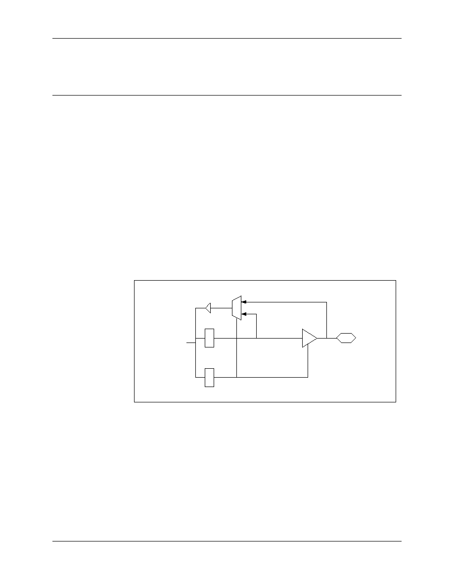
CX82100 Home Network Processor Data Sheet
101306C
Conexant Proprietary and Confidential Information
9-1
9
General Purpose Input/Output Interface Description
9.1
GPIO Pin Description
The GPIO pins can be read by reading GPIO_DATA_IN{x} register. They can be driven
as outputs by using GPIO_OE{x} for the pin driver enable, and GPIO_DATA_OUT{x}
for the data output polarity.
Each GPIO[x] pin is controlled individually by GPIO_OE{x} for the input/output
direction. All GPIO pins can serve as external interrupt inputs. These are controlled
through GPIO_ISR{x} and GPIO_IER{x} registers. The polarity and the sensitivity (i.e.,
edge or level) for each GPIO interrupt source can be controlled by programming the
GPIO_IPC{x} and GPIO_ISM{x} registers, respectively.
GPIO[39:37; 32] have alternate functions that can be controlled through the GPIO Option
Register (GPIO_OPT).
Figure 9-1 illustrates the internal interface for a GPIO pin.
Figure 9-1. GPIO[x] Interface
100545_061
GPIO[x]
GPIO_OE{x}
GPIO_DATA_OUT{x}
Local data bus
1
0
GPIO_DATA_IN{x}

CX82100 Home Network Processor Data Sheet
9-2
Conexant Proprietary and Confidential Information
101306C
9.2
GPIO Register Memory Map
GPIO registers are identified in Table 9-1.
Table 9-1. GPIO Registers
Register Label
Register Name
ASB Address
Type
Default Value
Ref.
GPIO_ISM1
GPIO Interrupt Sensitivity Mode Register 1
0x003500A0
RW
0x00000000
9.3.20
GPIO_ISM2
GPIO Interrupt Sensitivity Mode Register 2
0x003500A4
RW
0x00000000
9.3.21
GPIO_ISM3
GPIO Interrupt Sensitivity Mode Register 3
0x003500A8
RW
0x00000000
9.3.22
GPIO_OPT
GPIO Option Register
0x003500B0
RW
0x00000000
9.3.1
GPIO_OE1
GPIO Output Enable Register 1
0x003500B4
RW
0x00002306
9.3.2
GPIO_OE2
GPIO Output Enable Register 2
0x003500B8
RW
0x00000082
9.3.3
GPIO_OE3
GPIO Output Enable Register 3
0x003500BC
RW
0x00000000
9.3.4
GPIO_DATA_IN1
GPIO Data Input Register 1
0x003500C0
RO
0x00000000
9.3.5
GPIO_DATA_IN2
GPIO Data Input Register 2
0x003500C4
RO
0x00000000
9.3.6
GPIO_DATA_IN3
GPIO Data Input Register 3
0x003500C8
RO
0x00000000
9.3.7
GPIO_DATA_OUT1
GPIO Data Output Register 1
0x003500CC
RW
0x23062306
9.3.8
GPIO_DATA_OUT2
GPIO Data Output Register 2
0x003500D0
RW
0x00960086
9.3.9
GPIO_DATA_OUT3
GPIO Data Output Register 3
0x003500D4
RW
0x00000000
9.3.10
GPIO_ISR1
GPIO Interrupt Status Register 1
0x003500D8
RR
0x00000000
9.3.11
GPIO_ISR2
GPIO Interrupt Status Register 2
0x003500DC
RR
0x00000000
9.3.12
GPIO_ISR3
GPIO Interrupt Status Register 3
0x003500E0
RR
0x00000000
9.3.13
GPIO_IER1
GPIO Interrupt Enable Register 1
0x003500E4
RW
0x00000000
9.3.14
GPIO_IER2
GPIO Interrupt Enable Register 2
0x003500E8
RW
0x00000000
9.3.15
GPIO_IER3
GPIO Interrupt Enable Register 3
0x003500EC
RW
0x00000000
9.3.16
GPIO_IPC1
GPIO Interrupt Polarity Control Register 1
0x003500F0
RW
0x00000000
9.3.17
GPIO_IPC2
GPIO Interrupt Polarity Control Register 2
0x003500F4
RW
0x00000000
9.3.18
GPIO_IPC3
GPIO Interrupt Polarity Control Register 3
0x003500F8
RW
0x00000000
9.3.19

CX82100 Home Network Processor Data Sheet
101306C
Conexant Proprietary and Confidential Information
9-3
9.3
GPIO Registers
GPIO register bits are described in this section.
9.3.1
GPIO Option Register for GPIO[39:37; 32] (GPIO_OPT: 0x003500B0)
This register selects general or special purpose use for the GPIO[39:37; 32] pins.
Note:
Voltage levels for GPIO[39:37; 32] pins assigned to special purpose functions
by bits in the GPIO_OPT register are reflected in the GPIO_DATA_IN3
register, however, the GPIO_DATA_OUT3 register bits are not applicable.
Bit(s)
Type
Default
Name
Description
31:8
Reserved.
7
RW
1'b0
GPIO_Sel7
Select FCLKIO or GPIO39 Usage.
0 = FCLKIO/GPIO39 pin is used as GPIO39.
1 = FCLKIO/GPIO39 pin is used as FCLKIO.
Note:
Pin PLLBP high causes FCLKIO to be selected regardless of
this bit state.
6
RW
1'b0
GPIO_Sel6
Select BCLKIO or GPIO38 Usage.
0 = BCLKIO/GPIO38 pin is used as GPIO38.
1 = BCLKIO/GPIO38 pin is used as BCLKIO.
Note:
Pin PLLBP high causes BCLKIO to be selected regardless of
this bit state.
5
RW
1'b0
GPIO_Sel5
Select GPIO37 or HCS4# Usage.
0 = HAD31 (HCS4#)/GPIO37 pin is used as HCS4#.
1 = HAD31 (HCS4#)/GPIO37 pin is used as a GPIO37.
4:1
Reserved.
0
RW
1'b0
GPIO_Sel0
Select GPIO32 or HCS0# Usage.
0 = HC00 (HCS0#)/GPIO32 pin is used as HCS0#.
1 = HC00 (HCS0#)/GPIO32 pin is used as GPIO32.
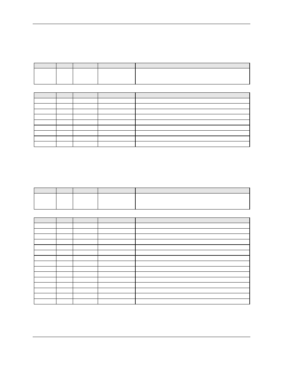
CX82100 Home Network Processor Data Sheet
9-4
Conexant Proprietary and Confidential Information
101306C
9.3.2
GPIO Output Enable Register 1 for GPIO[15:14; 8:5] (GPIO_OE1: 0x003500B4)
GPIO_OE1 is the output enable register for GPIO[15:14; 8:5].
Bit(s)
Type
Default
Name
Description
15:0;
15
Y0,
Y = Bit #
RW
16'b0
GPIO_OE{X},
15
X0,
X = Y
GPIO[X] Output Enable, 15
X0.
0 = GPIO[X] is an input pin.
1 = GPIO[X] is an output pin.
Bit(s)
Type
Default
Name
Description
31:16
Reserved.
15
RW
1'b0
GPIO_OE15
GPIO15 Output Enable.
14
RW
1'b0
GPIO_OE14
GPIO14 Output Enable.
13:9
Reserved.
8
RW
1'b0
GPIO_OE8
GPIO8 Output Enable.
7
RW
1'b0
GPIO_OE7
GPIO7 Output Enable.
6
RW
1'b0
GPIO_OE6
GPIO6 Output Enable.
5
RW
1'b0
GPIO_OE5
GPIO5 Output Enable.
4:0
Reserved.
9.3.3
GPIO Output Enable Register 2 for GPIO[31; 27:16] (GPIO_OE2: 0x003500B8)
GPIO_OE2 is the output enable register for GPIO[31; 27:16]
Bit(s)
Type
Default
Name
Description
15:0;
15
Y0,
Y = Bit #
RW
16'b0
GPIO_OE{X},
31
X16,
X = Y + 16
GPIO[X] Output Enable, 31
X16.
0 = GPIO[X] is an input pin.
1 = GPIO[X] is an output pin.
Bit(s)
Type
Default
Name
Description
31:16
Reserved.
15
RW
1'b0
GPIO_OE31
GPIO31 Output Enable.
14:12
Reserved.
11
RW
1'b0
GPIO_OE27
GPIO27 Output Enable.
10
RW
1'b0
GPIO_OE26
GPIO26 Output Enable.
9
RW
1'b0
GPIO_OE25
GPIO25 Output Enable.
8
RW
1'b0
GPIO_OE24
GPIO24 Output Enable.
7
Reserved.
6
RW
1'b0
GPIO_OE22
GPIO22 Output Enable.
5
RW
1'b0
GPIO_OE21
GPIO21 Output Enable.
4
RW
1'b0
GPIO_OE20
GPIO20 Output Enable.
3
RW
1'b0
GPIO_OE19
GPIO19 Output Enable.
2
RW
1'b0
GPIO_OE18
GPIO18 Output Enable.
1
RW
1
GPIO_OE17
GPIO17 Output Enable.
0
RW
1'b0
GPIO_OE16
GPIO16 Output Enable.
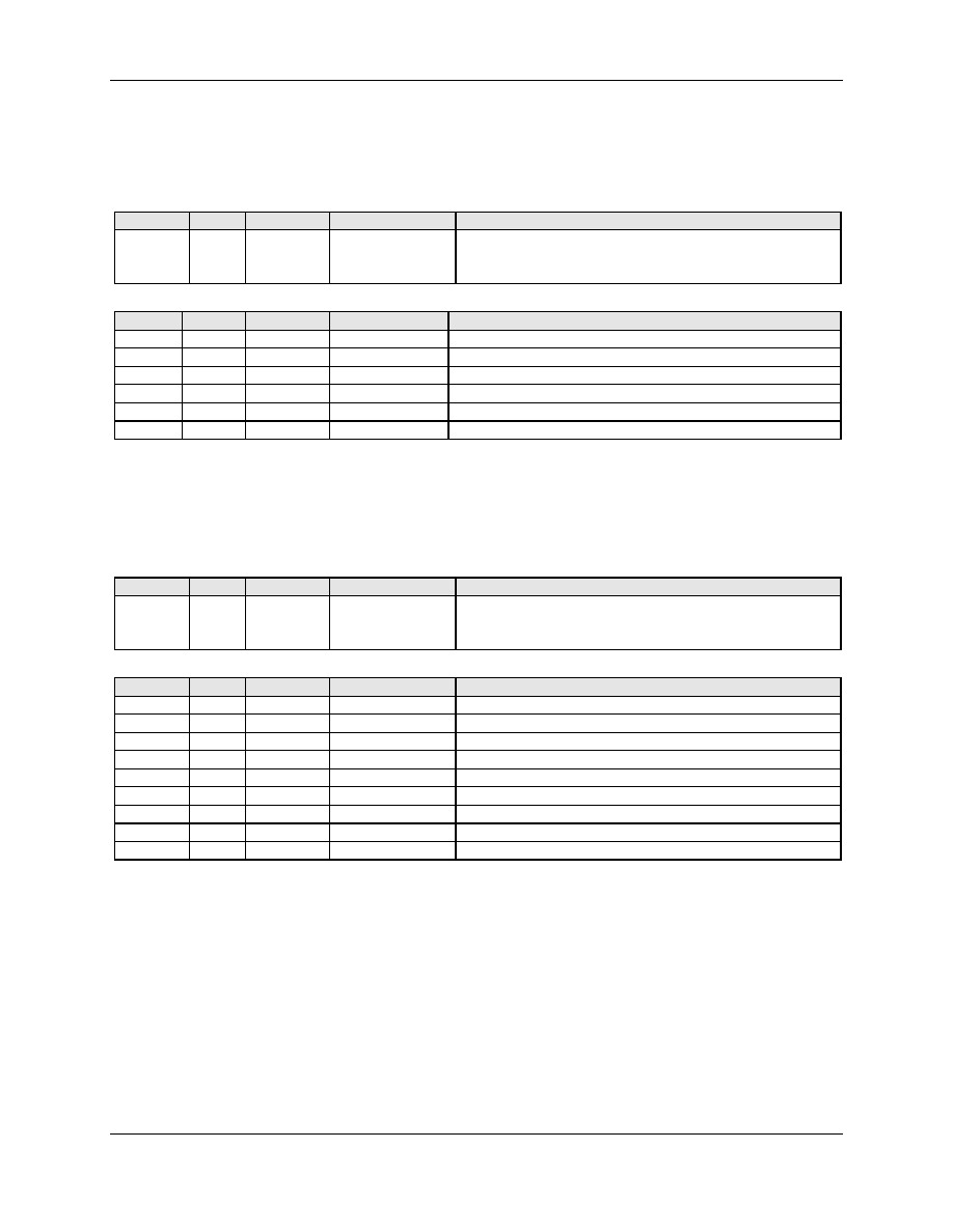
CX82100 Home Network Processor Data Sheet
101306C
Conexant Proprietary and Confidential Information
9-5
9.3.4
GPIO Output Enable Register 3 for GPIO[39:37; 32] (GPIO_OE3: 0x003500BC)
GPIO_OE3 is the output enable register for GPIO[39:37; 32].
Bit(s)
Type
Default
Name
Description
7:0;
7
Y0,
Y = Bit #
RW
8'b0
GPIO_OE{X},
39
X32,
X = Y + 32
GPIO[X] Output Enable, 39
X32.
0 = GPIO[X] is an input pin.
1 = GPIO[X] is an output pin.
Bit(s)
Type
Default
Name
Description
31:8
Reserved.
7
RW
1'b0
GPIO_OE39
GPIO39 Output Enable.
6
RW
1'b0
GPIO_OE38
GPIO38 Output Enable.
5
RW
1'b1
GPIO_OE37
GPIO37 Output Enable.
4:1
Reserved.
0
RW
1'b1
GPIO_OE32
GPIO32 Output Enable.
9.3.5
GPIO Data Input Register 1 for GPIO[15:14; 8:5] (GPIO_DATA_IN1: 0x003500C0)
GPIO_DATA_IN1is the data input register for GPIO[15:14; 8:5].
Bit(s)
Type
Default
Name
Description
15:0;
15
Y0,
Y = Bit #
RO
16'bx
GPIO_DIN {X},
15
X0,
X = Y
GPIO[X] Pin Voltage Level, 15
X0.
0 = Pin voltage level is low.
1 = Pin voltage level is high.
Bit(s)
Type
Name
Description
31:16
Reserved.
15
RO
1'bx
GPIO_DIN15
GPIO15 Pin Voltage Level.
14
RO
1'bx
GPIO_DIN14
GPIO14 Pin Voltage Level.
13:9
Reserved.
8
RO
1'bx
GPIO_DIN8
GPIO8 Pin Voltage Level.
7
RO
1'bx
GPIO_DIN7
GPIO7 Pin Voltage Level.
6
RO
1'bx
GPIO_DIN6
GPIO6 Pin Voltage Level.
5
RO
1'bx
GPIO_DIN5
GPIO5 Pin Voltage Level.
4:0
Reserved.
CX82100 Home Network Processor Data Sheet
9-6
Conexant Proprietary and Confidential Information
101306C
9.3.6
GPIO Data Input Register 2 for GPIO[31; 27:24; 22:16] (GPIO_DATA_IN2:
0x003500C4)
GPIO_DATA_IN2 is the data input register for GPIO[31; 27:24; 22:16].
Bit(s)
Type
Default
Name
Description
15:0;
15
Y0,
Y = Bit #
RO
16'bx
GPIO_DIN {X},
31
X16,
X = Y + 16
GPIO[X] Pin Voltage Level, 31
X16.
0 = Pin voltage level is low.
1 = Pin voltage level is high.
Bit(s)
Type
Name
Description
31:16
Reserved.
15
RO
1'bx
GPIO_DIN31
GPIO31 Pin Voltage Level.
14:12
Reserved.
11
RO
1'bx
GPIO_DIN27
GPIO27 Pin Voltage Level.
10
RO
1'bx
GPIO_DIN26
GPIO26 Pin Voltage Level.
9
Reserved.
8
RO
1'bx
GPIO_DIN24
GPIO24 Pin Voltage Level.
7
Reserved.
6
RO
1'bx
GPIO_DIN22
GPIO22 Pin Voltage Level.
5
RO
1'bx
GPIO_DIN21
GPIO21 Pin Voltage Level.
4
RO
1'bx
GPIO_DIN20
GPIO20 Pin Voltage Level.
3
RO
1'bx
GPIO_DIN19
GPIO19 Pin Voltage Level.
2
RO
1'bx
GPIO_DIN18
GPIO18 Pin Voltage Level.
1
RO
1'bx
GPIO_DIN17
GPIO17 Pin Voltage Level.
0
RO
1'bx
GPIO_DIN16
GPIO16 Pin Voltage Level.
9.3.7
GPIO Data Input Register 3 for GPIO[39:37; 32] (GPIO_DATA_IN3: 0x003500C8)
GPIO_DATA_IN3 is the data input register for GPIO[39:37; 32].
Bit(s)
Type
Default
Name
Description
7:0;
7
Y0,
Y = Bit #
RO
8'bx
GPIO_DIN {X},
39
X32,
X = Y + 32
GPIO[X] Pin Voltage Level, 39
X32.
0 = Pin voltage level is low.
1 = Pin voltage level is high.
Bit(s)
Type
Name
Description
31:8
Reserved.
7
RO
1'bx
GPIO_DIN39
GPIO39 Pin Voltage Level.
6
RO
1'bx
GPIO_DIN38
GPIO38 Pin Voltage Level.
5
RO
1'bx
GPIO_DIN37
GPIO37 Pin Voltage Level.
4:1
Reserved.
0
RO
1'bx
GPIO_DIN32
GPIO32 Pin Voltage Level.
CX82100 Home Network Processor Data Sheet
101306C
Conexant Proprietary and Confidential Information
9-7
9.3.8
GPIO Data Output Register 1 for GPIO[15:14; 8:5] (GPIO_DATA_OUT1:
0x003500CC)
The GPIO Data Output Register 1 contains read/write data output bits and corresponding
write-only output mask bits for GPIO[15:14; 8:5].
Writing a 1 to an output mask bit (GPIO_DOMSKx) enables the level corresponding to
associated data output bit (GPIO_DOUTx) onto the associated GPIO pin when the
associated direction bit (GPIO_OEx) is a 1; if the GPIO_OEx is a 0, there is no effect.
Writing a 0 to GPIO_DOMSKx has no effect.
Bit(s)
Type
Default
Name
Description
31:16;
31
Y16,
Y = Bit #
WO
16'b0
GPIO_DOMSK{X},
15
X0,
X = Y-16
GPIO[X] Output Mask, 15
X0.
Read:
Reads a 0.
Write:
GPIO_DOUT[X] (bit Y-16) mask (1 = Enable; 0 = Disable).
15:0;
15
Y0,
Y = Bit #
RW
16'bx
GPIO_DOUT{X},
15
X0,
X = Y
GPIO[X] Data Output, 15
X0.
Read:
Reads the last value written to this bit.
Write:
The output level (1 = high, 0 = low) is driven onto GPIO[X]
pin when mask bit is set (GPIO_DOMSK[X] = 1) and signal
direction is output (GPIO_OE[X] = 1); no effect, otherwise.
Bit(s)
Type
Default
Name
Description
31
WO
1'b0
GPIO_DOMSK15
GPIO15 Output Mask.
30
WO
1'b0
GPIO_DOMSK14
GPIO14 Output Mask.
29:25
Reserved.
24
WO
1'b1
GPIO_DOMSK8
GPIO8 Output Mask.
23
WO
1'b0
GPIO_DOMSK7
GPIO7 Output Mask.
22
WO
1'b0
GPIO_DOMSK6
GPIO6 Output Mask.
21
WO
1'b0
GPIO_DOMSK5
GPIO5 Output Mask.
20:16
Reserved.
15
RW
1'bx
GPIO_DOUT15
GPIO15 Data Output.
14
RW
1'bx
GPIO_DOUT14
GPIO14 Data Output.
13:9
Reserved.
8
RW
1'bx
GPIO_DOUT8
GPIO8 Data Output.
7
RW
1'bx
GPIO_DOUT7
GPIO7 Data Output.
6
RW
1'bx
GPIO_DOUT6
GPIO6 Data Output.
5
RW
1'bx
GPIO_DOUT5
GPIO5 Data Output.
4:0
Reserved.

CX82100 Home Network Processor Data Sheet
9-8
Conexant Proprietary and Confidential Information
101306C
9.3.9
GPIO Data Output Register 2 for GPIO[31; 27:24; 22:16] (GPIO_DATA_OUT2:
0x003500D0)
The GPIO Data Output Register 2 contains read/write data output bits and corresponding
write-only output mask bits for GPIO[31; 27:24; 22:16].
Writing a 1 to an output mask bit (GPIO_DOMSKx) enables the level corresponding to
associated data output bit (GPIO_DOUTx) onto the associated GPIO pin when the
associated direction bit (GPIO_OEx) is a 1; if the GPIO_OEx is a 0, there is no effect.
Writing a 0 to GPIO_DOMSKx has no effect.
Bit(s)
Type
Default
Name
Description
31:16;
31
Y16,
Y = Bit #
WO
16'b0
GPIO_DOMSK{X},
31
X16,
X = Y
GPIO[X] Output Mask, 31
X16.
Read:
Reads a 0.
Write:
GPIO_DOUT[X] (bit Y-16) mask (1 = Enable; 0 = Disable).
15:0;
15
Y0,
Y = Bit #
RW
16'bx
GPIO_DOUT{X},
31
X16,
X = Y +16
GPIO[X] Data Output, 31
X16.
Read:
Reads the last value written to this bit.
Write:
The output level (1 = high, 0 = low) is driven onto GPIO[X]
pin when mask bit is set (GPIO_DOMSK[X] = 1) and signal
direction is output (GPIO_OE[X] = 1); no effect, otherwise.
Bit(s)
Type
Default
Name
Description
31
WO
1'b0
GPIO_DOMSK31
GPIO31 Output Mask.
30:28
Reserved.
27
WO
1'b0
GPIO_DOMSK27
GPIO27 Output Mask.
26
WO
1'b0
GPIO_DOMSK26
GPIO26 Output Mask.
25
WO
1'b0
GPIO_DOMSK25
GPIO25 Output Mask.
24
WO
1'b0
GPIO_DOMSK24
GPIO24 Output Mask.
23
22
WO
1'b0
GPIO_DOMSK22
GPIO22 Output Mask.
21
WO
1'b0
GPIO_DOMSK21
GPIO21 Output Mask.
20
WO
1'b0
GPIO_DOMSK20
GPIO20 Output Mask.
19
WO
1'b0
GPIO_DOMSK19
GPIO19 Output Mask.
18
WO
1'b0
GPIO_DOMSK18
GPIO18 Output Mask.
17
WO
1'b1
GPIO_DOMSK17
GPIO17 Output Mask.
16
WO
1'b0
GPIO_DOMSK16
GPIO16 Output Mask.
15
RW
-
GPIO_DOUT31
GPIO31 Data Output.
14:12
Reserved.
11
RW
1'bx
GPIO_DOUT27
GPIO27 Data Output.
10
RW
1'bx
GPIO_DOUT26
GPIO26 Data Output.
9
RW
1'bx
GPIO_DOUT25
GPIO25 Data Output.
8
RW
1'bx
GPIO_DOUT24
GPIO24 Data Output.
7
Reserved.
6
RW
1'bx
GPIO_DOUT22
GPIO22 Data Output.
5
RW
1'bx
GPIO_DOUT21
GPIO21 Data Output.
4
RW
1'bx
GPIO_DOUT20
GPIO20 Data Output.
3
RW
1'bx
GPIO_DOUT19
GPIO19 Data Output.
2
RW
1'bx
GPIO_DOUT18
GPIO18 Data Output.
1
RW
1'bx
GPIO_DOUT17
GPIO17 Data Output.
0
RW
1'bx
GPIO_DOUT16
GPIO16 Data Output.

CX82100 Home Network Processor Data Sheet
101306C
Conexant Proprietary and Confidential Information
9-9
9.3.10
GPIO Data Output Register 3 for GPIO[39:37; 32] (GPIO_DATA_OUT3:
0x003500D4)
The GPIO Data Output Register 3 contains read/write data output bits and corresponding
write-only output mask bits for GPIO[39:32].
Writing a 1 to an output mask bit (GPIO_DOMSKx) enables the level corresponding to
associated data output bit (GPIO_DOUTx) onto the associated GPIO pin when the
associated direction bit (GPIO_OEx) is a 1; if the GPIO_OEx is a 0, there is no effect.
Writing a 0 to GPIO_DOMSKx has no effect.
Note:
Voltage levels for GPIO[39:37; 32] pins assigned to special purpose functions
by bits in the GPIO_OPT register are reflected in the GPIO_DATA_IN3
register, however, the GPIO_DATA_OUT3 register bits are not applicable.
Bit(s)
Type
Default
Name
Description
31:24
Reserved.
23:16;
23
Y16,
Y = Bit #
RO
8'b0
GPIO_DOMSK{X},
39
X32,
X = Y+16
GPIO[X] Output Mask, 39
X32.
Read:
Reads a 0.
Write:
GPIO_DOUT[X] (bit Y-=16) mask (1 = Enable; 0 = Disable).
15:8
Reserved.
7:0;
7
Y0,
Y = Bit #
RW
8'bx
GPIO_DOUT{X},
39
X32,
X = Y+32
GPIO[X] Data Output, 39
X32.
Read:
Reads the last value written to this bit.
Write:
The output level (1 = high, 0 = low) is driven onto GPIO[X]
pin when mask bit is set (GPIO_DOMSK[X] = 1) and signal
direction is output (GPIO_OE[X] = 1); no effect, otherwise.
Bit(s)
Type
Default
Name
Description
31:24
Reserved.
23
RO
1'b0
GPIO_DOMSK39
GPIO39 Output Mask.
22
RO
1'b0
GPIO_DOMSK38
GPIO38 Output Mask.
21
RO
1'b1
GPIO_DOMSK37
GPIO37 Output Mask.
20:17
Reserved.
16
RO
1'b1
GPIO_DOMSK32
GPIO32 Output Mask.
15:8
Reserved.
7
RW
-
GPIO_DOUT39
GPIO39 Data Output.
6
RW
-
GPIO_DOUT38
GPIO38 Data Output.
5
RW
1'b1
GPIO_DOUT37
GPIO37 Data Output.
4:1
Reserved.
0
RW
1'b1
GPIO_DOUT32
GPIO32 Data Output.
CX82100 Home Network Processor Data Sheet
9-10
Conexant Proprietary and Confidential Information
101306C
9.3.11
GPIO Interrupt Status Register 1 for GPIO[15:14; 8:5] (GPIO_ISR1: 0x003500D8)
GPIO_ISR1 is the interrupt input status register for GPIO[15:14; 8:5].
Note:
If an interrupt is level-sensitive, the corresponding status bit will remain a 1 as
long as the interrupt source is not removed. The status bit can be cleared only
after the interrupt source is removed and a 1 is written to the bit.
Bit(s)
Type
Default
Name
Description
15:0;
15
Y0,
Y = Bit #
RR
See specific
bit
GPIO_IS{X},
15
X0,
X = Y.
GPIO[X] Interrupt Status, 15
X0.
Reading:
bit #Y = 0 = > No interrupt detected on GPIO[X].
bit #Y = 1 = > Interrupt input detected on GPIO[X].
Writing:
0 to bit #Y = > no effect
1 to bit #Y = > clear the interrupt on GPIO[X].
Note:
If the interrupt is level-sensitive, the status bit will remain a 1 as
long as the interrupt resource is not removed. The bit can be cleared
only after the resource is removed and a 1 is written to it.
Bit(s)
Type
Default
Name
Description
15
RR
1'b0
GPIO_IS15
GPIO15 Interrupt Status.
14
RR
1'b0
GPIO_IS14
GPIO14 Interrupt Status.
13:9
Reserved.
8
RR
1'b0
GPIO_IS8
GPIO8 Interrupt Status.
7
RR
1'b0
GPIO_IS7
GPIO7 Interrupt Status.
6
RR
1'b0
GPIO_IS6
GPIO6 Interrupt Status.
5
RR
1'b0
GPIO_IS5
GPIO5 Interrupt Status.
4:0
Reserved.
9.3.12
GPIO Interrupt Status Register 2 for GPIO[31; 27:24; 22:16] (GPIO_ISR2:
0x003500DC)
GPIO_ISR2 is the interrupt input status register for GPIO[31; 27:16].
Note:
If an interrupt is level-sensitive, the corresponding status bit will remain a 1 as
long as the interrupt source is not removed. The status bit can be cleared only
after the interrupt source is removed and a 1 is written to the bit.
Bit(s)
Type
Default
Name
Description
CX82100 Home Network Processor Data Sheet
101306C
Conexant Proprietary and Confidential Information
9-11
Bit(s)
Type
Default
Name
Description
15:0;
15
Y0,
Y = Bit #
RR
See specific
bit
GPIO_IS{X},
31
X16,
X = Y+16.
GPIO[X] Interrupt Status, 31
X16.
Reading:
bit #Y = 0 = > No interrupt detected on GPIO[X].
bit #Y = 1 = > Interrupt input detected on GPIO[X].
Writing:
0 to bit #Y = > no effect
1 to bit #Y = > clear the interrupt on GPIO[X].
Note:
If the interrupt is level-sensitive, the status bit will remain a 1 as
long as the interrupt resource is not removed. The bit can be cleared
only after the resource is removed and a 1 is written to it.
Bit(s)
Type
Default
Name
Description
15
RR
1'b0
GPIO_IS31
GPIO31 Interrupt Status.
14:12
Reserved.
11
RR
1'b0
GPIO_IS27
GPIO27 Interrupt Status.
10
RR
1'b0
GPIO_IS26
GPIO26 Interrupt Status.
9
RR
1'b0
GPIO_IS25
GPIO25 Interrupt Status.
8
RR
1'b0
GPIO_IS24
GPIO24 Interrupt Status.
7
Reserved.
6
RR
1'b0
GPIO_IS22
GPIO22 Interrupt Status.
5
RR
1'b0
GPIO_IS21
GPIO21 Interrupt Status.
4
RR
1'b0
GPIO_IS20
GPIO20 Interrupt Status.
3
RR
1'b0
GPIO_IS19
GPIO19 Interrupt Status.
2
RR
1'b0
GPIO_IS18
GPIO18 Interrupt Status.
1
RR
1'b0
GPIO_IS17
GPIO17 Interrupt Status.
0
RR
1'b0
GPIO_IS16
GPIO16 Interrupt Status.
CX82100 Home Network Processor Data Sheet
9-12
Conexant Proprietary and Confidential Information
101306C
9.3.13
GPIO Interrupt Status Register 3 for GPIO[39:37; 32] (GPIO_ISR3: 0x003500E0)
GPIO_ISR3 is the interrupt input status register for GPIO[39:37; 32].
Note:
If an interrupt is level-sensitive, the corresponding status bit will remain a 1 as
long as the interrupt source is not removed. The status bit can be cleared only
after the interrupt source is removed and a 1 is written to the bit.
Bit(s)
Type
Default
Name
Description
7:0;
7
Y0,
Y = Bit #
RR
See specific
bit
GPIO_IS{X},
39
X32,
X = Y+32.
GPIO[X] Interrupt Status, 39
X32.
Reading:
bit #Y = 0 = > No interrupt detected on GPIO[X].
bit #Y = 1 = > Interrupt input detected on GPIO[X].
Writing:
0 to bit #Y = > no effect
1 to bit #Y = > clear the interrupt on GPIO[X].
Note:
If the interrupt is level-sensitive, the status bit will remain a 1 as
long as the interrupt resource is not removed. The bit can be cleared
only after the resource is removed and a 1 is written to it.
Bit(s)
Type
Default
Name
Description
31:8
Reserved.
7
RR
1'b0
GPIO_IS39
GPIO39 Interrupt Status.
6
RR
1'b0
GPIO_IS38
GPIO38 Interrupt Status.
5
RR
1'b0
GPIO_IS37
GPIO37 Interrupt Status.
4:1
Reserved.
0
RR
1'b0
GPIO_IS32
GPIO32 Interrupt Status.
CX82100 Home Network Processor Data Sheet
101306C
Conexant Proprietary and Confidential Information
9-13
9.3.14
GPIO Interrupt Enable Register 1 for GPIO[15:14; 8:5] (GPIO_IER1: 0x003500E4)
GPIO_IER1 is the interrupt input enable register for GPIO[15:14; 8:5].
Note:
If an interrupt input is enabled for GPIO[X], then GPIO[X] must be configured
as an input.
Bit(s)
Type
Default
Name
Description
31:16;
31
Y16,
Y = Bit #
RO
See specific
bit
GPIO_IEMSK{X},
15
X0,
X = Y-16.
GPIO[X] Interrupt Enable Mask, 15
X0.
Reading:
Return 0.
Writing:
0 = Mask off the function associated with GPIO_IE{X}.
1 = Enable the function associated with GPIO_IE{X}.
15:0;
15
Y0,
Y = Bit #
RW
See specific
bit
GPIO_IE{X},
15
X0,
X = Y.
GPIO[X] Interrupt Enable, 15
X0.
Reading:
Return the last value written to bit #Y.
Writing:
0 = Disable the GPIO[X] interrupt if GPIO_IEMSK{X} = 1; don't
care, otherwise.
1 = Enable the GPIO[X] interrupt if GPIO_IEMSK{X} = 1; don't
care, otherwise.
Bit(s)
Type
Default
Name
Description
31
RO
1'b0
GPIO_IEMSK15
GPIO15 Interrupt Enable Mask.
30
RO
1'b0
GPIO_IEMSK14
GPIO14 Interrupt Enable Mask.
29:25
Reserved.
24
RO
1'b0
GPIO_IEMSK8
GPIO8 Interrupt Enable Mask.
23
RO
1'b0
GPIO_IEMSK7
GPIO7 Interrupt Enable Mask.
22
RO
1'b0
GPIO_IEMSK6
GPIO6 Interrupt Enable Mask.
21
RO
1'b0
GPIO_IEMSK5
GPIO5 Interrupt Enable Mask.
20:16
Reserved.
15
RW
1'b0
GPIO_IE15
GPIO15 Interrupt Enable.
14
RW
1'b0
GPIO_IE14
GPIO14 Interrupt Enable.
13:9
Reserved.
8
RW
1'b0
GPIO_IE8
GPIO8 Interrupt Enable.
7
RW
1'b0
GPIO_IE7
GPIO7 Interrupt Enable.
6
RW
1'b0
GPIO_IE6
GPIO6 Interrupt Enable.
5
RW
1'b0
GPIO_IE5
GPIO5 Interrupt Enable.
4:0
Reserved.

CX82100 Home Network Processor Data Sheet
9-14
Conexant Proprietary and Confidential Information
101306C
9.3.15
GPIO Interrupt Enable Register 2 for GPIO[31; 27:24; 22:16] (GPIO_IER2:
0x003500E8)
GPIO_IER2 is the interrupt input enable register for GPIO[31:16]. Note that if an
interrupt input is enabled for GPIO[X], then GPIO[X] must be configured as an input.
Bit(s)
Type
Default
Name
Description
31:16;
31
Y16,
Y = Bit #
RO
See specific
bit
GPIO_IEMSK{X},
31
X16,
X = Y.
GPIO[X] Interrupt Enable Mask, 31
X16.
Reading:
Return 0.
Writing:
0 to bit #Y = > Mask off the function associated with GPIO_IE{X}.
1 to bit #Y = > Enable the function associated with GPIO_IE{X}.
15:0;
15
Y0,
Y = Bit #
RW
See specific
bit
GPIO_IE{X},
31
X16,
X = Y+16.
GPIO[X] Interrupt Enable, 31
X16.
Reading:
Return the last value written to bit #Y.
Writing:
0 to bit #Y = > Disable the GPIO[X] interrupt if GPIO_IEMSK{X} =
1; don't care, otherwise.
1 to bit #Y = > Enable the GPIO[X] interrupt if GPIO_IEMSK{X} =
1; don't care, otherwise.
Bit(s)
Type
Default
Name
Description
31
RO
1'b0
GPIO_IEMSK31
GPIO31 Interrupt Enable Mask.
30:28
Reserved.
27
RO
1'b0
GPIO_IEMSK27
GPIO27 Interrupt Enable Mask.
26
RO
1'b0
GPIO_IEMSK26
GPIO26 Interrupt Enable Mask.
25
RO
1'b0
GPIO_IEMSK25
GPIO25 Interrupt Enable Mask.
24
RO
1'b0
GPIO_IEMSK24
GPIO24 Interrupt Enable Mask.
23
Reserved.
22
RO
1'b0
GPIO_IEMSK22
GPIO22 Interrupt Enable Mask.
21
RO
1'b0
GPIO_IEMSK21
GPIO21 Interrupt Enable Mask.
20
RO
1'b0
GPIO_IEMSK20
GPIO20 Interrupt Enable Mask.
19
RO
1'b0
GPIO_IEMSK19
GPIO19 Interrupt Enable Mask.
18
RO
1'b0
GPIO_IEMSK18
GPIO18 Interrupt Enable Mask.
17
RO
1'b0
GPIO_IEMSK17
GPIO17 Interrupt Enable Mask.
16
RO
1'b0
GPIO_IEMSK16
GPIO16 Interrupt Enable Mask.
15
RO
1'b0
GPIO_IE31
GPIO31 Interrupt Enable.
14:12
Reserved.
11
RW
1'b0
GPIO_IE27
GPIO27 Interrupt Enable.
10
RW
1'b0
GPIO_IE26
GPIO26 Interrupt Enable.
9
RW
1'b0
GPIO_IE25
GPIO25 Interrupt Enable.
8
RW
1'b0
GPIO_IE24
GPIO24 Interrupt Enable.
7
Reserved.
6
RW
1'b0
GPIO_IE22
GPIO22 Interrupt Enable.
5
RW
1'b0
GPIO_IE21
GPIO21 Interrupt Enable.
4
RW
1'b0
GPIO_IE20
GPIO20 Interrupt Enable.
3
RW
1'b0
GPIO_IE19
GPIO19 Interrupt Enable.
2
RW
1'b0
GPIO_IE18
GPIO18 Interrupt Enable.
1
RW
1'b0
GPIO_IE17
GPIO17 Interrupt Enable.
0
RW
1'b0
GPIO_IE16
GPIO16 Interrupt Enable.
CX82100 Home Network Processor Data Sheet
101306C
Conexant Proprietary and Confidential Information
9-15
9.3.16
GPIO Interrupt Enable Register 3 for GPIO[39:37; 32] (GPIO_IER3: 0x003500EC)
GPIO_IER3 is the interrupt input enable register for GPIO[39:37; 32].
Note:
If an interrupt input is enabled for GPIO[X], then GPIO[X] must be configured
as an input.
Bit(s)
Type
Default
Name
Description
31:24
Reserved.
23:16;
23
Y16,
Y = Bit #
RO
See specific
bit
GPIO_IEMSK{X},
39
X32,
X = Y+16.
GPIO[X] Interrupt Enable Mask, 39
X32.
Reading:
Return 0.
Writing:
0 to bit #Y = > Mask off the function associated with GPIO_IE{X}.
1 to bit #Y = > Enable the function associated with GPIO_IE{X}.
15:8
Reserved.
7:0;
7
Y0,
Y = Bit #
RW
See specific
bit
GPIO_IE{X},
39
X32,
X = Y+32.
GPIO[X] Interrupt Enable, 39
X32.
Reading:
Return the last value written to bit #Y.
Writing:
0 to bit #Y = > Disable the GPIO[X] interrupt if GPIO_IEMSK{X} =
1; don't care, otherwise.
1 to bit #Y = > Enable the GPIO[X] interrupt if GPIO_IEMSK{X} =
1; don't care, otherwise.
Bit(s)
Type
Default
Name
Description
31:24
Reserved.
23
RO
1'b0
GPIO_IEMSK39
GPIO39 Interrupt Enable Mask.
22
RO
1'b0
GPIO_IEMSK38
GPIO38 Interrupt Enable Mask.
21
RO
1'b0
GPIO_IEMSK37
GPIO37 Interrupt Enable Mask.
20:17
Reserved.
16
RO
1'b0
GPIO_IEMSK32
GPIO32 Interrupt Enable Mask.
15:8
Reserved.
7
RW
1'b0
GPIO_IE39
GPIO39 Interrupt Enable.
6
RW
1'b0
GPIO_IE38
GPIO38 Interrupt Enable.
5
RW
1'b0
GPIO_IE37
GPIO37 Interrupt Enable.
4:1
Reserved.
0
RW
1'b0
GPIO_IE32
GPIO32 Interrupt Enable.
CX82100 Home Network Processor Data Sheet
9-16
Conexant Proprietary and Confidential Information
101306C
9.3.17
GPIO Interrupt Polarity Control Register 1 for GPIO[15:14; 8:5] (GPIO_IPC1:
0x003500F0)
GPIO_IPC1 is the interrupt polarity control register for GPIO[15:14; 8:5].
Bit(s)
Type
Default
Name
Description
31:16;
31
Y16,
Y = Bit #
RO
See specific
bit
GPIO_IPMSK{X},
15
X0,
X = Y-16.
GPIO[X] Interrupt Polarity Mask, 15
X0.
Reading:
Return 0.
Writing:
0 = Mask off the function associated with GPIO_IP{X}.
1 = Enable the function associated with GPIO_IP{X}.
15:0;
15
Y0,
Y = Bit #
RW
See specific
bit
GPIO_IP{X},
15
X0,
X = Y.
GPIO[X] Interrupt Polarity Control, 15
X0.
Reading:
Return the last value written to bit #Y.
Writing:
1 = For GPIO_IPMSK{X} = 1, interrupt will occur upon GPIO[X]
high or positive edge; for GPIO_IPMSK{X} = 0, interrupt will
not occur upon GPIO[X] high or positive edge.
0 = For GPIO_IPMSK{X} = 1, interrupt will occur upon GPIO[X]
low or negative edge; for GPIO_IPMSK{X} = 0, interrupt will
not occur upon GPIO[X] low or negative edge.
Bit(s)
Type
Default
Name
Description
31
RO
1'b0
GPIO_IPMSK15
GPIO15 Interrupt Polarity Mask.
30
RO
1'b0
GPIO_IPMSK14
GPIO14 Interrupt Polarity Mask.
29:25
Reserved.
24
RO
1'b0
GPIO_IPMSK8
GPIO8 Interrupt Polarity Mask.
23
RO
1'b0
GPIO_IPMSK7
GPIO7 Interrupt Polarity Mask.
22
RO
1'b0
GPIO_IPMSK6
GPIO6 Interrupt Polarity Mask.
21
RO
1'b0
GPIO_IPMSK5
GPIO5 Interrupt Polarity Mask.
20:16
Reserved.
15
RW
1'b0
GPIO_IP15
GPIO15 Interrupt Polarity Control.
14
RW
1'b0
GPIO_IP14
GPIO14 Interrupt Polarity Control.
13:9
Reserved.
8
RW
1'b0
GPIO_IP8
GPIO8 Interrupt Polarity Control.
7
RW
1'b0
GPIO_IP7
GPIO7 Interrupt Polarity Control.
6
RW
1'b0
GPIO_IP6
GPIO6 Interrupt Polarity Control.
5
RW
1'b0
GPIO_IP5
GPIO5 Interrupt Polarity Control.
4:0
Reserved.

CX82100 Home Network Processor Data Sheet
101306C
Conexant Proprietary and Confidential Information
9-17
9.3.18
GPIO Interrupt Polarity Control Register 2 for GPIO[31; 27:24; 22:16] (GPIO_IPC2:
0x003500F4)
GPIO_IPC2 is the interrupt polarity control register for GPIO[31; 27:24; 22:16].
Bit(s)
Type
Default
Name
Description
31:16;
31
Y16,
Y = Bit #
RO
See specific
bit
GPIO_IPMSK{X},
31
X16,
X = Y.
GPIO[X] Interrupt Polarity Mask, 31
X16.
Reading:
Return 0.
Writing:
0 = Mask off the function associated with GPIO_IP{X}.
1 = Enable the function associated with GPIO_IP{X}.
15:0;
15
Y0,
Y = Bit #
RW
See specific
bit
GPIO_IP{X},
31
X16,
X = Y+16.
GPIO[X] Interrupt Polarity Control, 31
X16.
Reading:
Return the last value written to bit #Y.
Writing:
1 = For GPIO_IPMSK{X} = 1, interrupt will occur upon GPIO[X]
high or positive edge; for GPIO_IPMSK{X} = 0, interrupt will
not occur upon GPIO[X] high or positive edge.
0 = For GPIO_IPMSK{X} = 1, interrupt will occur upon GPIO[X]
low or negative edge; for GPIO_IPMSK{X} = 0, interrupt will
not occur upon GPIO[X] low or negative edge.
Bit(s)
Type
Default
Name
Description
31
RO
1'b0
GPIO_IPMSK31
GPIO31 Interrupt Polarity Mask.
30:28
Reserved.
27
RO
1'b0
GPIO_IPMSK27
GPIO27 Interrupt Polarity Mask.
26
RO
1'b0
GPIO_IPMSK26
GPIO26 Interrupt Polarity Mask.
25
RO
1'b0
GPIO_IPMSK25
GPIO25 Interrupt Polarity Mask.
24
RO
1'b0
GPIO_IPMSK24
GPIO24 Interrupt Polarity Mask.
23
Reserved.
22
RO
1'b0
GPIO_IPMSK22
GPIO22 Interrupt Polarity Mask.
21
RO
1'b0
GPIO_IPMSK21
GPIO21 Interrupt Polarity Mask.
20
RO
1'b0
GPIO_IPMSK20
GPIO20 Interrupt Polarity Mask.
19
RO
1'b0
GPIO_IPMSK19
GPIO19 Interrupt Polarity Mask.
18
RO
1'b0
GPIO_IPMSK18
GPIO18 Interrupt Polarity Mask.
17
RO
1'b0
GPIO_IPMSK17
GPIO17 Interrupt Polarity Mask.
16
RO
1'b0
GPIO_IPMSK16
GPIO16 Interrupt Polarity Mask.
15
RW
1'b0
GPIO_IP31
GPIO31 Interrupt Polarity Control.
14:12
Reserved.
11
RW
1'b0
GPIO_IP27
GPIO27 Interrupt Polarity Control.
10
RW
1'b0
GPIO_IP26
GPIO26 Interrupt Polarity Control.
9
RW
1'b0
GPIO_IP25
GPIO25 Interrupt Polarity Control.
8
RW
1'b0
GPIO_IP24
GPIO24 Interrupt Polarity Control.
7
Reserved.
6
RW
1'b0
GPIO_IP22
GPIO22 Interrupt Polarity Control.
5
RW
1'b0
GPIO_IP21
GPIO21 Interrupt Polarity Control.
4
RW
1'b0
GPIO_IP20
GPIO20 Interrupt Polarity Control.
3
RW
1'b0
GPIO_IP19
GPIO19 Interrupt Polarity Control.
2
RW
1'b0
GPIO_IP18
GPIO18 Interrupt Polarity Control.
1
RW
1'b0
GPIO_IP17
GPIO17 Interrupt Polarity Control.
0
RW
1'b0
GPIO_IP16
GPIO16 Interrupt Polarity Control.

CX82100 Home Network Processor Data Sheet
9-18
Conexant Proprietary and Confidential Information
101306C
9.3.19
GPIO Interrupt Polarity Control Register 3 for GPIO[39:37; 32] (GPIO_IPC3:
0x003500F8)
GPIO_IPC3 is the interrupt polarity control register for GPIO[39:37; 32].
Bit(s)
Type
Default
Name
Description
31:24
Reserved.
23:16;
23
Y16,
Y = Bit #
RO
See specific
bit
GPIO_IPMSK{X},
39
X32,
X = Y+16.
GPIO[X] Interrupt Polarity Mask, 39
X32.
Reading:
Return 0.
Writing:
0 = Mask off the function associated with GPIO_IP{X}.
1 = Enable the function associated with GPIO_IP{X}.
15:8
Reserved.
7:0;
7
Y0,
Y = Bit #
RW
See specific
bit
GPIO_IP{X},
39
X32,
X = Y+32.
GPIO[X] Interrupt Polarity Control, 39
X32.
Reading:
Return the last value written to bit #Y.
Writing:
1 = For GPIO_IPMSK{X} = 1, interrupt will occur upon GPIO[X]
high or positive edge; for GPIO_IPMSK{X} = 0, interrupt will
not occur upon GPIO[X] high or positive edge.
0 = For GPIO_IPMSK{X} = 1, interrupt will occur upon GPIO[X]
low or negative edge; for GPIO_IPMSK{X} = 0, interrupt will
not occur upon GPIO[X] low or negative edge.
Bit(s)
Type
Default
Name
Description
31:24
Reserved.
23
RO
1'b0
GPIO_IPMSK39
GPIO39 Interrupt Polarity Mask.
22
RO
1'b0
GPIO_IPMSK38
GPIO38 Interrupt Polarity Mask.
21
RO
1'b0
GPIO_IPMSK37
GPIO37 Interrupt Polarity Mask.
20:17
Reserved.
16
RO
1'b0
GPIO_IPMSK32
GPIO32 Interrupt Polarity Mask.
15:8
Reserved.
7
RW
1'b0
GPIO_IP39
GPIO39 Interrupt Polarity Control.
6
RW
1'b0
GPIO_IP38
GPIO38 Interrupt Polarity Control.
5
RW
1'b0
GPIO_IP37
GPIO37 Interrupt Polarity Control.
4:1
Reserved.
0
RW
1'b0
GPIO_IP32
GPIO32 Interrupt Polarity Control.
CX82100 Home Network Processor Data Sheet
101306C
Conexant Proprietary and Confidential Information
9-19
9.3.20
GPIO Interrupt Sensitivity Mode Register 1 for GPIO[15:14; 8:5] (GPIO_ISM1:
0x003500A0)
GPIO_ISM1 is the interrupt sensitive mode register for GPIO[15:14; 8:5].
Bit(s)
Type
Default
Name
Description
31:16;
31
Y16,
Y = Bit #
RO
See specific
bit
GPIO_ISMMSK{X},
15
X0,
X = Y-16.
GPIO[X] Interrupt Sensitivity Mode Mask, 15
X0.
Reading:
Return 0.
Writing:
0= Mask off the function associated with GPIO_ISMC{X}.
1 = Enable the function associated with GPIO_ISMC{X}.
15:0;
15
Y0,
Y = Bit #
RW
See specific
bit
GPIO_ISMC{X},
15
X0,
X = Y.
GPIO[X] Interrupt Sensitivity Mode Control, 15
X0.
Reading:
Return the last value written to bit #Y.
Writing:
1 = Interrupt input on GPIO[X] will be edge sensitive, if
GPIO_ISMMSK{X} = 1; don't care, otherwise.
0 = Interrupt input on GPIO[X] will be level sensitive, if
GPIO_ISMMSK{X} = 1; don't care, otherwise.
Bit(s)
Type
Default
Name
Description
31
RO
1'b0
GPIO_ISMMSK15
GPIO15 Interrupt Sensitivity Mode Mask.
30
RO
1'b0
GPIO_ISMMSK14
GPIO14 Interrupt Sensitivity Mode Mask.
29:25
Reserved.
24
RO
1'b0
GPIO_ISMMSK8
GPIO8 Interrupt Sensitivity Mode Mask.
23
RO
1'b0
GPIO_ISMMSK7
GPIO7 Interrupt Sensitivity Mode Mask.
22
RO
1'b0
GPIO_ISMMSK6
GPIO6 Interrupt Sensitivity Mode Mask.
21
RO
1'b0
GPIO_ISMMSK5
GPIO5 Interrupt Sensitivity Mode Mask.
20:16
Reserved.
15
RW
1'b0
GPIO_ISMC15
GPIO15 Interrupt Sensitivity Mode Control.
14
RW
1'b0
GPIO_ISMC14
GPIO14 Interrupt Sensitivity Mode Control.
13:9
Reserved.
8
RW
1'b0
GPIO_ISMC8
GPIO8 Interrupt Sensitivity Mode Control.
7
RW
1'b0
GPIO_ISMC7
GPIO7 Interrupt Sensitivity Mode Control.
6
RW
1'b0
GPIO_ISMC6
GPIO6 Interrupt Sensitivity Mode Control.
5
RW
1'b0
GPIO_ISMC5
GPIO5 Interrupt Sensitivity Mode Control.
4:0
Reserved.

CX82100 Home Network Processor Data Sheet
9-20
Conexant Proprietary and Confidential Information
101306C
9.3.21
GPIO Interrupt Sensitivity Mode Register 2 for GPIO[31; 27:24; 22:16]
(GPIO_ISM2: 0x003500A4)
GPIO_ISM2 is the interrupt sensitive mode register for GPIO[31; 27:24; 22:16].
Bit(s)
Type
Default
Name
Description
31:16;
31
Y16,
Y = Bit #
RO
See specific
bit
GPIO_ISMMSK{X},
31
X16,
X = Y.
GPIO[X] Interrupt Sensitivity Mode Mask, 31
X16.
Reading:
Return 0.
Writing:
0= Mask off the function associated with GPIO_ISMC{X}.
1 = Enable the function associated with GPIO_ISMC{X}.
15:0;
15
Y0,
Y = Bit #
RW
See specific
bit
GPIO_ISMC{X},
31
X16,
X = Y+16.
GPIO[X] Interrupt Sensitivity Mode Control, 31
X16.
Reading:
Return the last value written to bit #Y.
Writing:
1 = Interrupt input on GPIO[X] will be edge sensitive, if
GPIO_ISMMSK{X} = 1; don't care, otherwise.
0 = Interrupt input on GPIO[X] will be level sensitive, if
GPIO_ISMMSK{X} = 1; don't care, otherwise.
Bit(s)
Type
Default
Name
Description
31
RO
1'b0
GPIO_ISMMSK31
GPIO31 Interrupt Sensitivity Mode Mask.
30:28
Reserved.
27
RO
1'b0
GPIO_ISMMSK27
GPIO27 Interrupt Sensitivity Mode Mask.
26
RO
1'b0
GPIO_ISMMSK26
GPIO26 Interrupt Sensitivity Mode Mask.
25
RO
1'b0
GPIO_ISMMSK25
GPIO25 Interrupt Sensitivity Mode Mask.
24
RO
1'b0
GPIO_ISMMSK24
GPIO24 Interrupt Sensitivity Mode Mask.
23
Reserved.
22
RO
1'b0
GPIO_ISMMSK22
GPIO22 Interrupt Sensitivity Mode Mask.
21
RO
1'b0
GPIO_ISMMSK21
GPIO21 Interrupt Sensitivity Mode Mask.
20
RO
1'b0
GPIO_ISMMSK20
GPIO20 Interrupt Sensitivity Mode Mask.
19
RO
1'b0
GPIO_ISMMSK19
GPIO19 Interrupt Sensitivity Mode Mask.
18
RO
1'b0
GPIO_ISMMSK18
GPIO18 Interrupt Sensitivity Mode Mask.
17
RO
1'b0
GPIO_ISMMSK17
GPIO17 Interrupt Sensitivity Mode Mask.
16
RO
1'b0
GPIO_ISMMSK16
GPIO16 Interrupt Sensitivity Mode Mask.
15
RW
1'b0
GPIO_ISMC31
GPIO31 Interrupt Sensitivity Mode Control.
14
RW
1'b0
GPIO_ISMC30
GPIO30 Interrupt Sensitivity Mode Control.
13
RW
1'b0
GPIO_ISMC29
GPIO29 Interrupt Sensitivity Mode Control.
12
RW
1'b0
GPIO_ISMC28
GPIO28 Interrupt Sensitivity Mode Control.
11
RW
1'b0
GPIO_ISMC27
GPIO27 Interrupt Sensitivity Mode Control.
10
RW
1'b0
GPIO_ISMC26
GPIO26 Interrupt Sensitivity Mode Control.
9
RW
1'b0
GPIO_ISMC25
GPIO25 Interrupt Sensitivity Mode Control.
8
RW
1'b0
GPIO_ISMC24
GPIO24 Interrupt Sensitivity Mode Control.
7
RW
1'b0
GPIO_ISMC23
GPIO23 Interrupt Sensitivity Mode Control.
6
RW
1'b0
GPIO_ISMC22
GPIO22 Interrupt Sensitivity Mode Control.
5
RW
1'b0
GPIO_ISMC21
GPIO21 Interrupt Sensitivity Mode Control.
4
RW
1'b0
GPIO_ISMC20
GPIO20 Interrupt Sensitivity Mode Control.
3
RW
1'b0
GPIO_ISMC19
GPIO19 Interrupt Sensitivity Mode Control.
2
RW
1'b0
GPIO_ISMC18
GPIO18 Interrupt Sensitivity Mode Control.
1
RW
1'b0
GPIO_ISMC17
GPIO17 Interrupt Sensitivity Mode Control.
0
RW
1'b0
GPIO_ISMC16
GPIO16 Interrupt Sensitivity Mode Control.
CX82100 Home Network Processor Data Sheet
101306C
Conexant Proprietary and Confidential Information
9-21
9.3.22
GPIO Interrupt Sensitivity Mode Register 3 for GPIO[39:37; 32] (GPIO_ISM3:
0x003500A8)
GPIO_ISM2 is the interrupt sensitive mode register for GPIO[39:37; 32].
Bit(s)
Type
Default
Name
Description
31:24
Reserved.
23:16;
23
Y16,
Y = Bit #
RO
See specific
bit
GPIO_ISMMSK{X},
39
X32,
X = Y+16.
GPIO[X] Interrupt Sensitivity Mode Mask, 39
X32.
Reading:
Return 0.
Writing:
0= Mask off the function associated with GPIO_ISMC{X}.
1 = Enable the function associated with GPIO_ISMC{X}.
15:8
Reserved.
7:0;
7
Y0,
Y = Bit #
RW
See specific
bit
GPIO_ISMC{X},
39
X32,
X = Y+32.
GPIO[X] Interrupt Sensitivity Mode Control, 39
X32.
Reading:
Return the last value written to bit #Y.
Writing:
1 = Interrupt input on GPIO[X] will be edge sensitive, if
GPIO_ISMMSK{X} = 1; don't care, otherwise.
0 = Interrupt input on GPIO[X] will be level sensitive, if
GPIO_ISMMSK{X} = 1; don't care, otherwise.
Bit(s)
Type
Default
Name
Description
31:24
Reserved.
23
RO
1'b0
GPIO_ISMMSK39
GPIO39 Interrupt Sensitivity Mode Mask.
22
RO
1'b0
GPIO_ISMMSK38
GPIO38 Interrupt Sensitivity Mode Mask.
21
RO
1'b0
GPIO_ISMMSK37
GPIO37 Interrupt Sensitivity Mode Mask.
20:17
Reserved.
16
RO
1'b0
GPIO_ISMMSK32
GPIO32 Interrupt Sensitivity Mode Mask.
15:8
Reserved.
7
RW
1'b0
GPIO_ISMC39
GPIO39 Interrupt Sensitivity Mode Control.
6
RW
1'b0
GPIO_ISMC38
GPIO38 Interrupt Sensitivity Mode Control.
5
RW
1'b0
GPIO_ISMC37
GPIO37 Interrupt Sensitivity Mode Control.
4:1
Reserved.
0
RW
1'b0
GPIO_ISMC32
GPIO32 Interrupt Sensitivity Mode Control.

CX82100 Home Network Processor Data Sheet
9-22
Conexant Proprietary and Confidential Information
101306C
This page is intentionally blank.
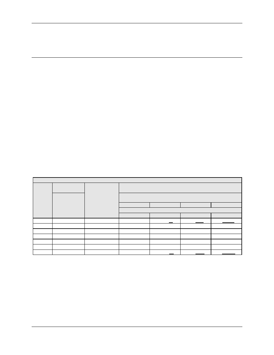
CX82100 Home Network Processor Data Sheet
101306C
Conexant Proprietary and Confidential Information
10-1
10
Memory to Memory Transfer Input/Output
10.1
Operation
A qword buffer resides within this block to support memory to memory block transfers.
Data transfer requests are issued to the DMAC via channel 7 for reading from the source
buffer and channel 8 for writing to the destination buffer. The number of qwords to
transfer is set by M2M_Cntl. This count is big enough to initialize the entire 8 MB of
external SDRAM if desired. When M2M_Cntl is set to 0, or counts down to 0, the DMA
block transfer is done. An interrupt is set (INT_Stat:8) when the DMAC completes the
data block transfer. If M2M_DO is set, then only write transfers will occur to the
destination buffer. Since the ARM can also write to the DMA port buffer M2M_DMA, it
could use the DMAC to initialize memory to any constant.
The memory-to-memory transfer always consists of an integer number of qwords. The
source and destination addresses are always dword-aligned. Little-endian byte-
realignment is supported by using M2M_BS and using firmware for cleaning up the end
conditions. Some examples for M2M data transfers are shown in Table 10-1, Table 10-2,
and Table 10-3. The bytes highlighted in bold have to be copied or restored by firmware.
Table 10-1. M2M Transfer Example 1
M2M Data Transfer Example
Source Memory
to Copy: 24B
Destination Memory after Copy
M2M_Cnt = 3 qwords, DMA8_Ptr1 = 00
Start Source
Byte-Address
Start Destination Byte-Address
0
1
2
3
M2M_BS, DMA7_Ptr1
Byte
Address
0
Destination
Memory before
Copy
0, 00
1, 00
2, 00
3, 00
00
03020100
FFFFFFFF
03020100
020100xx
0100xxxx
00xxxxxx
04
07060504
FFFFFFFF
07060504
06050403
05040302
04030201
08
0B0A0908
FFFFFFFF
0B0A0908
0A090807
09080706
08070605
0C
0F0E0D0C
FFFFFFFF
0F0E0D0C
0E0D0C0B
0D0C0B0A
0C0B0A09
10
13121110
FFFFFFFF
13121110
1211100F
11100F0E
100F0E0D
14
17161514
FFFFFFFF
17161514
16151413
15141312
14131211
18
1B1A1918
FFFFFFFF
FFFFFFFF
FFFFFFFF
FFFFFFFF
FFFFFFFF
CX82100 Home Network Processor Data Sheet
10-2
Conexant Proprietary and Confidential Information
101306C
Table 10-2. M2M Transfer Example 2
M2M Data Transfer Example
Source Memory
to Copy: 24B
Destination Memory after Copy
M2M_Cnt = 3 qwords, DMA8_Ptr1 = 00
Start Source
Byte-Address
Start Destination Byte-Address
0
1
2
3
M2M_BS, DMA7_Ptr1
Byte
Address
1
Destination
Memory before
Copy
3, 04
0, 00
1, 00
2, 00
00
03020100
FFFFFFFF
04xxxxxx
03020100
020100xx
0100xxxx
04
07060504
FFFFFFFF
08070605
07060504
06050403
05040302
08
0B0A0908
FFFFFFFF
0C0B0A09
0B0A0908
0A090807
09080706
0C
0F0E0D0C
FFFFFFFF
100F0E0D
0F0E0D0C
0E0D0C0B
0D0C0B0A
10
13121110
FFFFFFFF
14131211
13121110
1211100F
11100F0E
14
17161514
FFFFFFFF
18171615
17161514
16151413
15141312
18
1B1A19
18
FFFFFFFF
FFFFFFFF
FFFFFFFF
FFFFFFFF
FFFFFFFF
Table 10-3. M2M Transfer Example 3
M2M Data Transfer Example
Source Memory
to Copy: 24B
Destination Memory after Copy
M2M_Cnt = 3 qwords, DMA8_Ptr1 = 00
Start Source
Byte-Address
Start Destination Byte-Address
0
1
2
3
M2M_BS, DMA7_Ptr1
Byte
Address
3
Destination
Memory before
Copy
1, 04
2, 04
3, 04
0, 00
00
03020100
FFFFFFFF
060504xx
0504xxxx
04xxxxxx
03020100
04
07060504
FFFFFFFF
0A090807
09080706
08070605
07060504
08
0B0A0908
FFFFFFFF
0E0D0C0B
0D0C0B0A
0C0B0A09
0B0A0908
0C
0F0E0D0C
FFFFFFFF
1211100F
11100F0E
100F0E0D
0F0E0D0C
10
13121110
FFFFFFFF
16151413
15141312
14131211
13121110
14
17161514
FFFFFFFF
1A191817
19181716
18171615
17161514
18
1B
1A1918
FFFFFFFF
FFFFFFFF
FFFFFFFF
FFFFFFFF
FFFFFFFF
When doing a multiple qword buffer transfer there are actually 128 cases to consider for
byte re-alignment. This # of permutations results from 4 start byte src-locations, 8 end
byte src-locations, and 4 start byte dst-locations (4x8x4 = 128). The start/end src-
locations bound the buffer size for transfer. The firmware will need to fix the corrupted
first dword (save original dst-1
st
-loc before copy), and also supply the last byte-merged 1-
2 dwords.

CX82100 Home Network Processor Data Sheet
101306C
Conexant Proprietary and Confidential Information
10-3
10.2
M2M Register Memory Map
M2M registers are identified in Table 10-4
Table 10-4. M2M Registers
Register Label
Register Name
ASB Address
Type
Default Value
Ref.
M2M_DMA
Memory to Memory DMA Data Register
0x00350000
RWp
64'bx
10.3.1
M2M_Cntl
Memory to Memory DMA Transfer
Control/Counter
0x00350004
RW
0x00000000
10.3.2
10.3
M2M Registers
10.3.1
Memory to Memory DMA Data Register (M2M_DMA: 0x00350000)
Bit(s)
Type
Default
Name
Description
63:0
RWp
64'bx
M2M_DMA
A single qword buffer for DMA source/destination access.
10.3.2
Memory to Memory DMA Transfer Control/Counter (M2M_Cntl: 0x00350004)
Bit(s)
Type
Default
Name
Description
22:21
RW
2'b0
M2M_BS
Memory to Memory Bytes to Lag Data or Shift Left.
No. of bytes to lag data or shift left. Useful for little-endian
byte re-alignment.
20
RW
1'b0
M2M_DO
Disabled Memory to Memory Source Transfers.
0 = Enable source and destination transfers.
1 = Disable source transfers, and enable only
destination transfers.
19:0
RW
20'b0
M2M_Cnt
Memory to Memory Count.
No. of qwords to transfer.

CX82100 Home Network Processor Data Sheet
10-4
Conexant Proprietary and Confidential Information
101306C
This page is intentionally blank.
CX82100 Home Network Processor Data Sheet
101306C
Conexant Proprietary and Confidential Information
11-1
11
Interrupt Controller Interface Description
All peripheral interrupt sources are routed through the Interrupt Controller (INTC) and
reduced to one of two active low inputs to the ARM940T processor, fast interrupt (FIQ#)
or regular interrupt (IRQ#), as selected in the Interrupt Level Assignment Register
(INT_LA). No hardware-assisted priority scheme is implemented in the HNP other than
FIQ# having a higher priority than IRQ#. The system software must implement the
priority scheme for individual interrupts in the FIQ# and IRQ# exception handlers.
11.1
INTC Register Memory Map
INTC registers are identified in Table 11-1.
Table 11-1. INTC Registers
Register Label
Register Name
ASB Address
Type
Default Value
Ref.
INT_LA
Interrupt Level Assignment Register
0x00350040
RW
0x00000000
11.2.1
INT_Stat
Interrupt Status Register
0x00350044
RR
0x00000000
11.2.2
INT_SetStat
Interrupt Set Status Register
0x00350048
WO
0x00000000
11.2.3
INT_Msk
Interrupt Mask Register
0x0035004C
RW
0x00000000
11.2.4
INT_Mstat
Interrupt Mask Status Register
0x00350090
RO
0x00000000
11.2.5
11.2
INTC Registers
11.2.1
Interrupt Level Assignment Register (INT_LA: 0x00350040)
The INTC receives an interrupt signal from a potential interrupt source and compares it
with the corresponding interrupt level assignment register (INT_LA) to determine if a
fast interrupt (FIQ#) signal or a regular interrupt (IRQ#) signal should be sent to the
ARM940T processor. Setting the interrupt's corresponding bit on the Interrupt Level
Assignment Register to a 1 will cause a FIQ# interrupt, while a 0 will cause an IRQ#
interrupt.
Bit
Type
Default
Name
Description
31:0
RW
32'h00000000
Int_LA_x
Level Assignment Interrupt Control.
0 = The corresponding bit location in the INT_Stat register will cause
an IRQ# interrupt to the INTC if the interrupt has been enabled.
1 = The corresponding bit location in the INT_Stat register will cause
a FIQ# interrupt to the INTC if the interrupt has been enabled.

CX82100 Home Network Processor Data Sheet
11-2
Conexant Proprietary and Confidential Information
101306C
11.2.2
Interrupt Status Register (INT_Stat: 0x00350044)
Each interrupt source sets a bit in the interrupt status register (INT_Stat). These pending
interrupts can be read at anytime. If a bit in this register represents multiple interrupt
sources, then it is read-only. Most bits are automatically cleared once all the
corresponding interrupt sources are cleared, however, bits 19 and 20 are not
automatically cleared. Any other bit in this register can be cleared by writing a one to the
same bit location. (Note that in some cases, the interrupt source in the peripheral must be
cleared before the clearing of the corresponding interrupt bit in this register can take
effect.).
Writing a zero has no effect.
Bit
Type
Default
Name
Description
31
RR
1'b0
Int_SW3
Software Interrupt 3.
0 = Interrupt condition has not occurred.
1 = The corresponding data bit has been set high when writing
to INT_SetStat.
30
RR
1'b0
Int_SW2
Software Interrupt 2.
0 = Interrupt condition has not occurred.
1 = The corresponding data bit has been set high when writing
to INT_SetStat.
29
RR
1'b0
Int_SW1
Software Interrupt 1.
0 = Interrupt condition has not occurred.
1 = The corresponding data bit has been set high when writing
to INT_SetStat.
28
RR
1'b0
Int_SW0
Software Interrupt 0.
0 = Interrupt condition has not occurred.
1 = The corresponding data bit has been set high when writing
to INT_SetStat.
27
RR
1'b0
Int_COMMRX
ARM9 Communication RXD Channel Interrupt.
0 = The receive buffer does not contain data waiting to be
read.
1 = The ARM9 communication RXD channel (between
processor and the debugger) receive buffer contains data
waiting to be read.
26
RR
1'b0
Int_COMMTX
ARM9 Communication TXD channel Interrupt.
0 = The transmit buffer is not empty.
1 = The ARM9 communication TXD channel (between
processor and the debugger) transmit buffer is empty.
25
Reserved.
24
RO
1'b0
Int_GPIO
GPIO Interrupt.
0 = Interrupt condition has not occurred.
1 = An external interrupt through a GPIO input pin has
occurred.
23:21
Reserved.
20
RR
1'b0
Int_EMAC#2_ERR
EMAC 2 Exception Condition Interrupt.
0 = Interrupt condition has not occurred.
1 = EMAC 2 receiver or transmitter detected a normal or
abnormal exception condition. Must be written to be
cleared.
19
RR
1'b0
Int_EMAC#1_ERR
EMAC 1 Exception Condition Interrupt.
0 = Interrupt condition has not occurred.
1 = EMAC 1 receiver or transmitter detected a normal or
abnormal exception condition. Must be written to be
cleared.

CX82100 Home Network Processor Data Sheet
101306C
Conexant Proprietary and Confidential Information
11-3
Bit
Type
Default
Name
Description
18
RR
1'b0
Int_DMAC_ERR
DMAC BERROR Interrupt
0 = Interrupt condition has not occurred.
1 = The BERROR signal has been asserted to the DMAC ASB
master.
17:16
Reserved.
15
RR
1'b0
Int_DMAC_EMAC#1_TX
DMA Channel 1 Transfer Complete Interrupt.
0 = Interrupt condition has not occurred.
1 = DMAC completed a block/packet transfer to EMAC 1.
14
RR
1'b0
Int_DMAC_EMAC#1_RX
DMA Channel 2 Transfer Complete Interrupt.
0 = Interrupt condition has not occurred.
1 = DMAC completed a block/packet transfer from EMAC 1.
13
RR
1'b0
Int_DMAC_EMAC#2_TX
DMA Channel 3 Transfer Complete Interrupt.
0 = Interrupt condition has not occurred.
1 = DMAC completed a block/packet transfer to EMAC 2.
12
RR
1'b0
Int_DMAC_EMAC#2_RX
DMA Channel 4 Transfer Complete Interrupt.
0 = Interrupt condition has not occurred.
1 = DMAC completed a block/packet transfer from EMAC 2.
11:9
Reserved.
8
RR
1'b0
Int_M2M_Dst
DMA Channel 8 Transfer Complete Interrupt.
0 = Interrupt condition has not occurred.
1 = Memory-to-Memory transfer is complete.
7
RR
1'b0
Int_HOST_ERR
Host Bus Error Interrupt.
0 = Interrupt condition has not occurred.
1 = The external host encountered a bus error while mastering
the ASB.
6
RR
1'b0
Int_HOST
Host Write Interrupt.
0 = Interrupt condition has not occurred.
1 = The external host wrote to the H_INT bit in the Host
Status/Control register.
5
Reserved.
4
RO
1'b0
Int_USB
USB Interrupt.
0 = Interrupt condition has not occurred.
1 = There is a USB interrupt pending.
3
RR
1'b0
Int_TIMER4
Timer 4 Interrupt.
0 = Interrupt condition has not occurred.
1 = Timer 4 current count reached the limit value.
2
RR
1'b0
Int_TIMER3
Timer 3 Interrupt.
0 = Interrupt condition has not occurred.
1 = Timer 3 current count reached the limit value.
1
RR
1'b0
Int_TIMER2
Timer 2 Interrupt.
0 = Interrupt condition has not occurred.
1 = Timer 2 current count reached the limit value.
0
RR
1'b0
Int_TIMER1
Timer 1 Interrupt.
0 = Interrupt condition has not occurred.
1 = Timer 1 current count reached the limit value.

CX82100 Home Network Processor Data Sheet
11-4
Conexant Proprietary and Confidential Information
101306C
11.2.3
Interrupt Set Status Register (INT_SetStat: 0x00350048)
This is a Write-Only register. The interrupt set status (INT_SetStat) register has 32 bits.
Writing a one to a bit location of this register will cause the corresponding interrupt to
occur. Writing a zero will have no effect. Only the four software interrupts defined in
INT_Stat[31:28] can be triggered by using this register.
Bit
Type
Default
Name
Description
31:28
WO
4'b0
Int_SetStat_x
Interrupt Set Status Control.
0 = No effect.
1 = Forces an interrupt to the INTC if the corresponding bit location in
the INT_Msk register is enabled. Will cause the corresponding bit
in the INT_Stat register to be set.
27:0
Reserved.
11.2.4
Interrupt Mask Register (INT_Msk: 0x0035004C)
The pending interrupts are masked (ANDed) with the interrupt mask register (INT_Msk)
before being logically ORed to the ARM interrupt input. The INT_Msk register has 32
bits. Writing a one to a bit location of this register will enable the corresponding interrupt
in INT_Stat. Writing a zero to a bit location of this register will disable the interrupt. The
enabled or active interrupts are also readable at register INT_Mstat.
Bit
Type
Default
Name
Description
31:0
RW
32'h00000000
Int_MSK_x
Interrupt Mask (Enable) Control.
0 = Interrupts on the corresponding bit location in the INT_Stat
register are disabled.
1 = Interrupts on the corresponding bit location in the INT_Stat
register are enabled.
11.2.5
Interrupt Mask Status Register (INT_Mstat: 0x00350090)
This is a Read-Only register. It is logically equivalent to the AND of INT_Stat and
INT_Msk registers. It provides a convenient way for software to determine which
interrupts have occurred.
Bit
Type
Default
Name
Description
31:0
RO
32'h00000000
Int_Mstat_x
Interrupt Mask Status.
0 = Interrupts has not occurred on the corresponding bit location in
the INT_Stat register.
1 = Interrupts has occurred on the corresponding bit location in the
INT_Stat register.

CX82100 Home Network Processor Data Sheet
101306C
Conexant Proprietary and Confidential Information
12-1
12
Timers Interface Description
12.1
Programmable Periodic Timers
There are four programmable timers (Timer 1--Timer 4) available for real-time
interrupts with a normal range from 1
µs to 65 ms. Timer 3 can also be used as a system
watchdog timer.
The timers are based on 16-bit counters that increment at a 1.0 MHz rate. The 1.0 MHz
rate is based upon PCLK and PLL_B register bits PLL_B_CR. Table 13-6 shows the
BCLK clock frequencies for which the 1.0 MHz rate is guaranteed. If the PLL_B
frequency is not programmed to the listed values, the timers will not run at 1.0 MHz. See
Section 12 for more information.
Each timer's counter register (TM_Cnt{x}) is reset to 0 when its limit register
(TM_Lmt{x}) is written. Each timer's TM_Cnt register increments from 0 up to the limit
value programmed in its TM_Lmt register. When the counter reaches the limit value, the
counter resets back to 0 and sets its corresponding interrupt status bit (Int_TIMER{x} ≠
see Section 11.2.2). An interrupt to the ARM940T processor will then occur if the
corresponding interrupt enable bit is set in the Interrupt Mask Register (INT_Msk[3:0].
The counters continue to increment during the pending interrupts. If TM_Lmt{x} is set to
0, TM_Cnt{x} stays reset, does not increment, and therefore never causes an interrupt.
As an example, a 50 ms periodic real-time interrupt can be achieved by setting
TM_Lmt{x} to 16'hC34F.
12.2
Watchdog Timer
A system watchdog is implemented via a special case of Timer 3. The timer counts up to
TM_Lmt3. When reached it sets the Int_TM3 interrupt. This normal operation, like the
other two timers, produces an Int_TM3 interrupt every (1 + TM_Lmt3)
µs.
Unlike the other timers, if TM_Lmt3[3:0] is written with a value of 1'hF, watchdog mode
is enabled. This particular nibble of TM_Lmt3 causes TM_Lmt3 to not be able to be
changed (i.e., writes will have no effect) until after the next system reset. It also causes an
internal 7-bit counter to increment after every Int_TIMER3 event. If this counter is not
cleared by writing TM_Lmt3 with any value (this does not affect TM_Lmt3 after initial
programming) before the 7-bit counter reaches 100, a global reset will take effect, which
is the same in effect as asserting the HRST# pin.
The watchdog function is "re-armed" after each clear, i.e., the 7-bit counter is reset to 0
after each write to TM_Lmt3. Once enabled, it cannot be disabled other than by a global
reset.
For example, if TM_Lmt3 is programmed to 16'h61A7, then a normal Int_TIMER3
interrupt occurs every 25 ms and the watchdog function is not enabled. If TM_Lmt3 is
programmed to 16'h270F, then an Int_TIMER3 interrupt occurs every 10 ms and the
watchdog function of Timer 3 is enabled. The 7-bit counter must be cleared by writing to
TM_Lmt3 before a timeout of 1 sec occurs, otherwise the global reset will occur.
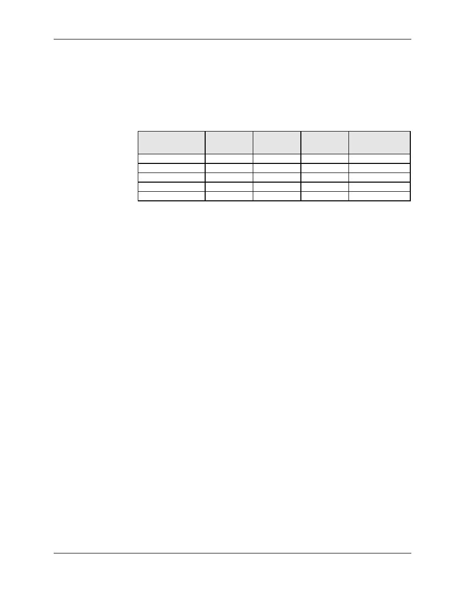
CX82100 Home Network Processor Data Sheet
12-2
Conexant Proprietary and Confidential Information
101306C
12.3
Timer Usage/SDRAM Refresh with Other Frequencies
Normal HNP operation assumes BCLK is 25, 50, 62.5, 75, or 100 MHz (see Section
13.1). The timer resolution circuitry and SDRAM refresh rates are based upon these
frequencies. However, if a different frequency is desired, the resolution of the timer and
SDRAM refresh rates are based on parameter values listed in Table 12-1.
Table 12-1. Timer Resolution and SDRAM Refresh Rate
BCLK Speed Select
(PLL_B_CR_SLOW)
EPCLK Clock
Rate Select
(PLL_B_CR)
Resolution
SDRAM
Refresh Rate
Notes
0 (Normal)
00 (
˜ 3)
PCLK/37.5
BCLK/900
0 (Normal)
01 (
˜ 4)
PCLK/50
BCLK/1200
0 (Normal)
10 (
˜ 5)
PCLK/62.5
BCLK/1500
1 (Slow)
00 (
˜ 1)
PCLK/12.5
BCLK/300
Default at POR
1 (Slow)
01 (
˜ 2)
PCLK/25
BCLK/600
SDRAMs typically require refresh rates at approximately 15.6
µs or faster. Normal HNP
operation, when configuring BCLK as in Section 13.1, achieves a refresh rate of 12
µs.
Care must be taken to avoid use of a refresh rate that is too slow. If the refresh rate is too
fast, application performance could be reduced.
A normal example is that BCLK is programmed for 100 MHz, with PLL_B_CR_SLOW
= 0 and PLL_B_CR = 01. PCLK would then be 50 MHz, EPCLK would then be 25
MHz, and the timer resolution would be 50/50 MHz, which is equal to 1
µs. The SDRAM
refresh rate would be 100 MHz/1200, which is equal to 12
µs.
An example using a different BCLK frequency is BCLK programmed to be 80 MHz,
with PLL_B_CR_SLOW = 0 and PLL_B_CR = 01. PCLK would then be 40 MHz,
EPCLK would then be 20 MHz, and the timer resolution would be 40 MHz/50, which is
equal to 1.25
µs. The SDRAM refresh rate would be 80 MHz/1200, which is equal to
15
µs.
Another example using a different BCLK frequency is BCLK programmed to be 40
MHz, with PLL_B_CR_SLOW = 1 (default) and PLL_B_CR = 00 (default). PCLK
would then be 20 MHz, EPCLK would then be 40 MHz, and the timer resolution would
be 20 MHz/12.5 which is equal to 0.625
µs. The SDRAM refresh rate would be 40
MHz/300, which is equal to 7.5
µs.
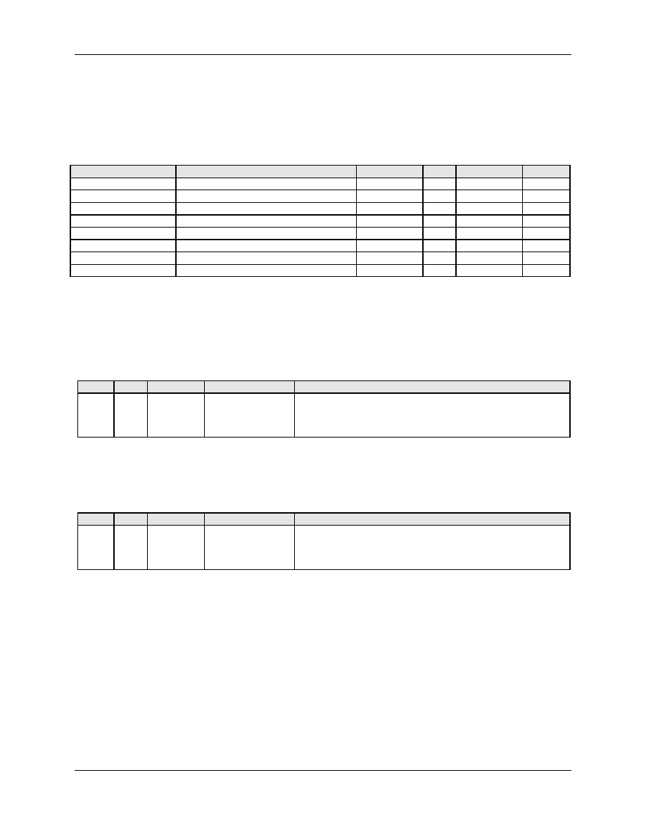
CX82100 Home Network Processor Data Sheet
101306C
Conexant Proprietary and Confidential Information
12-3
12.4
Timer Registers Memory Map
Timer registers are identified in Table 12-2.
Table 12-2. Timer Registers
Register Label
Register Name
ASB Address
Type
Default Value
Ref.
TM_Cnt1
Timer 1 Counter Register
0x00350020
RW
0x00000000
12.5.1
TM_Cnt2
Timer 2 Counter Register
0x00350024
RW
0x00000000
12.5.2
TM_Cnt3
Timer 3 Counter Register
0x00350028
RW
0x00000000
12.5.3
TM_Cnt4
Timer 4 Counter Register
0x0035002C
RW
0x00000000
12.5.4
TM_Lmt1
Timer 1 Limit Register
0x00350030
RW
0x00000000
12.5.5
TM_Lmt2
Timer 2 Limit Register
0x00350034
RW
0x00000000
12.5.6
TM_Lmt3
Timer 3 Limit Register
0x00350038
RW
0x00000000
12.5.7
TM_Lmt4
Timer 4 Limit Register
0x0035003C
RW
0x00000000
12.5.8
12.5
Timer Registers
12.5.1
Timer 1 Counter Register (TM_Cnt1: 0x00350020)
Bit(s)
Type
Default
Name
Description
15:0
RO
16'b0
TM_Cnt1
Timer 1 Current Counter Value.
Timer 1 increments every 1
µs, from 0 to the Timer 1 limit value, then
resets to 0 and counts again. TM_Cnt1 is reset whenever TM_Lmt1 is
written.
12.5.2
Timer 2 Counter Register (TM_Cnt2: 0x00350024)
Bit(s)
Type
Default
Name
Description
15:0
RO
16'b0
TM_Cnt2
Timer 2 Current Counter Value.
Timer 2 increments every 1
µs, from 0 to the Timer 2 limit value, then
resets to 0 and counts again. TM_Cnt2 is reset whenever TM_Lmt2 is
written.

CX82100 Home Network Processor Data Sheet
12-4
Conexant Proprietary and Confidential Information
101306C
12.5.3
Timer 3 Counter Register (TM_Cnt3: 0x00350028)
Bit(s)
Type
Default
Name
Description
15:0
RO
16'b0
TM_Cnt3
Timer 3 Current Counter Value.
Timer 3 increments every 1
µs, from 0 to the Timer 3 limit value, then
resets to 0 and counts again. TM_Cnt3 is reset whenever TM_Lmt3 is
written.
Timer 3 can be used as a Watchdog Timer (see Section 12.2).
12.5.4
Timer 4 Counter Register (TM_Cnt4: 0x0035002C)
Bit(s)
Type
Default
Name
Description
15:0
RO
16'b0
TM_Cnt4
Timer 4 Current Counter Value.
Timer 4 increments every 1
µs, from 0 to the Timer 4 limit value, then
resets to 0 and counts again. TM_Cnt4 is reset whenever TM_Lmt4 is
written.
12.5.5
Timer 1 Limit Register (TM_Lmt1: 0x00350030)
Bit(s)
Type
Default
Name
Description
15:0
RW
16'b0
TM_Lmt1
Timer 1 Limit Value.
When the Timer 1 current count reaches this limit value, the
Int_TIMER1 interrupt bit in the Interrupt Status Register (INT_Stat) is
set. The periodic timer interrupt event rate is = 1 MHz / (TM_Lmt1 +
1). If TM_Lmt1 is set to 0, TM_Cnt1 remains reset. TM_Cnt1 is reset
whenever TM_Lmt1 is written.
12.5.6
Timer 2 Limit Register (TM_Lmt2: 0x00350034)
Bit(s)
Type
Default
Name
Description
15:0
RW
16'b0
TM_Lmt2
Timer 2 Limit Value.
When the Timer 2 current count reaches this limit value, the
Int_TIMER2 interrupt bit in the Interrupt Status Register (INT_Stat) is
set. The periodic timer interrupt event rate is = 1 MHz / (TM_Lmt2 +
1). If TM_Lmt2 is set to 0, TM_Cnt2 remains reset. TM_Cnt2 is reset
whenever TM_Lmt2 is written.

CX82100 Home Network Processor Data Sheet
101306C
Conexant Proprietary and Confidential Information
12-5
12.5.7
Timer 3 Limit Register (TM_Lmt3: 0x00350038)
Bit(s)
Type
Default
Name
Description
15:0
RW
16'b0
TM_Lmt3
Timer 3 Limit Value.
When the Timer 3 current count reaches this limit value, the
Int_TIMER3 interrupt bit in the Interrupt Status Register (INT_Stat) is
set. The periodic timer interrupt event rate is = 1 MHz / (TM_Lmt3 +
1). If TM_Lmt3 is set to 0, TM_Cnt3 remains reset. TM_Cnt3 is reset
whenever TM_Lmt3 is written.
If 1'hF is written to the lower nibble, Watchdog Timer Mode is enabled
(see Section 12.2).
12.5.8
Timer 4 Limit Register (TM_Lmt4: 0x0035003C)
Bit(s)
Type
Default
Name
Description
15:0
RW
16'b0
TM_Lmt4
Timer 4 Limit Value.
When the Timer 4 current count reaches this limit value, the
Int_TIMER4 interrupt bit in the Interrupt Status Register (INT_Stat) is
set. The periodic timer interrupt event rate is = 1 MHz / (TM_Lmt4 +
1). If TM_Lmt4 is set to 0, TM_Cnt4 remains reset. TM_Cnt4 is reset
whenever TM_Lmt4 is written.

CX82100 Home Network Processor Data Sheet
12-6
Conexant Proprietary and Confidential Information
101306C
This page is intentionally blank.
CX82100 Home Network Processor Data Sheet
101306C
Conexant Proprietary and Confidential Information
13-1
13
Clock Generation Interface Description
The Clock Generation (CLKGEN) block generates internal and external clocks using two
programmable, fractional multiply phase locked loop (PLL) blocks, FCLK_PLL and
BCLK_PLL (Figure 13-1).
Included in each block is the actual PLL circuit with a voltage-controlled oscillator
(VCO) and post-PLL generation logic which divides the output of each PLL to create a
series of sub-multiple clocks.
Clock generation operation is controlled by the PLL Bypass (PLLBP) input pin and by
three registers: FCLK PLL Register (PLL_F), BCLK PLL Register (PLL_B), and Low
Power Mode Register (LPMR).
PLLBP input low selects PLL Normal Mode (see Section 13.1) and PLLBP input high
selects PLL Bypass Mode for factory clock test operation (see Section 13.7).
The signals on the FCLKIO/GPIO39 and BCLKIO/GPIO38 pins are also controlled by
the PLLBP pin and by the GPIO_Sel7 and GPIO_Sel6 control bits in the GPIO Optional
Register (GPIO_OPT, see Section 9.3.1), respectively. FCLKIO/GPIO39 pin control is
summarized in Table 13-1 and BCLKIO/GPIO38 pin control is summarized in Table
13-2.
When in PLL Bypass Mode, the FCLKIO and BCLKIO pins are configured as inputs,
and are divided and used in place of the PLL outputs. When in PLL Normal Mode, the
FCLKIO and BCLKIO pins can be configured as outputs, and provide a means to
indirectly observe the frequency of the internal clocks generated by the PLLs.
Table 13-1. FCLKIO/GPIO39 Pin Usage Control
PLLBP Input
Pin Voltage
Level
GPIO_Sel7 Bit in
GPIO Option Register (GPIO_OPT)
Signal on
FCLKIO/GPIO39 Pin
Pin Signal
Direction
Low
0
GPIO391
I/O
Low
1
UCLK2
O
High
Don't care
XFCLK2
I
Notes:
1. Default at power up reset.
2. See Figure 13-1.
Table 13-2. BCLKIO/GPIO38 Pin Usage Control
PLLBP Input
Pin Voltage
Level
GPIO_Sel6 Bit in
GPIO Option Register (GPIO_OPT)
Signal on
BCLKIO/GPIO38 Pin
Pin Signal
Direction
Low
0
GPIO381
I/O
Low
1
EPCLK2
O
High
Don't care
XBCLK2
I
Notes:
1. Default at power up reset.
2. See Figure 13-1.
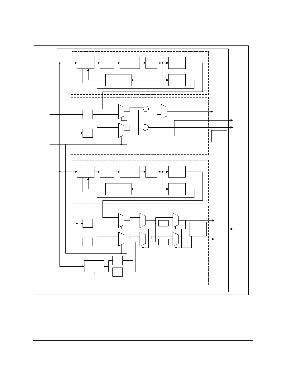
CX82100 Home Network Processor Data Sheet
13-2
Conexant Proprietary and Confidential Information
101306C
Figure 13-1. Clock Generation Block Diagram
PLL FCLK
FCLK PLL
PLL FCLK
PLL UCLK
(PLL FCLK/2)
Low Power
Mode Enable
(LPM_EN)
XFCLK
on FCLKIO
PLL Bypass Mode
(PLL_BP Pin
FCLK Slow
Speed Select
(PLL_F_CR_SLOW )
FCLK
UCLK
FCLK Generation Logic (Post FCLK PLL)
UCLK
on FCLKIO
Pre-Scaler
Divide by
3, 4, or 5
Phase
Detector
Charge Pump
and Loop Filter
VCO
Phase Detector
Divide by M.N
Output
Divider
(Divide by 2)
Output
Divider
(Divide by 4)
101545_064
Divide
by 2
Divide
by 4
0
1
0
1
0
1
PLL_F Prescale Select
(PLL_F_PRE)
PLL FCLK/2
PLL_BP
USB
Interface
(12 MHz)
HL_CLK
USB Clock
Rate Indicate
(PLL_F_CR)
PLL BCLK
BCLK PLL
PLL BCLK
PLL PCLK
(PLL BCLK/2)
Low Power
Mode Enable
(LPM_EN)
PLL Bypass Mode
(PLL_BP Pin
BCLK Generation Logic (Post BCLK PLL)
Pre-Scaler
Divide by
3, 4, or 5
Phase
Detector
Charge Pump
and Loop Filter
VCO
Phase Detector
Divide by M.N
Output
Divider
(Divide by 2)
Output
Divider
(Divide by 4)
Divide
by 2
Divide
by 4
0
1
0
1
PLL_B Prescale Select
(PLL_B_PRE)
PLL BCLK/2
0
1
0
1
0
1
0
1
Divide
by 2
Divide
by 4
BCLK Slow
Speed Select
(PLL_B_CR_SLOW )
Low Power
Mode Clock
Divider
XBCLK
on BCLKIO
Low Power
Mode Clock Divider
(LPM_CLK_DIV)
Divide
by 4
Divide
by 2
BCLK
PCLK
EPCLK
Divider
(by 3, 4, or 5
or 1 or 2)
EPCLK
on BCLKIO
EPCLK Clock
Rate Select
(PLL_B_CR)
CX82110 HNP
CLKI
XFCLK/2
XFCLK/4
XBCLK/2
XBCLK/4

CX82100 Home Network Processor Data Sheet
101306C
Conexant Proprietary and Confidential Information
13-3
13.1
PLL Normal Mode
When input pin PLLBP is low, the PLL output clocks are generated based on an
externally provided reference clock frequency on the CLKI pin, typically sourced from
an external oscillator. The CLKI frequency can range from 20 MHz to 40 MHz, 50%
duty cycle.
FCLK_PLL creates a family of frequencies related to 12 MHz. FCLK_PLL is typically
programmed to output 96, 120 144, or 168 MHz. The FCLK output is used directly by
the ARM9TDMI Core when programmed to asynchronous or synchronous modes (see
ARM documents). FCLK is divided by 2 to create UCLK for use by the USB Interface.
UCLK is the clock reference for USB timing, which requires a multiple of 12 MHz, with
a minimum frequency of 48 MHz.
BCLK_PLL creates a family of frequencies related to 25 MHz. BCLK_PLL is typically
programmed to output 50, 75 or 100 MHz. The BCLK output is used directly as the ASB
bus clock. BCLK is divided by 2 to create PCLK for the APB bus, and EPCLK (25 MHz)
for use by a separate Ethernet PHY device.
FCLK_PLL and BCLK_PLL each employ an independently controlled M.N fractional
divider in its PLL feedback circuit in order to synthesize frequencies which are not
integer multiples of the reference clock on CLKI.
The HNP defaults its clocks to "slow mode", meaning both the BCLK and FCLK are
operating at a slower frequency than is used in typical applications. This facilitates lower
power consumption immediately following power-on-reset. Typical applications will
program the PLLs to output higher frequencies at an appropriate time, e.g., after USB
enumeration.
Pins FCLKIO and BCLKIO can be configured to output clocks FCLK and EPCLK,
respectively, through the GPIO Option register (Section 9.3.1). Both pins default to GPIO
inputs immediately following power-on-reset.
The FCLK_PLL and the BCLK_PLL are implemented using 16-bit delta sigma (
Â)
synthesizers. FCLK_PLL is programmed by writing to the appropriate bits in the PLL_F
Register (see Section 13.4.1) and BCLK_PLL is programmed by writing to the
appropriate bits in the PLL_B Register (see Section 13.4.2). PLL operation is also
controlled by the Low Power Mode Register (LPMR) (see Section 13.4.3).
13.2
Generated Clocks
The FCLK PLL and BCLK PLL generated clocks are described in Table 13-3 and Table
13-4, respectively.
FCLK PLL and BCLK PLL generated clock frequencies for various programming
options are listed in Table 13-5 and Table 13-6, respectively.
All clocks are substituted with the JTAG Test Clock (pin TCK) when the HNP is in
boundary scan or internal scan mode.
The ARM940T processor uses BCLK in place of FCLK when in FastBus mode, which is
the default mode immediately following power-on-reset.
CX82100 Home Network Processor Data Sheet
13-4
Conexant Proprietary and Confidential Information
101306C
Table 13-3. FCLK PLL Generated Clocks
Clock
Minimum
Frequency
(MHz)
Maximum
Operating
Frequency
(MHz)
Description
FCLK
96
168
ARM940T fast clock input, asynchronous to bus clock. Can have a lower minimum if
the USB interface is not used. Internal. FCLK must be equal to or greater than BCLK.
UCLK
48
84
USB timing reference; always one-half the frequency of FCLK. Must be a multiple of
12 MHz for proper USB operation. Internal. Optionally external, output on FCLKIO
pin.
UDC
12
12
USB timing reference. Must be 12 MHz for proper USB operation; UCLK divided by
number corresponding to PLL_F_CR. Internal.
Table 13-4. BCLK PLL Generated Clocks
Clock
Minimum
Frequency
(MHz)
Maximum
Operating
Frequency
(MHz)
Description
BCLK
25
100
ASB clock. Internal. Can have a lower minimum if EPCLK is not used for 25 MHz.
PCLK
12.5
50
APB clock; always one-half the frequency of BCLK and aligned to BCLK falling edge.
Internal.
EPCLK
25
25
Miscellaneous timing reference, e.g., Ethernet PHY. Optionally external; output on
BCLKIO pin. Can be different frequency for applications other than an Ethernet PHY
clock.
Table 13-5. FCLK PLL Generated Clocks Programming Examples
FCLK Speed Select
(PLL_F_CR_SLOW)
PLL_F
Frequency
FCLK (ARM)
Frequency
UCLK
Frequency
(FCLK/2)
USB Clock
Rate Select
(PLL_F_CR)
UDC Clock
Frequency
Notes
0 (Normal)
96 MHz
96 MHz
48 MHz
00 (
˜ 8)
12 MHz
0 (Normal)
120 MHz
120 MHz
60 MHz
01 (
˜ 10)
12 MHz
0 (Normal)
144 MHz
144 MHz
72 MHz
10 (
˜ 12)
12 MHz
0 (Normal)
168 MHz
168 MHz
84 MHz
10 (
˜ 14)
12 MHz
1 (Slow)
96 MHz
48 MHz
48 MHz
00 (
˜ 4)
12 MHz
Default at POR
1 (Slow)
120 MHz
60 MHz
60 MHz
01 (
˜ 5)
12 MHz
1 (Slow)
144 MHz
72 MHz
72 MHz
10 (
˜ 6)
12 MHz
1 (Slow)
168 MHz
84 MHz
84 MHz
10 (
˜ 7)
12 MHz
Table 13-6. BCLK PLL Generated Clocks Programming Examples
BCLK Speed Select
(PLL_F_CR_SLOW)
PLL_B
Frequency
BCLK (ASB)
Frequency
PCLK (APB)
Frequency
(BCLK/2)
EPCLK Clock
Rate Select
(PLL_B_CR)
EPCLK
(XBCLK)
Clock
Frequency
Notes
0 (Normal)
75 MHz
75 MHz
37.5 MHz
00 (
˜ 3)
25 MHz
0 (Normal)
100 MHz
100 MHz
50 MHz
01 (
˜ 4)
25 MHz
1 (Slow)
50 MHz
25 MHz
12.5MHz
00 (
˜ 1)
25 MHz
Default at POR
1 (Slow)
100 MHz
50 MHz
25 MHz
01 (
˜ 2)
25 MHz

CX82100 Home Network Processor Data Sheet
101306C
Conexant Proprietary and Confidential Information
13-5
13.3
PLL Register Memory Map
Table 13-7. PLL Register Memory Map
Register Label
Register Name
ASB Address
Type
Default Value
Ref.
PLL_F
FCLK PLL Register
0x00350068
RW
0x18D04DEA
13.4.1
PLL_B
BCLK PLL Register
0x0035006C
RW
0x184E2730
13.4.2
LPMR
Low Power Mode Register
0x00350014
RW
0x00000000
13.4.3
13.4
PLL Registers
13.4.1
FCLK PLL Register (PLL_F: 0x00350068)
PLL_F register is used by the FCLK PLL to generated the desired FCLK/UCLK.
Bit(s)
Type
Default
Name
Description
31:29
Reserved.
28
RW
1'b1
PLL_F_CR_SLOW
FCLK Slow Speed Select.
0 = Normal FCLK speed.
1 = Slow FCLK speed (one-half normal speed), FCLK = UCLK.
(Default)
27
RO
1'b1
PLL_F_LK
FCLK PLL Lock Status.
0 = FCLK PLL not locked.
1 = FCLK PLL locked (must be continuous 1 to indicate proper
FCLK PLL operation).
26
RW
1'b0
PLL_F_DDS
Disable FCLK
Synthesizer.
0 = Enable FCLK
synthesizer and select fractional divides.
(Default)
1 = Disable the FCLK
synthesizer and select integer-only
divides.
25:24
RW
2'b00
PLL_F_CR
USB Clock Rate Indicate.
These bits indicate to the USB interface block the rate of UCLK. For
proper USB operation, UCLK should be programmed to 48, 60, 72, or
84 MHz.
00 =
UCLK rate is 48 MHz. (Default)
01 =
UCLK rate is 60 MHz.
10 =
UCLK rate is 72 MHz.
11 =
UCLK rate is 84 MHz.
23:22
RW
2'b11
PLL_F_PRE
FCLK Reference Input Prescale Divider Select.
00 =
Reserved.
01 =
Divide by 5. (Default)
10 =
Divide by 4.
11 =
Divide by 3.
21:16
RW
6'b010110
(22d)
PLL_F_INT
FCLK 6-bit Integer Divide Select.
0 =
Selects PLL power-down state.
14d Enables the PLL for normal operation as a clock synthesizer.
See 13.5. (Default)
15:0
RW
16'h4DEA
(19946d)
PLL_F_FRAC
FCLK 16-bit Fractional Divide.
See 13.5.

CX82100 Home Network Processor Data Sheet
13-6
Conexant Proprietary and Confidential Information
101306C
13.4.2
BCLK PLL Register (PLL_B: 0x0035006C)
PLL_B register is used by the BCLK PLL to generated the desired clocks
BCLK/PCLK/EPCLK.
Bit(s)
Type
Default
Name
Description
31:29
Reserved.
28
RW
1'b1
PLL_B_CR_SLOW
BCLK Slow Speed Select.
0 = Normal BCLK speed.
1 = Slow BCLK speed (one-half normal speed). (Default)
27
RO
1'b1
PLL_B_LK
BCLK PLL Lock Status.
0 = BCLK PLL not locked.
1 = BCLK PLL locked (must be continuous 1 to indicate proper
BCLK PLL operation).
26
RW
1'b0
PLL_B_DDS
Disable BCLK
Synthesizer.
0 = Enable BCLK
synthesizer and select fractional divides.
(Default)
1 = Disable the BCLK
synthesizer and select integer-only
divides.
25:24
RW
2'b00
PLL_B_CR
EPCLK Clock Rate Select Divider.
For PLL_B_CR_SLOW = 0:
00 =
BCLK divided by 3.
01 =
BCLK divided by 4.
10 =
BCLK divided by 5.
For PLL_B_CR_SLOW = 1:
00 =
BCLK divided by 1. (Default)
01 =
BCLK divided by 2.
10 =
Reserved.
23:22
RW
2'b01
PLL_B_PRE
BCLK Reference Input Prescale Divider Select.
00 =
Reserved.
01 =
Divide by 5. (Default)
10 =
Divide by 4.
11 =
Divide by 3.
21:16
RW
6'b001110
(14d)
PLL_B_INT
BCLK 6-bit Integer Divide Select.
0 =
Selects PLL power-down state.
14d Enables the PLL for normal operation as a clock synthesizer.
See 13.5. (Default)
15:0
RW
16'h2730
(10032d)
PLL_B_FRAC
BCLK 16-bit Fractional Divide.
See 13.5.

CX82100 Home Network Processor Data Sheet
101306C
Conexant Proprietary and Confidential Information
13-7
13.4.3
Low Power Mode Register (LPMR: 0x00350014)
Bit(s)
Type
Default
Name
Description
31:16
RW
16'b0
LPM_CLK_DIV
Low Power Mode Clock Divider.
In Low Power Mode, BCLK operation is changed to:
BCLK = CLKI/(LPM_CLK_DIV + 1)*2
For example, a BCLK as slow as 270 Hz can be generated using a
35.328 MHz CLKI as the input if Low Power Mode is enabled
(LPM_EN = 1) and BCLK slow speed is not selected
(PLL_B_CR_SLOW = 0 in the PLL_B register).
If both LPM_EN and PLL_B_CR_SLOW = 1, the clock frequency for
BCLK is additionally divided by 2.
15:1
Reserved.
0
RW
0
LPM_EN
Low Power Mode Enable.
0 = Normal mode.
1 = Enable Low Power Mode, i.e., BCLK operates as described in
LPMR[31:16]. It also switches off FCLK and UCLK to the
ARM40T Core and USB Block.
Note:
This control bit will not switch off or power-down the PLLs. To
put the PLLs in a power-down state, the PLL_F_INT / PLL_B_INT
values (bits [21:16] in PLL_F and PLL_B registers) must be 0.
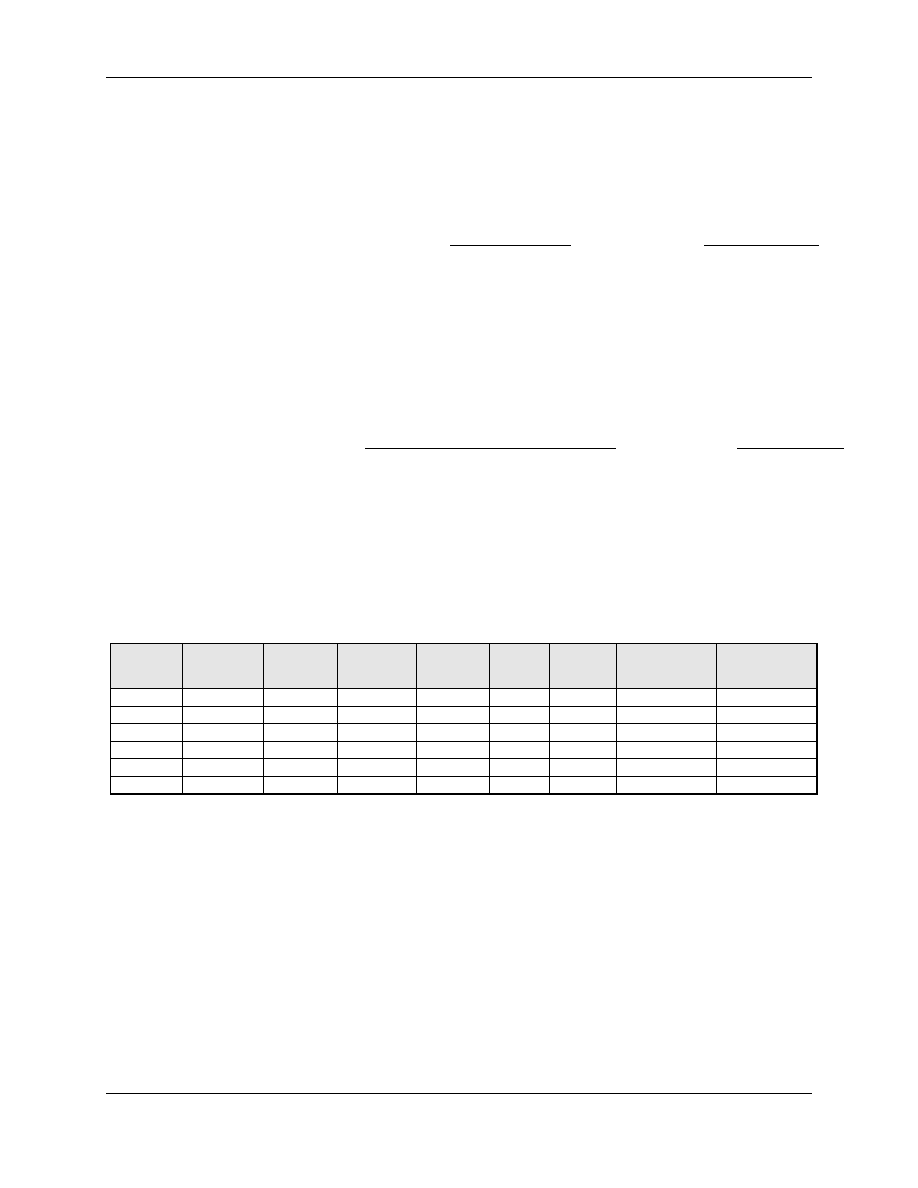
CX82100 Home Network Processor Data Sheet
13-8
Conexant Proprietary and Confidential Information
101306C
13.5
PLL Programming
The PLL output frequency synthesized is equal to:
(
)
2
2
_
}
_{
_
}
_{
_
}
_{
)
(
_
_
_
16
˜
˜
˜
¯
ˆ
Á
Á
Ë
Ê
+
◊
=
FRAC
X
PLL
INT
X
PLL
PRE
X
PLL
MHz
Freq
CLKI
MHz
Freq
Output
PLL
where X refers to F or B for the FCLK and BCLK PLLs, respectively.
For proper operation, FCLK must always be equal or greater than BCLK.
The divide ratio for each desired clock frequency is given by:
(
)
2
_
}
_{
_
}
_{
)
(
_
_
}
_{
2
_
_
16
FRAC
X
PLL
INT
X
PLL
MHz
Freq
CLKI
PRE
X
PLL
MHz
Freq
Desired
Ratio
Divide
+
=
◊
◊
=
At power-up and reset, both FCLK and BCLK and default to 48 MHz and 25 MHz,
respectively, when using a 35.328 MHz CLKI input.
Table 13-8 shows some desired frequencies and the necessary parameters for
programming the PLL_F and the PLL_B registers (assuming a 35.328 MHz input at
CLKI.
Table 13-8. Desired Frequencies and Programming Parameters
Example
CLKI
Frequency
(MHz)
PreScaler
Desired
Frequency
(MHz)
Divide
Ratio
Integer
(Dec.)
Fraction
(Dec.)
PLL Output
Frequency
(MHz)
PLL_Register
1
35.328
5
75
21.229620
21
15048
74.99998125
0x00553AC8
2
35.328
3
96
16.304348
16
19946
96.00002344
0x00D04DEA
3
35.328
4
100
22.644928
22
42266
100.000002
0x0196A51A
4
35.328
3
120
20.380435
20
24932
119.9999844
0x01D46164
5
35.328
3
144
24.456522
24
29919
144.0000352
0x02D874DF
6
35.328
3
168
28.532608
28
34905
167.9999960
0x03DC8859
CX82100 Home Network Processor Data Sheet
101306C
Conexant Proprietary and Confidential Information
13-9
13.6
Watchdog Timer Mode
When Timer 3 is in Watchdog Timer Mode (see Section 12.2), the PLL registers are
disabled from updates by APB writes. This guarantees uninterrupted clocking in the
event a Watchdog Timer timeout and subsequent system reset occurs. There is, however,
a time window when the PLLs can be updated. This occurs when the 7-bit counter that
counts to 100 (incremented every Int_TM3) is equal to 0 or 1. Since this counter is
cleared every time the TM_Lmt3 is written, the time window for allowed PLL updates is
usually open. When the ARM program is not running properly, the window will close,
eventually cause a system reset.
13.7
PLL Bypass Mode
If PLLBP is set high, the PLLs are bypassed and the HNP is in test-clock mode with
clocks supplied from the FCLKIO and BCLKIO pins (Figure 13-1). The clock provided
by FCLKIO is called XFCK and the clock provided by BCLKIO is called XBCK. The
clocking requirement is shown in Table 13-9.
Table 13-9. Clocking Requirements
Clock
Maximum
Frequency (MHz)
Accuracy
(ppm)
Duty Cycle
(%)
Description
XFCK
144
100
50
± 2
ARM940T fast clock input
XBCK
100
100
50
± 2
ASB clock
In order to setup the test clock mode, configuration control bits must be loaded by pulsing
the CLKI pin. The rising edge of CLKI saves the state of XFCK and XBCK into a control
register (XBCTL, XFCTL) internal to the PLL hardware (and not visible to the software).
The clock used to bypass the VCO in PLL_B is created by the XOR (XBCK, XFCK, and
XBCTL). The clock used to bypass the VCO in PLL_F is created by the XOR (XFCK,
XBCK, and XFCTL). Thus the two PLLs can be bypassed with independent clocks, but
at only Ω the maximum possible frequency, when the control bits are reset to zero. An
internal test VCO bypass clock can be generated at twice the frequency of the external
pin clocks if the XBCK and XFCK are signaled in quadrature (90 degrees out of phase),
and the appropriate control bit(s) is (are) activated (see Figure 13-2).
Note that CLKI also serves as an active-high asynchronous reset for the PLL post-
dividers when PLLBP is high, otherwise the POR is used. The internal bus clocks will
not progress until CLKI is reset low while in test-clock mode.
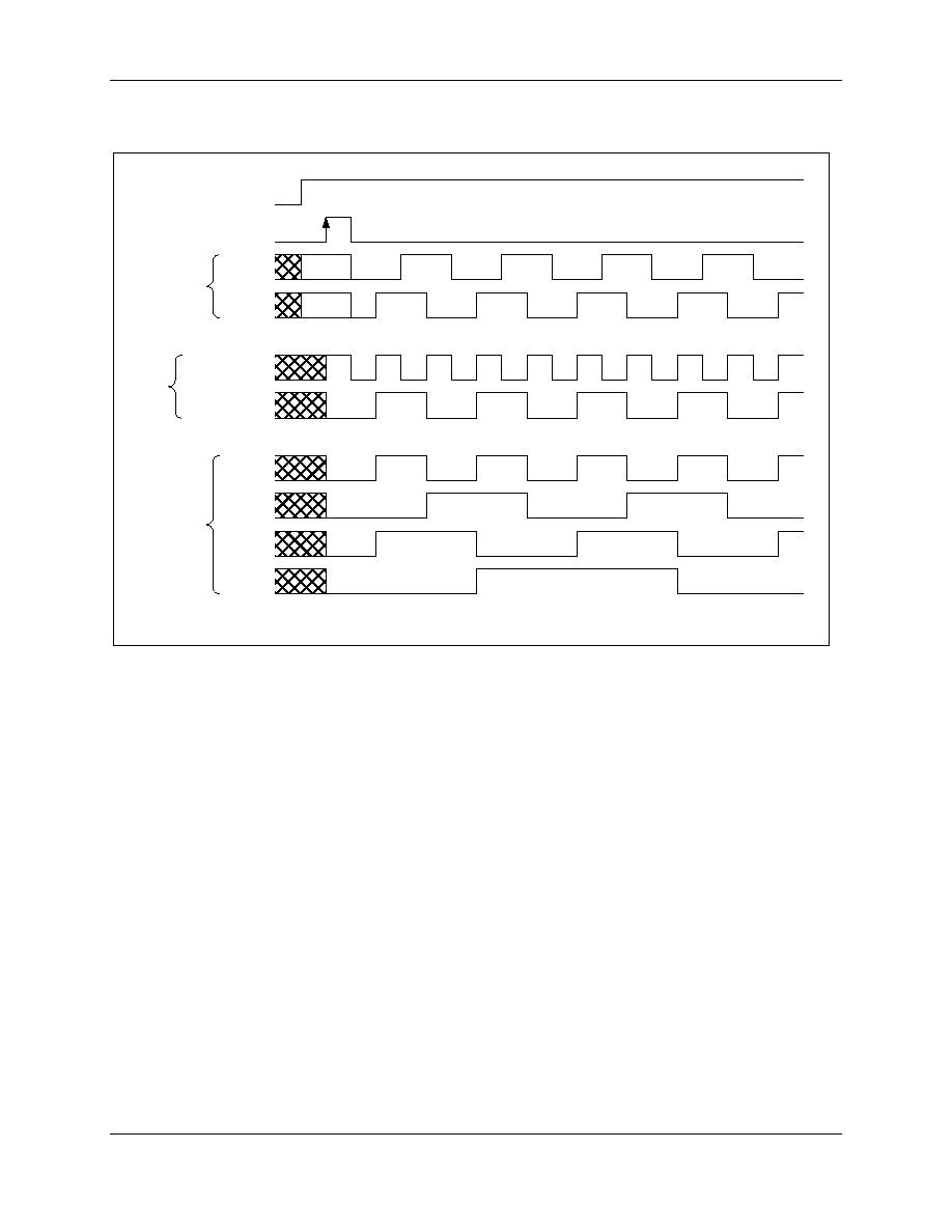
CX82100 Home Network Processor Data Sheet
13-10
Conexant Proprietary and Confidential Information
101306C
Figure 13-2. Clocks Generated in the PLL Bypass Mode
101545_063
PLLBP
BCLK
PCLK
rst
CLKI
XBCTL=0
XBCK
XFCK
XFCTL=1
VCO Bypass
Clock in PLL_B
FCLK
UCLK
VCO Bypass
Clock in PLL_F
Input
Clocks
Internal
Clocks
Output
Clocks
Note: This figure assum es PLL_X_CR_SLOW = 0.
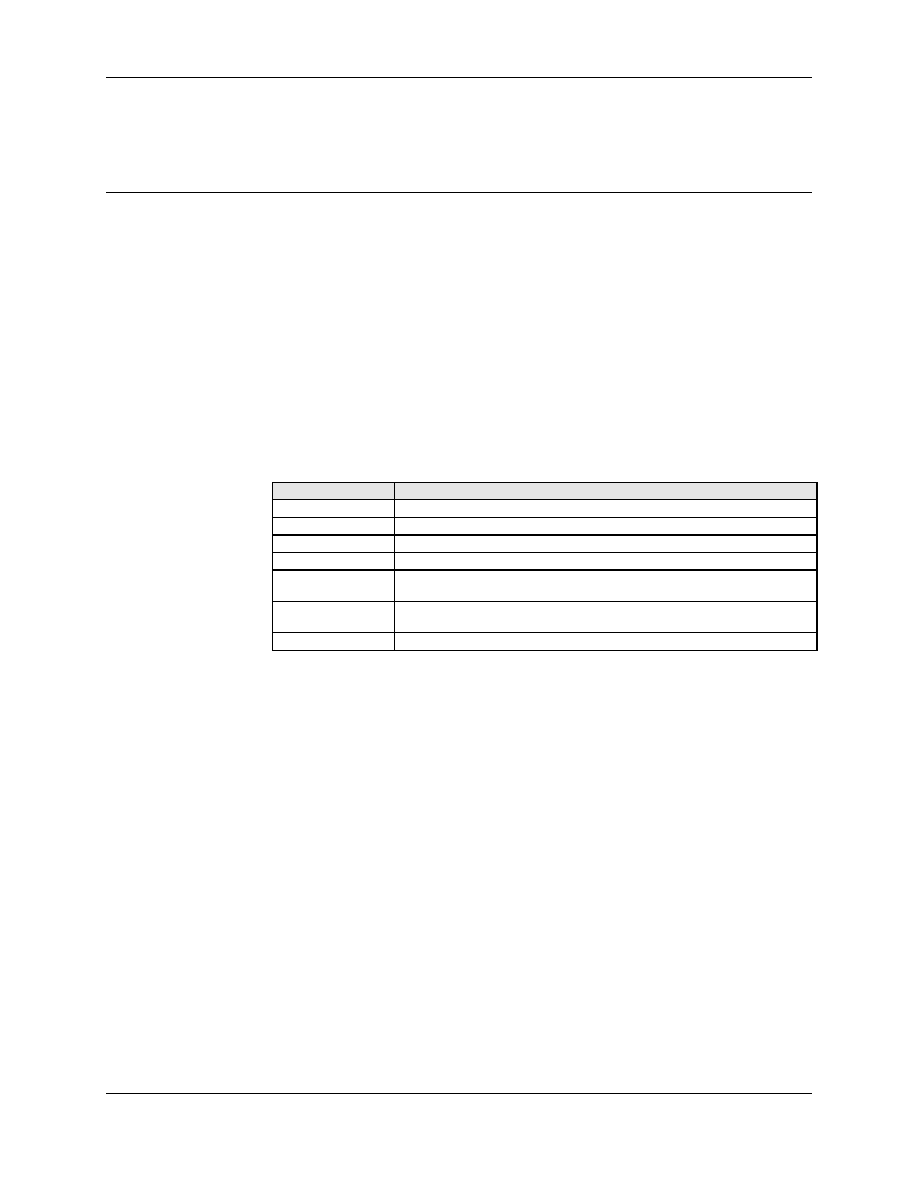
CX82100 Home Network Processor Data Sheet
101306C
Conexant Proprietary and Confidential Information
14-1
14
Register Map Summary
Most of the register set resides on the APB. These registers are accessible by the
microcontroller directly (memory-mapped). They are also accessible by the host slave-
mode interface indirectly (host pointer).
14.1
Register Type Definition
The register types are defined in Table 14-1.
All registers are not pre-fetchable, which would imply side effects from reads. This
means that read or write accesses, sequential or not, may drive state-dependent state
control.
Table 14-1. Register Type Definition
Register Type
Description
RO
Read-only
WO
Write-only
RW
Read / Write
RW*
Read / Write, but data may not be same as written at a later time.
RR
Same as RW, but writing a 1 resets corresponding bit location, writing 0 has
no effect.
RWp
Read-only, Write-only shared port, data written cannot be read. Only
accessible by DMAC
Wd
Write-only, operates on other data entering register.

CX82100 Home Network Processor Data Sheet
14-2
Conexant Proprietary and Confidential Information
101306C
14.2
Interface Registers Sorted by Supported Function
The CX82100 interface registers sorted by supported function are listed in Table 14-2.
Table 14-2. CX82100 Interface Registers Sorted by Supported Function
Register Label
Register Name
ASB Address
Type
Default Value
Ref.
DMAC Registers
DMAC_1_Ptr1
DMAC 1 Current Pointer 1
0x00300000
RW*
0x00000000
4.5.1
DMAC_2_Ptr1
DMAC 2 Current Pointer 1
0x00300004
RO
0x00000000
4.5.1
DMAC_3_Ptr1
DMAC 3 Current Pointer 1
0x00300008
RW*
0x00000000
4.5.1
DMAC_4_Ptr1
DMAC 4 Current Pointer 1
0x0030000C
RO
0x00000000
4.5.1
DMAC_5_Ptr1
DMAC 5 Current Pointer 1
0x00300010
RW*
0x00000000
4.5.1
DMAC_6_Ptr1
DMAC 6 Current Pointer 1
0x00300014
RW*
0x00000000
4.5.1
DMAC_7_Ptr1
DMAC 7 Current Pointer 1
0x00300018
RW*
0x00000000
4.5.1
DMAC_8_Ptr1
DMAC 8 Current Pointer 1
0x0030001C
RW*
0x00000000
4.5.1
DMAC_9_Ptr1
DMAC 9 Current Pointer 1
0x00300020
RW*
0x00000000
4.5.1
DMAC_10_Ptr1
DMAC 10 Current Pointer 1
0x00300024
RW*
0x00000000
4.5.1
DMAC_11_Ptr1
DMAC 11 Current Pointer 1
0x00300028
RW*
0x00000000
4.5.1
*** Reserved ***
0x0030002C
DMAC_1_Ptr2
DMAC 1 Indirect/Return Pointer 2
0x00300030
RW*
0x00000000
4.5.4
DMAC_2_Ptr2
DMAC 2 Indirect/Return Pointer 2
0x00300034
RW*
0x00000000
4.5.4
DMAC_3_Ptr2
DMAC 3 Indirect/Return Pointer 2
0x00300038
RW*
0x00000000
4.5.4
DMAC_4_Ptr2
DMAC 4 Indirect/Return Pointer 2
0x0030003C
RW*
0x00000000
4.5.4
DMAC_5_Ptr2
DMAC 5 Indirect/Return Pointer 2
0x00300040
RW*
0x00000000
4.5.4
*** Reserved ***
0x00300044≠
0x0030005C
DMAC_1_Cnt1
DMAC 1 Buffer Size Counter 1
0x00300060
RW*
0x00000000
4.5.3
DMAC_2_Cnt1
DMAC 2 Buffer Size Counter 1
0x00300064
RW*
0x00000000
4.5.3
DMAC_3_Cnt1
DMAC 3 Buffer Size Counter 1
0x00300068
RW*
0x00000000
4.5.3
DMAC_4_Cnt1
DMAC 4 Buffer Size Counter 1
0x0030006C
RW*
0x00000000
4.5.3
DMAC_5_Cnt1
DMAC 5 Buffer Size Counter 1
0x00300070
RW*
0x00000000
4.5.3
DMAC_6_Cnt1
DMAC 6 Buffer Size Counter 1
0x00300074
RW*
0x00000000
4.5.3
*** Reserved ***
0x00300078≠
0x0030007C
DMAC_9_Cnt1
DMAC 9 Buffer Size Counter 1
0x00300080
RW*
0x00000000
4.5.3
DMAC_10_Cnt1
DMAC 10 Buffer Size Counter 1
0x00300084
RW*
0x00000000
4.5.3
DMAC_11_Cnt1
DMAC 11 Buffer Size Counter 1
0x00300088
RW*
0x00000000
4.5.3
*** Reserved ***
0x0030008C≠
0x00300090
DMAC_2_Cnt2
DMAC 2 Buffer Size Counter 2
0x00300094
WO
0x00000000
4.5.4
*** Reserved ***
0x00300098
DMAC_4_Cnt2
DMAC 4 Buffer Size Counter 2
0x0030009C
WO
0x00000000
4.5.4
*** Reserved ***
0x003000A0≠
0x003000FC
DMAC_12_Ptr1
DMAC 11 Current Pointer 1
0x00300100
RW*
0x00000000
4.5.1
DMAC_13_Ptr1
DMAC 12 Current Pointer 1
0x00300104
RW*
0x00000000
4.5.1
*** Reserved ***
0x00300108≠
0x0030010C
DMAC_12_Cnt1
DMAC 11 Buffer Size Counter 1
0x00300110
RW*
0x00000000
4.5.3
DMAC_13_Cnt1
DMAC 12 Buffer Size Counter 1
0x00300114
RW*
0x00000000
4.5.3
*** Reserved ***
0x00300118≠
0x00300124

CX82100 Home Network Processor Data Sheet
101306C
Conexant Proprietary and Confidential Information
14-3
Table 16-2. CX82100 Interface Registers Sorted by Supported Function (Continued)
Register Label
Register Name
ASB Address
Type
Default Value
Ref.
Host Interface Registers
HST_CTRL
Host Control Register
0x002D0000
RW
0x00000008
5.3.1
HST_RWST
Host Master Mode Read-Wait-State Control
Register
0x002D0004
RW
0x00739CE7
5.3.2
HST_WWST
Host Master Mode Write-Wait-State Control
Register
0x002D0008
RW
0x00739CE7
5.3.3
HST_XFER_CNTL
Host Master Mode Transfer Control Register
0x002D000C
RW
0x00000000
5.3.4
HST_READ_CNTL1
Host Master Mode Read Control Register 1
0x002D0010
RW
0x00000000
5.3.5
HST_READ_CNTL2
Host Master Mode Read Control Register 2
0x002D0014
RW
0x00000000
5.3.6
HST_WRITE_CNTL1
Host Master Mode Write Control Register 1
0x002D0018
RW
0x00000000
5.3.7
HST_WRITE_CNTL2
Host Master Mode Write Control Register 2
0x002D001C
RW
0x00000000
5.3.8
MSTR_INTF_WIDTH
Host Master Mode Peripheral Size
0x002D0020
RW
0x00000000
5.3.9
MSTR_HANDSHAKE
Host Master Mode Peripheral Handshake
0x002D0024
RW
0x00000000
5.3.10
HDMA_SRC_ADDR
Host Master Mode DMA Source Address
0x002D0028
RW
0x00000000
5.3.11
HDMA_DST_ADDR
Host Master Mode DMA Destination Address
0x002D002C
RW
0x00000000
5.3.12
HDMA_BCNT
Host Master Mode DMA Byte Count
0x002D0030
RW
0x00000000
5.3.13
HDMA_TIMERS
Host Master Mode DMA Timers
0x002D0034
RW
0x00000000
5.3.14
External Memory Control Register
EMCR
External Memory Control Register
0x00350010
RW
0x00000000
6.12.1
EMAC Registers
E_DMA_1
EMAC 1 Source/Destination DMA Data Register
0x00310000
RWp
(don't care)
7.11.1
E_NA_1
EMAC 1 Network Access Register
0x00310004
RW
0x80200000
7.11.3
E_Stat_1
EMAC 1 Status Register
0x00310008
RW*
0x00000000
7.11.4
E_IE_1
EMAC 1 Interrupt Enable Register
0x0031000C
RW
0x00000000
7.11.6
E_LP_1
EMAC 1 Receiver Last Packet Register
0x00310010
RW*
0x00000000
7.11.5
E_MII_1
EMAC 1 MII Management Interface Register
0x00310018
RW1
0x00000008
7.11.7
ET_DMA_1
EMAC 1 Destination DMA Data Register
0x00310020
ROp
(don't care)
7.11.2
E_DMA_2
EMAC 2 Source/Destination DMA Data Register
0x00320000
RWp
(don't care)
7.11.1
E_NA_2
EMAC 2 Network Access Register
0x00320004
RW
0x80200000
7.11.3
E_Stat_2
EMAC 2 Status Register
0x00320008
RW*
0x00000000
7.11.4
E_IE_2
EMAC 2 Interrupt Enable Register
0x0032000C
RW
0x00000000
7.11.6
E_LP_2
EMAC 2 Receiver Last Packet Register
0x00320010
RW*
0x00000000
7.11.5
E_MII_2
EMAC 2 MII Management Interface Register
0x00320018
RW2
0x00000008
7.11.7
ET_DMA_2
EMAC 2 Destination DMA Data Register
0x00320020
ROp
(don't care)
7.11.2
USB Registers
U0_DMA
USB Source/Destination DMA Data Register 0
0x00330000
RWp
(don't care)
8.8.1
U1_DMA
USB Source/Destination DMA Data Register 1
0x00330008
RWp
(don't care)
8.8.2
U2_DMA
USB Source/Destination DMA Data Register 2
0x00330010
RWp
(don't care)
8.8.3
U3_DMA
USB Source/Destination DMA Data Register 3
0x00330018
RWp
(don't care)
8.8.4
UT_DMA
USB Destination DMA Data Register
0x00330020
RO
(don't care)
8.8.5
U_CFG
USB Configuration Data Register
0x00330024
RW
0x00000000
8.8.6
U_IDAT
USB Interrupt Data Register
0x00330028
RW
0x00000000
8.8.7
U_CTR1
USB Control Register 1
0x0033002C
RW
0x04000000
8.8.8
U_CTR2
USB Control Register 2
0x00330030
RW
0x00000000
8.8.9
U_CTR3
USB Control Register 3
0x00330034
RW
0x00000000
8.8.10
U_STAT
USB Status
0x00330038
RR
0x00000000
8.8.11
U_IER
USB Interrupt Enable Register
0x0033003C
RW
0x00000000
8.8.12
U_STAT2
USB Status Register 2
0x00330040
RR
0x00000000
8.8.13
U_IER2
USB Interrupt Enable Register 2
0x00330044
RW
0x00000000
8.8.14
EP0_IN_TX_INC
EP0_IN Transmit Increment Register
0x00330048
RW
0x00000000
8.9.1
EP0_IN_TX_PEND
EP0_IN Transmit Pending Register
0x0033004C
RO
0x00000000
8.9.2
EP0_IN_TX_QWCNT
EP0_IN Transmit qword Count Register
0x00330050
RO
0x00000000
8.9.3
1
Note: The bit E_MII_1[1] is Read Only.
2
Note: The bit E_MII_2[1] is Read Only.

CX82100 Home Network Processor Data Sheet
14-4
Conexant Proprietary and Confidential Information
101306C
Table 16-2. CX82100 Interface Registers Sorted by Supported Function (Continued)
Register Label
Register Name
ASB Address
Type
Default Value
Ref.
EP1_IN_TX_INC
EP1_IN Transmit Increment Register
0x00330054
RW
0x00000000
8.9.4
EP1_IN_TX_PEND
EP1_IN Transmit Pending Register
0x00330058
RO
0x00000000
8.9.5
EP1_IN_TX_QWCNT
EP1_IN Transmit qword Count Register
0x0033005C
RO
0x00000000
8.9.6
EP2_IN_TX_INC
EP2_IN Transmit Increment Register
0x00330060
RW
0x00000000
8.9.7
EP2_IN_TX_PEND
EP2_IN Transmit Pending Register
0x00330064
RO
0x00000000
8.9.8
EP2_IN_TX_QWCNT
EP2_IN Transmit qword Count Register
0x00330068
RO
0x00000000
8.9.9
EP3_IN_TX_INC
EP3_IN Transmit Increment Register
0x0033006C
RW
0x00000000
8.9.10
EP3_IN_TX_PEND
EP3_IN Transmit Pending Register
0x00330070
RO
0x00000000
8.9.11
EP3_IN_TX_QWCNT
EP3_IN Transmit qword Count Register
0x00330074
RO
0x00000000
8.9.12
EP_OUT_RX_DEC
EP_OUT Receive Decrement Register
0x00330078
RW
0x00000000
8.9.13
EP_OUT_RX_PEND
EP_OUT Receive Pending Register
0x0033007C
RO
0x00000000
8.9.14
EP_OUT_RX_QWCNT
EP_OUT Receive qword Count Register
0x00330080
RO
0x00000000
8.9.16
EP_OUT_RX_BUFSIZE
EP_OUT Receive Buffer Size Register
0x00330084
RW
0x00000000
8.9.15
U_CSR
USB Control-Status Register
0x00330088
RO/WO
0x00000000
8.9.20
UDC_TSR
UDC Time Stamp Register
0x0033008C
RO
0x00000000
8.8.15
UDC_STAT
UDC Status Register
0x00330090
RO
0x00000000
8.8.16
USB_RXTIMER
USB Receive DMA Watchdog Timer Register
0x00330094
RW
0x00000000
8.9.17
USB_RXTIMERCNT
USB Receive DMA Watchdog Timer Counter
Register
0x00330098
RO
0x00000000
8.9.18
EP_OUT_RX_PENDLEVEL
EP_OUT Receive Pending Interrupt Level Register
0x0033009C
RW
0x00000000
8.9.19
Timer Registers
TM_Cnt1
Timer 1 Counter Register
0x00350020
RW
0x00000000
12.5.1
TM_Cnt2
Timer 2 Counter Register
0x00350024
RW
0x00000000
12.5.2
TM_Cnt3
Timer 3 Counter Register
0x00350028
RW
0x00000000
12.5.3
TM_Cnt4
Timer 4 Counter Register
0x0035002C
RW
0x00000000
12.5.4
TM_Lmt1
Timer 1 Limit Register
0x00350030
RW
0x00000000
12.5.5
TM_Lmt2
Timer 1 Limit Register
0x00350034
RW
0x00000000
12.5.6
TM_Lmt3
Timer 1 Limit Register
0x00350038
RW
0x00000000
12.5.7
TM_Lmt4
Timer 1 Limit Register
0x0035003C
RW
0x00000000
12.5.8
GPIO Registers
GPIO_ISM1
GPIO Interrupt Sensitivity Mode Register 1
0x003500A0
RW
0x00000000
9.3.20
GPIO_ISM2
GPIO Interrupt Sensitivity Mode Register 2
0x003500A4
RW
0x00000000
9.3.21
GPIO_ISM3
GPIO Interrupt Sensitivity Mode Register 3
0x003500A8
RW
0x00000000
9.3.22
GPIO_OPT
GPIO Option Register
0x003500B0
RW
0x00000000
9.3.1
GPIO_OE1
GPIO Output Enable Register 1
0x003500B4
RW
0x00002306
9.3.2
GPIO_OE2
GPIO Output Enable Register 2
0x003500B8
RW
0x00000082
9.3.3
GPIO_OE3
GPIO Output Enable Register 3
0x003500BC
RW
0x00000000
9.3.4
GPIO_DATA_IN1
GPIO Data Input Register 1
0x003500C0
RO
0x00000000
9.3.5
GPIO_DATA_IN2
GPIO Data Input Register 2
0x003500C4
RO
0x00000000
9.3.6
GPIO_DATA_IN3
GPIO Data Input Register 3
0x003500C8
RO
0x00000000
9.3.7
GPIO_DATA_OUT1
GPIO Data Output Register 1
0x003500CC
RW
0x23062306
9.3.8
GPIO_DATA_OUT2
GPIO Data Output Register 2
0x003500D0
RW
0x00960086
9.3.9
GPIO_DATA_OUT3
GPIO Data Output Register 3
0x003500D4
RW
0x00000000
9.3.10
GPIO_ISR1
GPIO Interrupt Status Register 1
0x003500D8
RR
0x00000000
9.3.11
GPIO_ISR2
GPIO Interrupt Status Register 2
0x003500DC
RR
0x00000000
9.3.12
GPIO_ISR3
GPIO Interrupt Status Register 3
0x003500E0
RR
0x00000000
9.3.13
GPIO_IER1
GPIO Interrupt Enable Register 1
0x003500E4
RW
0x00000000
9.3.14
GPIO_IER2
GPIO Interrupt Enable Register 2
0x003500E8
RW
0x00000000
9.3.15
GPIO_IER3
GPIO Interrupt Enable Register 3
0x003500EC
RW
0x00000000
9.3.16
GPIO_IPC1
GPIO Interrupt Polarity Control Register 1
0x003500F0
RW
0x00000000
9.3.17
GPIO_IPC2
GPIO Interrupt Polarity Control Register 2
0x003500F4
RW
0x00000000
9.3.18
GPIO_IPC3
GPIO Interrupt Polarity Control Register 3
0x003500F8
RW
0x00000000
9.3.19
EMAC Register
M2M_DMA
Memory to Memory DMA Data Register
0x00350000
RWp
64'bx
10.3.1
M2M_Cntl
Memory to Memory DMA Transfer Control/Counter
0x00350004
RW
0x00000000
10.3.2
Interrupt Registers
INT_LA
Interrupt Level Assignment Register
0x00350040
RW
0x00000000
11.2.1
INT_Stat
Interrupt Status Register
0x00350044
RR
0x00000000
11.2.2

CX82100 Home Network Processor Data Sheet
101306C
Conexant Proprietary and Confidential Information
14-5
Register Label
Register Name
ASB Address
Type
Default Value
Ref.
INT_SetStat
Interrupt Set Status Register
0x00350048
WO
0x00000000
11.2.3
INT_Msk
Interrupt Mask Register
0x0035004C
RW
0x00000000
11.2.4
INT_Mstat
Interrupt Mask Status Register
0x00350090
RO
0x00000000
11.2.5
Low Power and PLL Registers
LPMR
Low Power Mode Register
0x00350014
RW
0x00000000
13.4.3
PLL_F
FCLK PLL Register
0x00350068
RW
0x18D04DEA
13.4.1
PLL_B
BCLK PLL Register
0x0035006C
RW
0x184E2730
13.4.2

CX82100 Home Network Processor Data Sheet
14-6
Conexant Proprietary and Confidential Information
101306C
14.3
Interface Registers Sorted by Address
The CX82100 interface registers sorted by address are listed in Table 14-3.
Table 14-3. CX82100 Interface Registers Sorted by Address
Register Label
Register Name
ASB Address
Type
Default Value
Ref.
HST_CTRL
Host Control Register
0x002D0000
RW
0x00000008
5.3.1
HST_RWST
Host Master Mode Read-Wait-State Control
Register
0x002D0004
RW
0x00739CE7
5.3.2
HST_WWST
Host Master Mode Write-Wait-State Control
Register
0x002D0008
RW
0x00739CE7
5.3.3
HST_XFER_CNTL
Host Master Mode Transfer Control Register
0x002D000C
RW
0x00000000
5.3.4
HST_READ_CNTL1
Host Master Mode Read Control Register 1
0x002D0010
RW
0x00000000
5.3.5
HST_READ_CNTL2
Host Master Mode Read Control Register 2
0x002D0014
RW
0x00000000
5.3.6
HST_WRITE_CNTL1
Host Master Mode Write Control Register 1
0x002D0018
RW
0x00000000
5.3.7
HST_WRITE_CNTL2
Host Master Mode Write Control Register 2
0x002D001C
RW
0x00000000
5.3.8
MSTR_INTF_WIDTH
Host Master Mode Peripheral Size
0x002D0020
RW
0x00000000
5.3.9
MSTR_HANDSHAKE
Host Master Mode Peripheral Handshake
0x002D0024
RW
0x00000000
5.3.10
HDMA_SRC_ADDR
Host Master Mode DMA Source Address
0x002D0028
RW
0x00000000
5.3.11
HDMA_DST_ADDR
Host Master Mode DMA Destination Address
0x002D002C
RW
0x00000000
5.3.12
HDMA_BCNT
Host Master Mode DMA Byte Count
0x002D0030
RW
0x00000000
5.3.13
HDMA_TIMERS
Host Master Mode DMA Timers
0x002D0034
RW
0x00000000
5.3.14
DMAC_1_Ptr1
DMAC 1 Current Pointer 1
0x00300000
RW*
0x00000000
4.5.1
DMAC_2_Ptr1
DMAC 2 Current Pointer 1
0x00300004
RO
0x00000000
4.5.1
DMAC_3_Ptr1
DMAC 3 Current Pointer 1
0x00300008
RW*
0x00000000
4.5.1
DMAC_4_Ptr1
DMAC 4 Current Pointer 1
0x0030000C
RO
0x00000000
4.5.1
DMAC_5_Ptr1
DMAC 5 Current Pointer 1
0x00300010
RW*
0x00000000
4.5.1
DMAC_6_Ptr1
DMAC 6 Current Pointer 1
0x00300014
RW*
0x00000000
4.5.1
DMAC_7_Ptr1
DMAC 7 Current Pointer 1
0x00300018
RW*
0x00000000
4.5.1
DMAC_8_Ptr1
DMAC 8 Current Pointer 1
0x0030001C
RW*
0x00000000
4.5.1
DMAC_9_Ptr1
DMAC 9 Current Pointer 1
0x00300020
RW*
0x00000000
4.5.1
DMAC_10_Ptr1
DMAC 10 Current Pointer 1
0x00300024
RW*
0x00000000
4.5.1
DMAC_11_Ptr1
DMAC 11 Current Pointer 1
0x00300028
RW*
0x00000000
4.5.1
*** Reserved ***
0x0030002C
DMAC_1_Ptr2
DMAC 1 Indirect/Return Pointer 2
0x00300030
RW*
0x00000000
4.5.4
DMAC_2_Ptr2
DMAC 2 Indirect/Return Pointer 2
0x00300034
RW*
0x00000000
4.5.4
DMAC_3_Ptr2
DMAC 3 Indirect/Return Pointer 2
0x00300038
RW*
0x00000000
4.5.4
DMAC_4_Ptr2
DMAC 4 Indirect/Return Pointer 2
0x0030003C
RW*
0x00000000
4.5.4
DMAC_5_Ptr2
DMAC 5 Indirect/Return Pointer 2
0x00300040
RW*
0x00000000
4.5.4
*** Reserved ***
0x00300044≠
0x0030005C
DMAC_1_Cnt1
DMAC 1 Buffer Size Counter 1
0x00300060
RW*
0x00000000
4.5.3
DMAC_2_Cnt1
DMAC 2 Buffer Size Counter 1
0x00300064
RW*
0x00000000
4.5.3
DMAC_3_Cnt1
DMAC 3 Buffer Size Counter 1
0x00300068
RW*
0x00000000
4.5.3
DMAC_4_Cnt1
DMAC 4 Buffer Size Counter 1
0x0030006C
RW*
0x00000000
4.5.3
DMAC_5_Cnt1
DMAC 5 Buffer Size Counter 1
0x00300070
RW*
0x00000000
4.5.3
DMAC_6_Cnt1
DMAC 6 Buffer Size Counter 1
0x00300074
RW*
0x00000000
4.5.3
*** Reserved ***
0x00300078≠
0x0030007C
DMAC_9_Cnt1
DMAC 9 Buffer Size Counter 1
0x00300080
RW*
0x00000000
4.5.3
DMAC_10_Cnt1
DMAC 10 Buffer Size Counter 1
0x00300084
RW*
0x00000000
4.5.3
DMAC_11_Cnt1
DMAC 11 Buffer Size Counter 1
0x00300088
RW*
0x00000000
4.5.3
*** Reserved ***
0x0030008C≠
0x00300090
DMAC_2_Cnt2
DMAC 2 Buffer Size Counter 2
0x00300094
WO
0x00000000
4.5.4
*** Reserved ***
0x00300098
DMAC_4_Cnt2
DMAC 4 Buffer Size Counter 2
0x0030009C
WO
0x00000000
4.5.4
*** Reserved ***
0x003000A0≠
0x003000FC

CX82100 Home Network Processor Data Sheet
101306C
Conexant Proprietary and Confidential Information
14-7
Table 16-3. CX82100 Interface Registers Sorted by Address (Continued)
Register Label
Register Name
ASB Address
Type
Default Value
Ref.
DMAC_12_Ptr1
DMAC 11 Current Pointer 1
0x00300100
RW*
0x00000000
4.5.1
DMAC_13_Ptr1
DMAC 12 Current Pointer 1
0x00300104
RW*
0x00000000
4.5.1
*** Reserved ***
0x00300108≠
0x0030010C
DMAC_12_Cnt1
DMAC 11 Buffer Size Counter 1
0x00300110
RW*
0x00000000
4.5.3
DMAC_13_Cnt1
DMAC 12 Buffer Size Counter 1
0x00300114
RW*
0x00000000
4.5.3
*** Reserved ***
0x00300118≠
0x00300124
E_DMA_1
EMAC 1 Source/Destination DMA Data Register
0x00310000
RWp
(don't care)
7.11.1
E_NA_1
EMAC 1 Network Access Register
0x00310004
RW
0x80200000
7.11.3
E_Stat_1
EMAC 1 Status Register
0x00310008
RW*
0x00000000
7.11.4
E_IE_1
EMAC 1 Interrupt Enable Register
0x0031000C
RW
0x00000000
7.11.6
E_LP_1
EMAC 1 Receiver Last Packet Register
0x00310010
RW*
0x00000000
7.11.5
E_MII_1
EMAC 1 MII Management Interface Register
0x00310018
RW3
0x00000008
7.11.7
ET_DMA_1
EMAC 1 Destination DMA Data Register
0x00310020
ROp
(don't care)
7.11.2
E_DMA_2
EMAC 2 Source/Destination DMA Data Register
0x00320000
RWp
(don't care)
7.11.1
E_NA_2
EMAC 2 Network Access Register
0x00320004
RW
0x80200000
7.11.3
E_Stat_2
EMAC 2 Status Register
0x00320008
RW*
0x00000000
7.11.4
E_IE_2
EMAC 2 Interrupt Enable Register
0x0032000C
RW
0x00000000
7.11.6
E_LP_2
EMAC 2 Receiver Last Packet Register
0x00320010
RW*
0x00000000
7.11.5
E_MII_2
EMAC 2 MII Management Interface Register
0x00320018
RW4
0x00000008
7.11.7
ET_DMA_2
EMAC 2 Destination DMA Data Register
0x00320020
ROp
(don't care)
7.11.2
U0_DMA
USB Source/Destination DMA Data Register 0
0x00330000
RWp
(don't care)
8.8.1
U1_DMA
USB Source/Destination DMA Data Register 1
0x00330008
RWp
(don't care)
8.8.2
U2_DMA
USB Source/Destination DMA Data Register 2
0x00330010
RWp
(don't care)
8.8.3
U3_DMA
USB Source/Destination DMA Data Register 3
0x00330018
RWp
(don't care)
8.8.4
UT_DMA
USB Destination DMA Data Register
0x00330020
RO
(don't care)
8.8.5
U_CFG
USB Configuration Data Register
0x00330024
RW
0x00000000
8.8.6
U_IDAT
USB Interrupt Data Register
0x00330028
RW
0x00000000
8.8.7
U_CTR1
USB Control Register 1
0x0033002C
RW
0x04000000
8.8.8
U_CTR2
USB Control Register 2
0x00330030
RW
0x00000000
8.8.9
U_CTR3
USB Control Register 3
0x00330034
RW
0x00000000
8.8.10
U_STAT
USB Status
0x00330038
RR
0x00000000
8.8.11
U_IER
USB Interrupt Enable Register
0x0033003C
RW
0x00000000
8.8.12
U_STAT2
USB Status Register 2
0x00330040
RR
0x00000000
8.8.13
U_IER2
USB Interrupt Enable Register 2
0x00330044
RW
0x00000000
8.8.14
EP0_IN_TX_INC
EP0_IN Transmit Increment Register
0x00330048
RW
0x00000000
8.9.1
EP0_IN_TX_PEND
EP0_IN Transmit Pending Register
0x0033004C
RO
0x00000000
8.9.2
EP0_IN_TX_QWCNT
EP0_IN Transmit qword Count Register
0x00330050
RO
0x00000000
8.9.3
EP1_IN_TX_INC
EP1_IN Transmit Increment Register
0x00330054
RW
0x00000000
8.9.4
EP1_IN_TX_PEND
EP1_IN Transmit Pending Register
0x00330058
RO
0x00000000
8.9.5
EP1_IN_TX_QWCNT
EP1_IN Transmit qword Count Register
0x0033005C
RO
0x00000000
8.9.6
EP2_IN_TX_INC
EP2_IN Transmit Increment Register
0x00330060
RW
0x00000000
8.9.7
EP2_IN_TX_PEND
EP2_IN Transmit Pending Register
0x00330064
RO
0x00000000
8.9.8
EP2_IN_TX_QWCNT
EP2_IN Transmit qword Count Register
0x00330068
RO
0x00000000
8.9.9
EP3_IN_TX_INC
EP3_IN Transmit Increment Register
0x0033006C
RW
0x00000000
8.9.10
EP3_IN_TX_PEND
EP3_IN Transmit Pending Register
0x00330070
RO
0x00000000
8.9.11
EP3_IN_TX_QWCNT
EP3_IN Transmit qword Count Register
0x00330074
RO
0x00000000
8.9.12
EP_OUT_RX_DEC
EP_OUT Receive Decrement Register
0x00330078
RW
0x00000000
8.9.13
EP_OUT_RX_PEND
EP_OUT Receive Pending Register
0x0033007C
RO
0x00000000
8.9.14
EP_OUT_RX_QWCNT
EP_OUT Receive qword Count Register
0x00330080
RO
0x00000000
8.9.16
EP_OUT_RX_BUFSIZE
EP_OUT Receive Buffer Size Register
0x00330084
RW
0x00000000
8.9.15
3
Note: The bit E_MII_1[1] is Read Only.
4
Note: The bit E_MII_2[1] is Read Only.

CX82100 Home Network Processor Data Sheet
14-8
Conexant Proprietary and Confidential Information
101306C
Table 16-3. CX82100 Interface Registers Sorted by Address (Continued)
Register Label
Register Name
ASB Address
Type
Default Value
Ref.
U_CSR
USB Control-Status Register
0x00330088
RO/WO
0x00000000
8.9.20
UDC_TSR
UDC Time Stamp Register
0x0033008C
RO
0x00000000
8.8.15
UDC_STAT
UDC Status Register
0x00330090
RO
0x00000000
8.8.16
USB_RXTIMER
USB Receive DMA Watchdog Timer Register
0x00330094
RW
0x00000000
8.9.17
USB_RXTIMERCNT
USB Receive DMA Watchdog Timer Counter
Register
0x00330098
RO
0x00000000
8.9.18
EP_OUT_RX_PENDLEVEL
EP_OUT Receive Pending Interrupt Level
Register
0x0033009C
RW
0x00000000
8.9.19
*** Reserved ***
0x00340000--
0x00340080
M2M_DMA
Memory to Memory DMA Data Register
0x00350000
RWp
64'bx
10.3.1
M2M_Cntl
Memory to Memory DMA Transfer Control/Counter
0x00350004
RW
0x00000000
10.3.2
EMCR
External Memory Control Register
0x00350010
RW
0x00000000
6.12.1
LPMR
Low Power Mode Register
0x00350014
RW
0x00000000
13.4.3
TM_Cnt1
Timer 1 Counter Register
0x00350020
RW
0x00000000
12.5.1
TM_Cnt2
Timer 2 Counter Register
0x00350024
RW
0x00000000
12.5.2
TM_Cnt3
Timer 3 Counter Register
0x00350028
RW
0x00000000
12.5.3
TM_Cnt4
Timer 4 Counter Register
0x0035002C
RW
0x00000000
12.5.4
TM_Lmt1
Timer 1 Limit Register
0x00350030
RW
0x00000000
12.5.5
TM_Lmt2
Timer 1 Limit Register
0x00350034
RW
0x00000000
12.5.6
TM_Lmt3
Timer 1 Limit Register
0x00350038
RW
0x00000000
12.5.7
TM_Lmt4
Timer 1 Limit Register
0x0035003C
RW
0x00000000
12.5.8
INT_LA
Interrupt Level Assignment Register
0x00350040
RW
0x00000000
11.2.1
INT_Stat
Interrupt Status Register
0x00350044
RR
0x00000000
11.2.2
INT_SetStat
Interrupt Set Status Register
0x00350048
WO
0x00000000
11.2.3
INT_Msk
Interrupt Mask Register
0x0035004C
RW
0x00000000
11.2.4
PLL_F
FCLK PLL Register
0x00350068
RW
0x18D04DEA
13.4.1
PLL_B
BCLK PLL Register
0x0035006C
RW
0x184E2730
13.4.2
INT_Mstat
Interrupt Mask Status Register
0x00350090
RO
0x00000000
11.2.5
GPIO_ISM1
GPIO Interrupt Sensitivity Mode Register 1
0x003500A0
RW
0x00000000
9.3.20
GPIO_ISM2
GPIO Interrupt Sensitivity Mode Register 2
0x003500A4
RW
0x00000000
9.3.21
GPIO_ISM3
GPIO Interrupt Sensitivity Mode Register 3
0x003500A8
RW
0x00000000
9.3.22
GPIO_OPT
GPIO Option Register
0x003500B0
RW
0x00000000
9.3.1
GPIO_OE1
GPIO Output Enable Register 1
0x003500B4
RW
0x00002306
9.3.2
GPIO_OE2
GPIO Output Enable Register 2
0x003500B8
RW
0x00000082
9.3.3
GPIO_OE3
GPIO Output Enable Register 3
0x003500BC
RW
0x00000000
9.3.4
GPIO_DATA_IN1
GPIO Data Input Register 1
0x003500C0
RO
0x00000000
9.3.5
GPIO_DATA_IN2
GPIO Data Input Register 2
0x003500C4
RO
0x00000000
9.3.6
GPIO_DATA_IN3
GPIO Data Input Register 3
0x003500C8
RO
0x00000000
9.3.7
GPIO_DATA_OUT1
GPIO Data Output Register 1
0x003500CC
RW
0x23062306
9.3.8
GPIO_DATA_OUT2
GPIO Data Output Register 2
0x003500D0
RW
0x00960086
9.3.9
GPIO_DATA_OUT3
GPIO Data Output Register 3
0x003500D4
RW
0x00000000
9.3.10
GPIO_ISR1
GPIO Interrupt Status Register 1
0x003500D8
RR
0x00000000
9.3.11
GPIO_ISR2
GPIO Interrupt Status Register 2
0x003500DC
RR
0x00000000
9.3.12
GPIO_ISR3
GPIO Interrupt Status Register 3
0x003500E0
RR
0x00000000
9.3.13
GPIO_IER1
GPIO Interrupt Enable Register 1
0x003500E4
RW
0x00000000
9.3.14
GPIO_IER2
GPIO Interrupt Enable Register 2
0x003500E8
RW
0x00000000
9.3.15
GPIO_IER3
GPIO Interrupt Enable Register 3
0x003500EC
RW
0x00000000
9.3.16
GPIO_IPC1
GPIO Interrupt Polarity Control Register 1
0x003500F0
RW
0x00000000
9.3.17
GPIO_IPC2
GPIO Interrupt Polarity Control Register 2
0x003500F4
RW
0x00000000
9.3.18
GPIO_IPC3
GPIO Interrupt Polarity Control Register 3
0x003500F8
RW
0x00000000
9.3.19

NOTES

www.conexant.com
General Information:
U.S. and Canada: (800) 854-8099
International: (949) 483-6996
Headquarters ≠ Newport Beach
4311 Jamboree Rd.
Newport Beach, CA 92660-3007