
Data Sheet
Order No. MD192
August 31, 1998
MFC1000
Device Set
The ConexantTM MFC1000 Device Set hardware consists of the Conexant
MFC1000 Controller and a Conexant MONOFAX Modem device. This
device set, along with the supporting firmware and evaluation system,
comprises a complete Multifunctional Peripheral system≠needing only a
power supply, scanner, and printer mechanism components to complete the
machine. The models available are listed in Table 1. A system-level block
diagram using the MFC1000 Engine is shown in Figure 1.
Integrated MFC1000 Controller
The Integrated MFC1000 controller provides the majority of the electronics
necessary to build a plain paper based MFP integrated into a one-chip
solution. An ARM7 CPU, 1284 parallel port interface, Flash memory/DRAM
controller, resolution conversion, inkjet data formatter, and external inkjet or
laser printing interface allows full printer functionality. In addition, the
controller performs primary facsimile control/monitoring and
compression/decompression functions, interfacing with major fax machine
components like the scanner, modem, motors, and operator control panel.
The ARM7TDMI embedded processor provides an external 48 MB direct
memory accessing capability. An integrated Pipeline ADC combined with
Rockwell Image Processing Scheme (RIPS
Æ
), provides state of the art
image processing performance on both text and half-tone images.
The MFC1000 Engine provides the hardware and software necessary to
develop a Multifunctional Peripheral including architecture for printing,
faxing, scanning, and copying. It also supports many of these operations
occurring simultaneously.
Two configurations were analyzed for concurrency capabilities as following
Printing
Fax
Scanning
Concurrency
360x360
dpi
Mono Inkjet
7ppm
14.4 Kbps
MMR
300 dpi
8 bit/pixel
Full Dual
Access
720x720
dpi
Mono Inkjet
7ppm
14.4 Kbps
MMR
400 dpi
8 bit/pixel
Full Dual
Access
Dual access defined as the ability to receive a fax while
performing any single function
MONOFAX Modems
Several MONOFAX modems are available for use with the MFC1000
controller. Each is dependent on the communication applications desired.
The FM209 and FM214 modems support V.29 and V.17 facsimile
transmission and reception respectively. These modems also support
integrated digital answering machine functions by including a voice codec
that yields up to 24 minutes of voice storage per 4 Mbits of memory. These
modems also optionally support full-duplex speakerphone features for hand-
free applications using an external Integrated Analog (IA) device. The
FM336 modem supports Group 3 facsimile send and receive speeds up to
33600 bps using V.34 half-duplex mode.
Distinguishing Features
∑
�
-
-
! " �
-
#$ % &
#
-
'(
-
��) �
) )
)
)
� ��� *
(
+) (
)
�
*
�,
-
-./& (
�� &) 0./& �
&
-
*
-
+1 + )
,
�
-
1 1
-
10 (
*
-
1 #�#
-
+
2 1-/13
-
*
-
0 4
*
-
0./&$
* ! 5* 6-
*
* 5
$
-
5/5
$
, 5* 7
*#
-
-
5 &
" 5*
##
& &
"
!
-
0.
&
" �
-
+
!
�2 ) 8 0./&
-
1
�
#�
-
$ &
" * 5*
&
$ 5
-
+$ 1/&/1 *
�
-
,
#�
�
-
971 #$
-
::
� :+/$
�
-
-
:+ 971 ##$
-
-
'* ��
�
*
;%;.
)
+)
�
�
#
##$
-
'(
*
*
-

�
2
MD192
-
1 �
(
*
�,)
-
& *
*
-
&
##�
(
-
1 �
#
(
#
�,
-
'(
%971 ##$
-
'(
+)
-
##$
&
�
&
� * +
-
-
0-
*
-
+ 5
-
9 (
∑
+
-
''' 0-8 #
& *
%+
-
#
&$) &&) &$)
� ' #� �
∑
&
�
-
#
$ � �
(
∑
1$* ,
# 1+9
∑
1$*%$* ,
# 119
∑
;%;. #
� # *
�5
-
%%
-
#%#
∑
1
1
-
9
,�� (
�, *
#
-
##
&
%�
∑
1
� <�
-
� 1
�
-
1(
##
&
-
%
-
-;3 # ### #
-
7 * =. (
∑
1
%
-
##
&
#)
>
)
� 1
#% �
&
∑
<�
-
" 7, /&
�
-
5 #� *
�
-
>
##
� 9
-
-/ ' �%*) -/ � *
#
-
/, ,
∑
/7, ,
-
##
& &/, , &" ,� (
� * ;
�#� �
$ &/, #
�
-
##
& #
(
6.? � �5 66?
-
<
+
-
& � ,
∑
'(
"@
∑
" #
�
"@ $#
∑
<
1
-
9 �,
-
##
&
%�
∑
+
�A1�
** * 1+9
∑
##
& >
∑
>
�% +
-
90 ,� 03 >+
�
8 >+
-
9-=
� 9-0 #�# ,�
8 >+
� 3 >
∑
# " 5*
$
"
∑
B
*� #
∑
15
-
9
(
#) ,)
� $ #
-
##
�
#
-
>
∑
�
90 9#5
-
/# #
" ,#
-
9
(
#) ,)
� $
$
-
6
-
;%;. #%�#
*
�5
�
-
#
(
�
-
-
##$
-
∑
#
"
-
902 -8/ C9
-
+:+9D �#2 0/ C9
Information provided by Conexant Systems, Inc. is believed to be accurate and reliable. However, no responsibility is assumed by Conexant
for its use, nor any infringement of patents or other rights of third parties which may result from its use. No license is granted by implication or
otherwise under any patent rights of Conexant other than for circuitry embodied in Conexant products. Conexant reserves the right to change
circuitry at any time without notice. This document is subject to change without notice.
Conexant and "What's Next in Communications Technologies" are trademarks of Conexant Systems, Inc.
Product names or services listed in this publication are for identification purposes only, and may be trademarks or registered trademarks of
their respective companies. All other marks mentioned herein are the property of their respective holders.
©1999, Conexant Systems, Inc.
All Rights Reserved
�
MD192
3
MFC1000 Evaluation System (EVS)
The MFC1000 Evaluation System provides
demonstration, prototype development ,and evaluation
capabilities to developers using the MFC1000 device
set. The MFC1000 Evaluation System provides
flexibility for visibility and access (plug-on board for the
modem, sockets for programmable parts, and a
connector for an emulator). Jumper options and test
points are provided throughout the MFC EVS board.
The MFC EVS is the most convenient environment for
the developer needing to experiment with the various
interfaces encountered in a MFC1000. The MFC EVS
hardware, application code, and software drivers
comprise a working multifunctional peripheral--
requiring only a power supply to complete the
machine. The system provides a PC with printing,
scanning, and FAX transmit and receive capabilities.
In addition, the unit works as a stand-alone FAX
machine and convenience copier.
The MFC EVS hardware supports most of the optional
capabilities of the MFC1000 device set, providing the
peripheral manufacturer with a flexible platform for
system development and evaluation. The supported
modems can be interchanged by using the appropriate
Conexant Modem Evaluation Board (MEB). The
accompanying serial interface operator panel can be
replaced with the manufacturers own operator panel.
Sockets are provided for the memory components.
The various memory configurations are jumper
selectable and test points are provided throughout the
MFC EVS board.
MFC1000 Software Development Tools
The ARM software development tool kit along with
ARM embedded ICE interface is available to support
MFC1000 software/firmware development.
This package, which operates under Microsoft
Windows 95 Operating System, includes an ANSI C
Compiler, Macro Assembler, Linker/Locator, Librarian,
and Source-Level Debugger for the ARM CPU. This
provides the developer with extensive tools for code
modifications and debugging.
The ARM Embedded ICE Interface is also available for
debugging MFC1000 system firmware. The ARM
debugger (part of the ARM Software Development
Tool kit) on the PC communicates with the Embedded
ICE Interface unit through a serial or parallel (optional)
port. The Embedded ICE Interface translates the
debug protocol messages from the PC into signals to
drive the Embedded ICE of the MFC1000, through the
JTAG port. The MFC1000 Embedded ICE consists of
two real-time watchpoint units and a control and status
register. One or both watchpoint units can be
programmed to halt the execution of instructions when
a match occurs between the values programmed into
the watchpoint and the values currently appearing on
the address bus, data bus, and various control signals.
Table 1. MFC1000 Family Options
MFP Engine Device Set
MONOFAX Modem
Modem Speed
(bps)
DTAM Voice Storage
(Minutes)
Full Duplex
Speakerphone
MFE1209
FM209
9600
-
-
MFE1209-V
FM209-V
9600
24
-
MFE1209-VS
FM209-VS
9600
24
Yes
MFE1214
FM214
14400
-
-
MFE1214-V
FM214-V
14400
24
-
MFE1214-VS
FM214-VS
14400
24
Yes
MFE1336
FM336
33600
-
-
�
4
MD192
Figure 1. MFC1000 Engine System Block Diagram
MFC1000 Software and Firmware
The MFC1000 Engine consists of the host-based
software and MFP-based firmware which allows
integration of standalone plain paper (laser or inkjet)
fax, copier, scanner and printer functions into a single
MFP machine.
∑
"
5
-
# #
#
� / ,5
-
1
�# �"
-
�# # �"
-
,
�
# �# ,
�
(
-
+/ 9
∑
�, 5
-
/&
� �,
-
5
�,
-
##
� (
-
9 �, # $#
-
0-8 �,
∑
9#5
�
-
1
�
(
#
� ,
-
1
�
$
-
*
##
-
-
E
"*
�
MD192
5
Hardware Description
The MFC1000 hardware interface signals are shown
in Figure 2.
Note:
Suffix n indicates an active low signal.)
MFC1000 Controller
The MFC1000 Controller contains an internal RISC
Processor with a 64-Mbyte address space and
dedicated circuitry optimized for facsimile image
processing, Multifunctional peripheral control and
monitoring, and plain paper printer support.
The RISC Processor is an ARM7TDMI central
processing unit (CPU). This CPU provides fast
instruction (up to 40 MHz clock speed) execution
and memory efficient input/output bit manipulation.
The CPU connects to other internal and external
MFC1000 functions over a 16-bit data and 26-bit
address bus and dedicated control lines. A 1024-
byte instruction cache with 16-byte cache line
structure is supported. The cache memory can be
enabled or disabled by firmware.
26-bit address bus, 16-bit data bus, control, status,
interrupt, and decoded chip select signals support
connection to external ROM, external RAM, DRAM,
and optional peripheral devices. 32-bit, 16-bit, and 8-
bit CPU accesses are supported through the 16-bit
data bus.
DRAM Controller
The MFC1000 includes a DRAM controller with
single and page mode access support and EDO
DRAM support. It supports fast, normal, or slow
refresh time and battery back up. The refresh is
performed automatically and supported during
battery backup. Only CAS-before-RAS refresh is
supported. Two DRAM banks of 512K, 1MB, 4MB,
or 16MB each are supported with two CAS signals.
4, 8 and 16 bit organizations are supported; access
speeds from 50 to 80 ns are supported. The
interleave access modes are supported for DRAM
accesses.
Flash Memory Controller
The MFC1000 includes a Flash Memory Controller
that supports the following types of Flash memory
and their equivalents:
Manufacturer
Model Number
Size
(Kbytes)
Type
AMD
AM29F040
512
NOR
Intel
28F400BL
512
NOR
Samsung
KM29N040
512
NAND
Toshiba
TC58A040F
512
serial NAND
(using serial
interface)
Note:
1. NOR-type flash memory accesses are accomplished by
using normal bus operations.
2. NAND-type flash memory accesses are accomplished by
multiple accesses to IO address space.
3. The max. flash memory size supported by this controller
is 2M bytes.
Interrupts
Up to four external level sensitive interrupts are
provided. One active high and one active low
interrupt are provided for general use, and dedicated
active low interrupts are provided for the modem and
an external printer interface.
DMA Channels
Nine internal DMA channels support scanner,
T.4/T.6, Parallel I/O, and Data formatting (resolution
conversion and bit rotation) access of memory. One
external DMA channel supports data transfer to an
external peripheral device such as a print engine
controller. One DMA channel can be programmed as
an internal or external DMA channel and supports
either the internal scan IF or an external peripheral
device such as a image processing chip.
External RAM and ROM
External RAM/Flash memory up to 44 MB and ROM
up to 4 MB (or up to 8 MB of ROM and 40 MB of
RAM/Flash memory) can be connected to the
MFC1000 as well as external peripherals. ROM
stores all the MFC1000 ENGINE program object
code. RAM is used by the MFC1000 ENGINE
Embedded CPU as a shading RAM, image line
buffer RAM and to store some special program
object code.
Chip Selects
Various chip selects (CS) are provided by the
MFC1000 such as ROMCSn, CS0n for SRAM, CS1n
for external peripherals, MCSn for modem, and
optional general purpose chip selects CS[5:2]. The
interleave access mode is supported for the ROM
access.
Scanner Stepper Motor Control
Scanner motor stepping can be programmed to
synchronize to the scan cycle.

�
6
MD192
Printer Stepper Motor Control
Vertical printer motor control lines consist of four
pins PM[3:0]/GPO[3:0] designed to control vertical
printer motor movement through external current
drivers or to serve as GPO. The vertical printer
stepper motor output is controlled using a
programmable pulse width generator. Therefore,
acceleration/deceleration and constant speed motor
control are supported. The CPU only needs to
change the timer value when the motor speed needs
to be changed. The vertical motor can run at
constant speed, increasing speed, or decreasing
speed.
T.4/T.6 Compressor/Decompressor
MH, MR, and MMR compression and
decompression are provided in hardware.
Alternating Compression and Decompression (ACD)
on a line by line basis provides support for up to
three independent compression/decompression
processes. T.4 line lengths up to 8192 pixels are
supported.
Bi-level Resolution Conversion
One independent programmable bi-level 1-D
resolution conversion block is provided to perform
expansion or reduction on the T4 decompressed
data and host image data. Image expansion can be
programmed up to 360% and reduction down to
33%. Vertical line ORing, shingling function and
horizontal shifting function for inkjet printing and the
vertical line filtered are also provided.
External Printer IF
The External Printer Interface provides a connection
between the MFC1000 and the external printer ASIC
(inkjet or laser). The MFC1000 configures and
controls the external printer ASIC by setting registers
in it through system bus.
The interface includes AUXCLK, which can be used
as a clock base for the external print ASIC, an
interrupt (PRTIRQn), DMA, (DMARQ and
DMAACK), and system bus signals.
External Scanner IF
The interface between MFC1000 and the External
image processing ASIC is called the External
Scanner IF. It includes clock (AUXCLK), DMA
(DMAREQ0 and DMAACK0), and system bus
signals.
Scanner and Video Control
Six programmable control and timing signals support
common CCD and CIS scanners. The video control
function provides signals for controlling the scanner
and for processing its video output. Four
programmable control signals (START, CLK1,
CLK1n, and CLK2) provide timing related to line and
pixel timing. These are programmable with regard to
start time, relative delay and pulse width. Two video
control output signals (VIDCTL[1:0]) provide digital
control for external signal pre-processing or test
circuitry. These signals provide a per pixel period, or
per line period, timing; with programmable positive-
going and negative-going transitions for each period.
Scanner line lengths up to 4096 pixels are
supported.
Scanner Pipeline A/D Interface
An internal 8-bit Pipeline A/D converter (PADC) is
provided. The A/D reference input (Vref+) is made
available for control by external circuits. The
clamping, AGC, and Sample/Hold circuits are also
built-in. The PADC data output includes overflow
and underflow bits.
Video Processing
Line-based Dark Level Correction Logic
compensates for the variations of the image output
voltage caused by DC offset. The MFC1000
supports two modes of shading correction: for
scanner data non-uniformities arising from uneven
sensor output or uneven illumination.
Correction is provided on either an 8-pixel group or
is applied separately to each pixel. Gamma
correction is also provided. Automatic Background
Correction (ABC), Dynamic Foreground Correction
(DFC), and 2-D Edge enhancement/MTF are
provided for text images. 2-D Edge en-
hancement/MTF and 2-D Error Diffusion/Dithering
are performed on halftone images. The MFC1000
includes a 16 x 16 dither table, which is
programmable and stored internally (8-bits per table
entry). The table is arranged in a matrix of up to 16
rows by up to 16 columns. The video processing
circuit also provides the mixed-mode
detection/processing and multi-level Resolution
Conversion for the scanner multi-level data. The
conversion ratio of the multi-level Resolution
Conversion is from 360% to 50%.
Bit Rotation
This block performs 90 degree data rotation on the
horizontal shifted print data in the printing swatch
buffer to support mono and color inkjet printing. It is
designed to prepare the printing data from the line-
based mono or color image data for each color plane
in the line buffer into a form ready for each fire cycle
of the inkjet printer. The ready form of data for the
fire cycle of the print engine means that data are bit-
rotated and interleaved in the bit order for each fire
cycle.

�
MD192
7
Synchronous Receiver Transmitter (SOPIF)
One synchronous only serial interface (SOPIF) is
built into the MFC1000, allowing the MFC1000 to
communicate with the external operator panel
module and with other external peripherals. The
SOPIF provides separate signals for Data (SSTXD,
SSRXD), Clock (SSCLK), and optional Data
Request / Data Acknowledge (SSREQ/SSACK). It is
a full duplex, three-wire system. The SOPIF may be
configured to operate as either a master or slave
interface. The bit rate, clock polarity, clock phase,
and data shifting order are programmable.
Synchronous/Asynchronous Receiver Transmitter
(SASIF)
One Synchronous/Asynchronous serial interface
(SASIF) which performs serial-parallel conversion on
data received from a peripheral device and parallel-
to-serial conversion of data for transmission to a
peripheral device. The interface consists of serial
transmit data (SASTXD), serial receive data
(SASRXD), and a serial clock (SASSCLK) signals.
The SASIF includes a programmable bit rate
generator for asynchronous and synchronous
operations. The data shifting order, Data bit number,
and the SASSCLK polarity are programmable.
Real-Time Clock (RTC)
The MFC1000 includes a battery backup real-time
clock. The RTC automatically maintains the correct
date and time for 32 years. The leap year
compensation is included. A 32.768 kHz or 65.536
kHz watch crystal is required by the RTC.
Tone/Bell/Ring Generator
The MFC1000 provides three programmable clock
generator outputs. Two of the generators are used
as tone generators and the third as a bell or ring
driver.
General Purpose Inputs and/or Outputs
The MFC1000 provides up to 15 GPIO's and 8
GPO's.
1284 Bi-directional Parallel Interface
An IEEE 1284 compatible bi-directional peripheral
parallel port is provided. Compatibility, nibble, byte,
and ECP modes are supported. The Parallel I/O
interface can be programmed to support CPU or
DMA data transfers. DMA is available in
Compatibility, nibble, and ECP modes.
Autobaud
An autobaud circuit supports detection of baud rate
and data structure (parity and character length) for
programming an external UART. A precision timer,
shift register and edge detector are included to
determine the width of the start bit and to sample the
serial data stream. Serial data rates up to 115.2
KBPS are supported.
Watchdog Timer
The Watchdog Timer guards against firmware
lockup on the part of either Executive-controlled
background tasks or interrupt-driven tasks, and can
be only enabled by a sequence of events under
control of the Watchdog Control Logic. Once the
Watchdog Timer has been enabled, it can not be
disabled unless a system reset occurs.
Reset and Power Control
The BATRSTn input initializes the MFC1000 at
power-on. An externally generated power-down
input, PWRDWNn, controls switching between
primary and battery power. The open drain RESETn
I/O pin provides a reset output to external circuits, or
can accept an externally generated reset. The
external reset will not reset the RTC. Separate
DRAM and RTC battery power inputs are provided
for battery-backed up functions.
�
8
MD192
Figure 2. MFC1000 Controller Organization

�
MD192
9
Software and Firmware Description
The software architecture can be described through
the multi-layer mode containing two major layers--
host-based software and MFC1000-based firmware
(Figure 3).
Host-Based Software
The Host-based firmware data flow architecture is
shown in Figure 4. The firmware system control
architecture is shown in Figure 5.
Host-based software consists of the following major
components.
∑
"
15
∑
/&
�
∑
B: 1
,
∑
9
( ##
,
∑
90
,
∑
90 , , ## &5
90 5
� 9 #5
∑
# #$ 5* *
�
�
�
MFC1000 Firmware
The MFC1000 firmware implements all free-standing
MFP operations and communicates with host-based
software to implement PC operations. The major
firmware components are grouped in four levels--
System Control, Firmware Application, Hardware
Drivers, and System Services. Each of these
components are described in the paragraphs that
follow.
System Control
The system control module provides the user and the
PC with full control of all MFP functions.
Control Program
The firmware control program coordinates
simultaneous operations and inter-module
communication throughout the system.
Local Control Panel
This module implements the user interface at the
front panel of the MFP device.
SMFPI Module
Communicates with control software on the PC to
integrate control of free-standing operations with
control of the PC operations.
Firmware Application
Firmware applications run in response to user, PC,
telephone, and timer requests for user-level
operations. Each application is responsible for
implementing its functions using hardware drivers and
system services as necessary.
Fax Application
Firmware that implements the T.30, T.4, and T.6
protocols with the assistance of the MFC1000's
hardware MH/MR/MMR compressor/decompressor.
Document Scan Application
Scans documents into page memory.
Document Print Application
Prints documents from page memory.
Document Copy Application
Coordinates scan-to-page memory and print from
page memory operations. This is used for multiple or
collated copying, or it can transfers scanner data to
the printer if only one copy is required.
PC Print Application
Uses the 1284 driver to get print data from the PC,
then formats it for printing and passes print-ready
data to the printer driver.
PC Scan Application
Uses the scanner driver to acquire a bitmap image of
a page and sends the bitmap to the PC via the Host
I/O driver.
Class 1 Application
Uses the modem driver and the host I/O driver to
present a Class 1 modem interface to PC fax
applications that communicate with the MFP via a
virtual serial port.
Phone Application
Dials and answers the telephone, implements speed
dialing, one-touch dialing, and group dialing.
TAM Application
Records and plays incoming and outgoing voice
messages.
Report Generator Application
Generates reports in the form of text files in page
memory. These files are converted to bitmaps as they
are printed.
Hardware Drivers
The hardware drivers are a firmware layer between
the application code and the hardware itself. This
layer of code changes when the designer ports the
MFC1000 firmware from the evaluation system to a
MFC1000 based hardware platform. The application
code does not require changes for hardware
differences. The major hardware drivers are:
Printer Mechanism Driver
Controls carrier and paper feed motors for the printer,
along with inkjet nozzle firing.
�
10
MD192
Control Panel Driver
Interfaces with the control panel, converts key row
and column into a single physical key code, formats
text for display on the panel.
Host I/O Driver
Controls the 1284 port hardware and negotiates for
compatibility, nibble, and ECP modes.
Scanner Driver
Controls the scanner and image processing
hardware. Handles shading correction and scanner
paper feed.
Modem Driver
All applications which need to use the modem for
voice, data, or tone transmission/reception access the
modem through this driver.
DAA Driver
Controls the telephony hardware.
Real-Time Clock Driver
Provides a firmware interface for RTC functions.
Bi-level Image Processing Driver
Controls the MFC1000's bi-level resolution
conversion circuits.
T4 Compressor/Decompressor Driver
Controls the MFC1000's MH/MR/MMR compression
circuits.
System Services
These modules provide services that are used by one
or more applications.
Compress/Decompress Files
Services that use the T4 compressor/decompressor
driver to convert bitmap images into TIFF files in page
memory.
Document Manager
Service to keep track of documents in page memory
(where and what each document is, and why it is in
memory).
Memory File System
Provides DOS-like file structure in battery backed-up
DRAM.
T4 Transmit and T4 Receive
Services that control data movement to and from the
modem during Phase C of fax operations.
Graphic Services
Takes print data in raster form and sends it to the
printer mechanism driver as needed during printing.
Provides intelligent buffering that insulates HstPrt and
Prt from printing process.
Prt
Interface component that scales faxes and copies as
needed for printing.
Rasterize
Converts text characters to bitmaps for printing
reports, activity logs, etc.
Host based Software
SMFPI
HOST
MFP
MFP based Firmware
Engine Hardware
MS Windows
PC Desktop Applications
MFC1000 Drivers
Figure 3. Software and Firmware Structure
�
MD192
11
Reference Documents
Reference documents for the MFC1000 and
MONOFAX modems are listed in Table 2.
Table 2. Reference Documents
Document
Order No.
ARM7TDMI Emulator System User's Manual
TBD
Advanced Multifunctional Peripheral Controller
(AMFPC) Hardware Description
1132
MFC1000 Firmware Description
1133
ARM7TDMI CPU Programming Manual
TBD
R96DFXL MONOFAX Modem Data Sheet
MD 92
R144EFXL MONOFAX Modem Data Sheet
MD 90
RFX144V24 -S23 and RFX96V24-S23 MONOFAX
Modems Data Sheet
MD141
R288F Modem Data Sheet
MD147R1
9600 bps MONOFAX Modem Designer's Guide
820
9600 bps MONOFAX Modem Designer's Guide≠
Addendum for R96DFXL
820A
R144EFXL MONOFAX Modem Designer's Guide
895
RFX144V24-S23 and RFX96V24-S23 MONOFAX
Modems Designer's Guide
1070
R288F Modem Designer's Guide
1069R1
MFC1000 Evaluation System (MFC EVS) User's
Manual
1134
FM336 V.34/Group 3 Fax Modem Designer's Guide
1176DG
FM336 V.34/Group 3 Fax Modem Data Sheet
MD220
MFC1000 Interface Signals
The MFC1000 hardware interface signals are shown
in Figure 2.
Note:
The suffix n indicates an active low signal.
The MFC1000 hardware signal pin assignments are
shown in Figure 6.
MFC1000 Power Requirements
Power requirements are listed in Table 3.
MFC1000 Absolute Maximum Ratings
Absolute maximum ratings are listed in Table 4.
�
12
MD192
T 4 R x
FileCx
M o d e m
T 4 T x
Scn
FileDx
T 4 D x
T 4 C x
Prt
DocPrt
DocScn
DocMan
Graphic
Services
PrtMech
HstPrt
HstScn
DocCopy
Memory
File Sys
Fax
T A M
Class 1
Host I/O
Phone
Bilevel
Img Proc
SMFPI
Local Cntl
Panel
Cntl Panel
Driver
Control
Program
Real Time
Clock
Rasterize
RepGen
DAA
MD192 F-4
Figure 4. Firmware Data Flow Architecture
�
MD192
13
DocPrt
D o c S c n
HstPrt
H s t S c n
D o c C o p y
F a x
T A M
Class 1
Host I/O
P h o n e
S M F P I
Local Cntl
Panel
Cntl Panel
Driver
Control
P r o g r a m
Real Time
Clock
R e p G e n
MD192 F-5
Figure 5. Firmware System Control Architecture
�
14
MD192
MFC1000
5
10
15
20
25
30
35
40
45
50
205
200
195
190
185
180
175
170
165
160
55
60
65
70
75
80
85
90
95
100
150
145
140
135
130
125
120
115
110
105
155
GND
BATRSTN
CS[0]N
VBAT
PWRDWNN
XOUT
XIN
WRPROTN
RAS[0]N
RAS[1]N
CASO[0]N
VDRAM
CASO[1]N
CASE[0]N
CASE[1]N
DWRN
GND
DOEEN
DOEON
TONE
RESETN
PRTIRQN
TEST
MIRQN
SYSIRQN
BREAKPT
EXECN
TWAITN
GND
FCS[0]N/VIDCTL[0]
GND
VCC
FCS[1]N/VIDCTL[1]
WRON
RDN
WREN
ROMCSN
VCC
SYSCLK
GND
AUXCLK
DMAACK2
MCSN
CS[1]N
D[0]
D[1]
D[2]
D[3]
D[4]
DBGRQ
DMAREQ2
D[5]
D[6]
GND
D[7]
D[8]
D[9]
D[10]
D[11]
D[12]
D[13]
VCC
D[14]
D[15]
A[20]
GND
A[19]
A[18]
A[16]
A[15]
VCC
A[13]
A[12]
A[11]
A[17]
A[14]
A[10]
A[9]
A[8]
GND
A[7]
VCC
A[6]
A[5]
A[4]
A[3]
A[2]
A[1]
A[0]
AO[3]/A4[3]
AO2/A2[3]
AE3/A3[3]
ADGA
IVREF+
IVREF-
VREF+
GND
ADVA
VGG
ADXG
VIN
VREF-
ADGA
TCK
TMS
TRSTN
TDI
TDO
DBGACK
MREQN
SEQ
VCC
RWN
OPCN
WAITN
MAS0
MAS1
ABORT
CACHCYC
CACHLOAD
DMACYC
SIUXAK
GND
VCC
DBWIDTH
VCC
GND
A[25]
A[23]
A[22]
A[21]
CLK2
CLK1N
CLK1
START
CLAMPOUT
ADCLKOUT
ADSMPLOUT
DDATIN[1]
DDATIN[0]
CDATOUT
ADGA
SENIN[0]
SENIN[1]
ADVD
ADGD
ADCRESN
CDATIN
DDATOUT[0]
DDATOUT[1]
ADSMPLIN
A[24]
SENIN[2]
ADCLKIN
CLAMPIN
GPIO[0]/ROM_CFG[0]
GPIO[1]/FRDN/ROM_CFG[1]
GPIO[2]/DMAREQ0
GPIO[3]/DMAACK0
GPIO[4]/CS[2]N
GPIO[5]/CS[3]N
GPIO[6]/CS[4]N
GPIO[7]/CS[5]N
GPIO[8]/IRQ[11]/SERINP
GPIO[9]/IRQ[13]N
GPIO[10]/SEROUT
GPIO[11]/ALTTONE
GPIO[12]/SASCLK/SMPWRCTRL
VCC
GPIO[13]/SASTXD/PMPWRCTRL
GPIO[14]/SASRXD
SSRXD
SSSTAT
SSCLK
PM[2]/GPO[2]
PM[3]/GPO[3]
GND
SSTXD
PM[1]/GPO[1]
VCC
SM[0]/GPO[4]
SM[1]/GPO[5]
VGG
SM[2]/GPO[6]
SM[3]/GPO[7]
STROBEN
AUTOFDN
GND
SLCTINN
INITN
BUSY
ACKN
SLCTOUT
PE
FAULTN
PIODIR
PIOD[0]
PIOD[1]
PIOD[2]
VCC
PIOD[3]
PM[0]/GPO[0]
PIOD[4]
PIOD[5]
PIOD[6]
PIOD[7]
GND
AE2/A1[3]
MD 192 F6
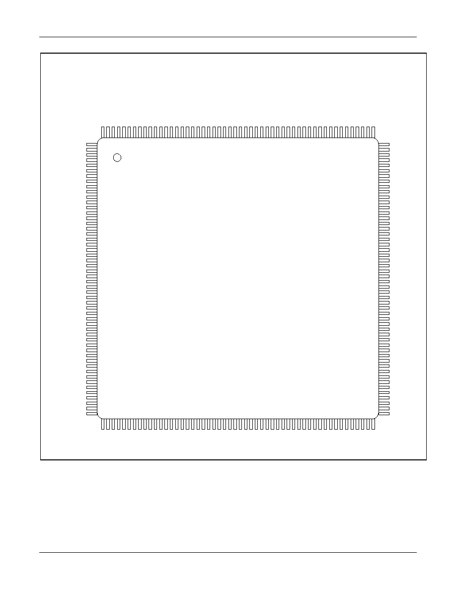
Figure 6. MFC1000 Package Pin Outs - 208-Pin PQFP
�
MD192
15
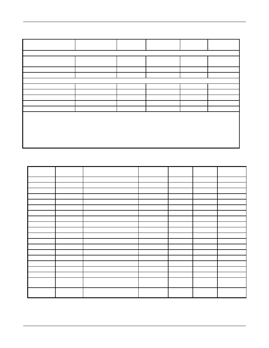
Table 3. Current and Power Requirements
Device
Voltage
(Note 1)
Typical Current
@25∞C (Note 3)
Maximum Current
@ 0∞C (Note 3)
Typical Power
@25∞C (Note 3)
Maximum Power
@ 0∞C (Note 3)
MFC1000
Primary Power
VCC
VDD
+5VDC +5%/-10%
+3VDC +5%/-10%
100 mA
TBD
300 mW
TBD
Battery Power for DRAM
3 VDC
100 mA
TBD
300 mW
TBD
Battery Power for RTC/SRAM
3 VDC
70mA
TBD
60 mW
TBD
MONOFAX Modems
FM209
+5 VDC ±5%
50 mA
55 mA
250 mW
289 mW
FM214
+5 VDC ±5%
54 mA
60 mA
300 mW
315 mW
FM214-V/FM209-V
+5 VDC ±5%
100/2 mA
119/2.5 mA
500/10 mw
625/13.1 mW
FM214-VS/FM209-VS
+5 VDC ±5% (Note 4)
124/2.15 mA
149/2.8 mA
620/2.15 mw
782/14.7 mW
FM336
+5 VDC ±5%
128/1.8 mA
161/2.3 mA
620/9 mW
845/12.3 mW
Notes:
1.
Input voltage ripple =0.1 volts peak-to-peak. The amplitude of any frequency between 20 and 150 kHz must be less than 500
microvolts peak.
2.
Real-Time Clock (RTC) battery power measurements made with a 32.768 kHz crystal oscillator.
3.
Normal/Standby modes.
4.
Modem and XIA combined.
5.
Test conditions: VCC = 5.0 VDC and VDD = 3.0 VDC for typical values; VCC = 5.25 VDC and VDD = 3.0 VDC for maximum values.
Table 4. Operating and Absolute Maximum Ratings
Signal
Input
Type
Description
Operating
(V min)
Operating
(V max)
Abs. Max.
(V min)
Abs. Max.
(V max)
SEN IN
TA
Thermal ADC Head Analog Input
0.2*DADV
0.8*DADV
≠0.5
DADV+0.5
VIN
VA
Video Analog In
-VR
+VR
-0.5
VADV + 0.5
IVREF
+
+IVR
Internal A/D +Vref
3.63
3.74
-
-
IVRE
-
-IVR
Internal A/D -Vref
1.31
2.6
-
-
VREF
+
+VR
Video A/D +Vref
3.0
5.0
-0.5
VADV + 0.5
VRE
-
-VR
Video A/D -Vref
0.0
1.5
-0.5
VADV + 0.5
ADXG
VAXG
+2.5V Analog Reference
2.4
2.6
-
-
ADVA
VADV
Video A/D Power
DADV-0.1
DADV + 0.1
-0.5
7.0
ADGA
VADG
Video A/D GND
-0.1
0.1
-0.5
0.5
ADVD
DADV
Digital A/D Power
4.5
5.25
-0.5
7.0
ADGD
DADG
Digital A/D GND
-0.1
0.1
-0.5
0.5
VDD
VDD
Digital Power
3.0
3.6
≠0.5
6.0
VSS
GND
Digital Ground
0
0
0
0
VGG
VGG
ESD Power
4.75
5.25
-0.5
7.0
VDRAM
VDRAM
Battery Power for DRAM
2.25
3.6
≠0.5
6.0
VBAT
VBAT
Battery Power for RTC/SRAM
2.25
3.6
≠0.5
6.0
DI3V
Digital Input (3V)
-0.5
VDD + 0.5
DI5V
Digital Input (5V)
-0.5
VGG + 0.5
VHz
Voltage applied to outputs in
High-Z State (VDD powered)
-0.5
VDD + 0.5
VGG-VDD
ESD Power to digital power
differential
-0.5
6.0

�
literature@conexant.com
1-800-854-8099 (North America)
33-14-906-3980 (International)
www.conexant.com
World Headquarters
Conexant Systems, Inc.
4311 Jamboree Road
P. O. Box C
Newport Beach, CA
92658-8902
Phone: (949) 483-4600
Fax: (949) 483-6375
�
Phone: (813) 799-8406
Fax: (813) 799-8306
Phone: (805) 376-0559
Fax: (805) 376-8180
Phone: (215) 244-6784
Fax: (215) 244-9292
Phone: (630) 773-3454
Fax: (630) 773-3907
Phone: (978) 692-7660
Fax: (978) 692-8185
!
Phone: (408) 249-9696
Fax: (408) 249-7113
Phone: (972) 773-0723
Fax: (972) 407-0639
Phone: (770) 246-8283
Fax: (770) 246-0018
Phone: (949) 222-9119
Fax: (949) 222-0620
APAC Headquarters
Conexant Systems Singapore,
Pte. Ltd.
1 Kim Seng Promenade
Great World City
#09-01 East Tower
Singapore 237994
Phone: (65) 737 7355
Fax: (65) 737 9077
Phone: (61 2) 9869 4088
Fax: (61 2) 9869 4077
Phone: (86 2) 6361 2515
Fax: (86 2) 6361 2516
" #
Phone: (852) 2827 0181
Fax: (852) 2827 6488
Phone: (91 11) 692 4780
Fax: (91 11) 692 4712
#
Phone: (82 2) 565 2880
Fax: (82 2) 565 1440
Europe Headquarters
Conexant Systems France
Les Taissounieres B1
1680 Route des Dolines
BP 283
06905 Sophia Antipolis Cedex
France
Phone: (33 4) 93 00 33 35
Fax: (33 4) 93 00 33 03
$%
Phone: (49 89) 829 1320
Fax: (49 89) 834 2734
$%
Phone: (39 02) 9317 9911
Fax: (39 02) 9317 9913
$%
Phone: (44 1344) 486 444
Fax: (44 1344) 486 555
$%
Phone: (33 1) 41 44 36 50
Fax: (33 1) 41 44 36 90
Middle East
Headquarters
Conexant Systems Commercial
(Israel) Ltd.
P. O. Box 12660
Herzlia 46733, Israel
Phone: (972 9) 952 4064
Fax: (972 9) 951 3924
Japan Headquarters
Conexant Systems Japan Co.,
Ltd.
Shimomoto Building
1-46-3 Hatsudai,
Shibuya-ku, Tokyo
151-0061 Japan
Phone: (81 3) 5371 1567
Fax: (81 3) 5371-1501
Taiwan Headquarters
Conexant Systems, Taiwan Co.,
Ltd.
Room 2808, 333
International Trade Building
Keelung Road, Section 1
Taipei 110, Taiwan, ROC
Phone: (886 2) 2720 0282
Fax: (886 2) 2757 6760