 | –≠–ª–µ–∫—Ç—Ä–æ–Ω–Ω—ã–π –∫–æ–º–ø–æ–Ω–µ–Ω—Ç: RC224ATLV | –°–∫–∞—á–∞—Ç—å:  PDF PDF  ZIP ZIP |
Data Sheet
D224ATLVDSC
March 25, 1999
RC224ATL/224ATLV
EmbeddedModem Family
The new Conexant RC224ATL utilizes a new integrated data pump/controller to allow
the device to directly connect to host processors that are 3.3 V I/O capable. The codec
used in the new part is the same as the codec used in the existing RC224ATL. The
new device is form, fit, and function compatible with the existing device. This means
there are no hardware and software differences between the existing and the new part,
with one exception. The 3.3 V I/O capable part incorporates 3.3 V compatible digital
I/O buffers, hence requiring 3.3 V digital supply instead of 5 V digital supply.
In addition, unlike the current version of RC224ATL, the new part provides both
data and fax capabilities.
Data modes, controlled by an industry standard 2400 AT command set, can
transmit and receive up to 2400 bps.
Fax modes, controlled by a built-in EIA-578 Class 1 command interface, provide
Group 3 transmit and receive functions.
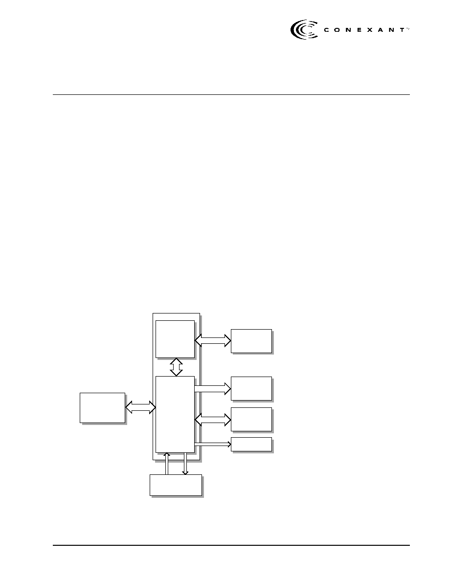
Functional Block Diagram
V.24
EIA-232-D
Interface
Modem
Data Pump
Modem
Controller
Crystal
Telephone
Line
Interface
Modem
LED
Indictors
Optional
NVRAM
Optional
Speaker
Distinguishing Features
∑
Data modes
≠ CCITT V.22 bis (2400 bps), V.22
(1200 bps)
≠ Bell 212A (1200 bps) and 103
(300 bps)
≠ Enhanced AT commands
∑
Group 3 fax modes
≠ V.29 (9600/7200 bps) transmit
≠ V.27 ter (4800/2400 bps)
transmit and receive
≠ V.21 Channel 2 (300 bps)
transmit and receive
∑
EIA-578 Service Class 1 commands
∑
V.42/MNP2-4 and V.42 bis/MNP 5
can be supported through host
software without additional hardware
∑
Data/fax discriminator and auto
answering
∑
Communications software
compatible
∑
Integrated call progress and dialing
∑
No external microcomputer or
memory required
∑
Parallel or serial asynchronous DTE
interface
∑
A/A1 relay control
∑
NVRAM interface allows storage of
two user configurations and four
36-digit dial strings
∑
Automatic adaptive/fixed
compromise equalization
∑
Programmable sleep mode and
wake-up
∑
Full-duplex data mode test
capabilities: Analog loop, local digital
loop, and remote digital loop
∑
Half-duplex fax mode test capabilities
∑
Automatic format/speed sensing
∑
Low power consumption (typical)
≠ Operating: 100 mW
≠ Sleep--Idle: 25 mW
≠ Sleep--Stop: 5 mW
∑
Single +5 V power supply or Dual
+ 3.3 VDD and + 5 VAA power
supplies
∑
Package options:
≠ 68-pin plastic leaded chip carrier
(PLCC)
≠ 100-pin plastic quad flat pack
(PQFP)

D224ATLVDSC
Conexant
Information provided by Conexant Systems, Inc. (Conexant) is believed to be accurate and reliable. However, no responsibility is
assumed by Conexant for its use, nor any infringement of patents or other rights of third parties which may result from its use. No
license is granted by implication or otherwise under any patent rights of Conexant other than for circuitry embodied in Conexant
products. Conexant reserves the right to change circuitry at any time without notice. This document is subject to change without
notice.
Conexant and "What's Next in Communications Technologies" are trademarks of Conexant Systems, Inc.
Product names or services listed in this publication are for identification purposes only, and may be trademarks or registered
trademarks of their respective companies. All other marks mentioned herein are the property of their respective holders.
© 1999 Conexant Systems, Inc.
Printed in U.S.A.
All Rights Reserved
Reader Response: To improve the quality of our publications, we welcome your feedback. Please send comments or
suggestions via e-mail to
Conexant Reader Response@conexant.com
. Sorry, we can't answer your technical
questions at this address. Please contact your local Conexant
sales office
or local field applications engineer if you
have technical questions.
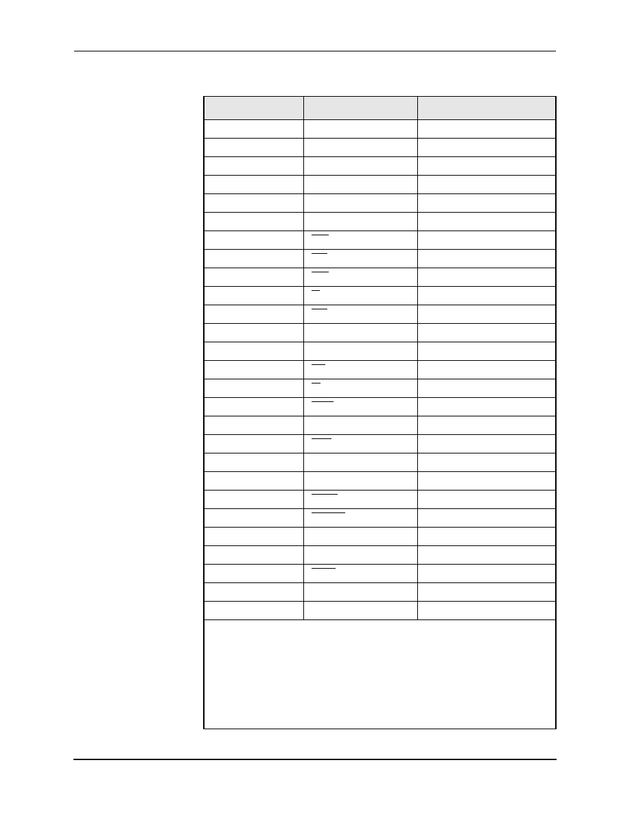
Ordering Information
Replacement Matrix
Marketing
Number
Manufacturing
Number
DSP Die
Number
I/O & VCC
VAA/Codec
Package
RC224ATL
R6781-11
L2501
5V
5V
68 PLCC
RC224ATL
R6781-12
L2501
5V
5V
100 PQFP
RC224ATL
R6781-13
L2503
5V
5V
68 PLCC
RC224ATL
R6781-14
L2503
5V
5V
100 PQFP
RC224ATLV
R6781-21
L2531
3V
5V
68 PLCC
RC224ATLV
R6781-22
L2531
3V
5V
100 PQFP
Marketing
Number
Manufacturing
Number
Package
Replaces
RC224ATL
R6781-11
68 PLCC
RC224ATL/V (R6641-14), RC224ATL (R6641-15),
RC224ATL/VN (R6641-16), RC224ATLN (R6641-17),
RC224ATL/VE (R6641-24), RC224ATLE (R6641-25)
RC224ATL
R6781-12
100 PQFP
RC224ATL/V (R6641-18), RC224ATL (R6641-19),
RC224ATL/VN (R6641-20), RC224ATLN (R6641-21),
RC224ATL/VE (R6641-26), RC224ATLE (R6641-27)
RC224ATL
R6781-13
68 PLCC
RC224ATL/VN (R6641-36), RC224ATL/V
(R6641-37), RC224ATLN (R6641-38), RC224ATL
(R6641-39)
RC224ATL
R6781-14
100 PQFP
RC224ATL/VN (R6641-40), RC224ATATL/V
(R6641-41), RC224ATL (R6641-43)
RC224ATLV
R6781-21
68 PLCC
N/A: New 3.3 V Digital I/O
RC224ATLV
R6781-22
100 PQFP
N/A: New 3.3 V Digital I/O

D224ATLVDSC
Conexant
iii
Table of Contents
List of Figures
. . . . . . . . . . . . . . . . . . . . . . . . . . . . . . . . . . . . . . . . . . . . . . . . . . . . . . . . . . . . . . . . . . . . . . . . vii
List of Tables
. . . . . . . . . . . . . . . . . . . . . . . . . . . . . . . . . . . . . . . . . . . . . . . . . . . . . . . . . . . . . . . . . . . . . . . . . . ix
1.0
Functional Description
. . . . . . . . . . . . . . . . . . . . . . . . . . . . . . . . . . . . . . . . . . . . . . . . . . . . . . . . . . 1-1
1.1
Overview
. . . . . . . . . . . . . . . . . . . . . . . . . . . . . . . . . . . . . . . . . . . . . . . . . . . . . . . . . . . . . . . . . . 1-1
1.2
Technical Specifications
. . . . . . . . . . . . . . . . . . . . . . . . . . . . . . . . . . . . . . . . . . . . . . . . . . . . . . 1-1
1.2.1
General . . . . . . . . . . . . . . . . . . . . . . . . . . . . . . . . . . . . . . . . . . . . . . . . . . . . . . . . . . . . . . . .
1-1
1.2.2
Configurations and Rates . . . . . . . . . . . . . . . . . . . . . . . . . . . . . . . . . . . . . . . . . . . . . . . . . .
1-2
1.2.3
Operation. . . . . . . . . . . . . . . . . . . . . . . . . . . . . . . . . . . . . . . . . . . . . . . . . . . . . . . . . . . . . . .
1-3
1.2.3.1
Data Modes . . . . . . . . . . . . . . . . . . . . . . . . . . . . . . . . . . . . . . . . . . . . . . . . . . . .
1-3
1.2.3.2
Fax Modes . . . . . . . . . . . . . . . . . . . . . . . . . . . . . . . . . . . . . . . . . . . . . . . . . . . . .
1-3
1.2.4
Data/Fax Auto Answering. . . . . . . . . . . . . . . . . . . . . . . . . . . . . . . . . . . . . . . . . . . . . . . . . . .
1-3
1.2.5
Data Modulation . . . . . . . . . . . . . . . . . . . . . . . . . . . . . . . . . . . . . . . . . . . . . . . . . . . . . . . . .
1-3
1.2.6
Equalization . . . . . . . . . . . . . . . . . . . . . . . . . . . . . . . . . . . . . . . . . . . . . . . . . . . . . . . . . . . . .
1-3
1.2.7
Scrambler/Descrambler. . . . . . . . . . . . . . . . . . . . . . . . . . . . . . . . . . . . . . . . . . . . . . . . . . . .
1-3
1.2.8
Transmit Level . . . . . . . . . . . . . . . . . . . . . . . . . . . . . . . . . . . . . . . . . . . . . . . . . . . . . . . . . . .
1-4
1.2.9
Transmit Tones . . . . . . . . . . . . . . . . . . . . . . . . . . . . . . . . . . . . . . . . . . . . . . . . . . . . . . . . . .
1-4
1.2.10
Receive Level. . . . . . . . . . . . . . . . . . . . . . . . . . . . . . . . . . . . . . . . . . . . . . . . . . . . . . . . . . . .
1-4
1.2.11
Receiver Tracking . . . . . . . . . . . . . . . . . . . . . . . . . . . . . . . . . . . . . . . . . . . . . . . . . . . . . . . .
1-4
1.2.12
Low Power Sleep Mode. . . . . . . . . . . . . . . . . . . . . . . . . . . . . . . . . . . . . . . . . . . . . . . . . . . .
1-5
2.0
Hardware Interface
. . . . . . . . . . . . . . . . . . . . . . . . . . . . . . . . . . . . . . . . . . . . . . . . . . . . . . . . . . . . . 2-1
2.1
Hardware Interface
. . . . . . . . . . . . . . . . . . . . . . . . . . . . . . . . . . . . . . . . . . . . . . . . . . . . . . . . . . 2-6
2.1.1
Parallel Interface . . . . . . . . . . . . . . . . . . . . . . . . . . . . . . . . . . . . . . . . . . . . . . . . . . . . . . . . .
2-6
2.1.2
Serial/Indicator Interface . . . . . . . . . . . . . . . . . . . . . . . . . . . . . . . . . . . . . . . . . . . . . . . . . .
2-12
2.1.3
Speaker Interface. . . . . . . . . . . . . . . . . . . . . . . . . . . . . . . . . . . . . . . . . . . . . . . . . . . . . . . .
2-12
2.1.4
Line Interface. . . . . . . . . . . . . . . . . . . . . . . . . . . . . . . . . . . . . . . . . . . . . . . . . . . . . . . . . . .
2-12
2.2
Additional Information
. . . . . . . . . . . . . . . . . . . . . . . . . . . . . . . . . . . . . . . . . . . . . . . . . . . . . . 2-12

Table of Contents
RC224ATL/224ATLV
EmbeddedModem Family
iv
Conexant
D224ATLVDSC
3.0
Pin Descriptions
. . . . . . . . . . . . . . . . . . . . . . . . . . . . . . . . . . . . . . . . . . . . . . . . . . . . . . . . . . . . . . . . 3-1
4.0
AT Commands
. . . . . . . . . . . . . . . . . . . . . . . . . . . . . . . . . . . . . . . . . . . . . . . . . . . . . . . . . . . . . . . . . . 4-1
5.0
S Registers
. . . . . . . . . . . . . . . . . . . . . . . . . . . . . . . . . . . . . . . . . . . . . . . . . . . . . . . . . . . . . . . . . . . . 5-1
6.0
Operation
. . . . . . . . . . . . . . . . . . . . . . . . . . . . . . . . . . . . . . . . . . . . . . . . . . . . . . . . . . . . . . . . . . . . . . 6-1
6.1
Data Modes
. . . . . . . . . . . . . . . . . . . . . . . . . . . . . . . . . . . . . . . . . . . . . . . . . . . . . . . . . . . . . . . . 6-1
6.1.1
Data Mode Selection . . . . . . . . . . . . . . . . . . . . . . . . . . . . . . . . . . . . . . . . . . . . . . . . . . . . . .
6-1
6.1.2
Data Modem Processing . . . . . . . . . . . . . . . . . . . . . . . . . . . . . . . . . . . . . . . . . . . . . . . . . . .
6-1
6.1.3
Call Origination . . . . . . . . . . . . . . . . . . . . . . . . . . . . . . . . . . . . . . . . . . . . . . . . . . . . . . . . . .
6-2
6.1.4
Call Answering. . . . . . . . . . . . . . . . . . . . . . . . . . . . . . . . . . . . . . . . . . . . . . . . . . . . . . . . . . .
6-2
6.1.5
Call Termination. . . . . . . . . . . . . . . . . . . . . . . . . . . . . . . . . . . . . . . . . . . . . . . . . . . . . . . . . .
6-2
6.2
Fax Modes
. . . . . . . . . . . . . . . . . . . . . . . . . . . . . . . . . . . . . . . . . . . . . . . . . . . . . . . . . . . . . . . . 6-3
6.2.1
Fax Mode Selection . . . . . . . . . . . . . . . . . . . . . . . . . . . . . . . . . . . . . . . . . . . . . . . . . . . . . . .
6-3
6.2.2
Fax Mode Processing . . . . . . . . . . . . . . . . . . . . . . . . . . . . . . . . . . . . . . . . . . . . . . . . . . . . .
6-3
6.2.3
Fax Origination . . . . . . . . . . . . . . . . . . . . . . . . . . . . . . . . . . . . . . . . . . . . . . . . . . . . . . . . . .
6-3
6.2.4
Fax Answering . . . . . . . . . . . . . . . . . . . . . . . . . . . . . . . . . . . . . . . . . . . . . . . . . . . . . . . . . . .
6-3
6.2.5
Fax Data Transmission. . . . . . . . . . . . . . . . . . . . . . . . . . . . . . . . . . . . . . . . . . . . . . . . . . . . .
6-4
6.2.6
Fax Data Reception . . . . . . . . . . . . . . . . . . . . . . . . . . . . . . . . . . . . . . . . . . . . . . . . . . . . . . .
6-4
6.2.7
Fax Control Transmission . . . . . . . . . . . . . . . . . . . . . . . . . . . . . . . . . . . . . . . . . . . . . . . . . .
6-4
6.2.8
Fax Control Reception . . . . . . . . . . . . . . . . . . . . . . . . . . . . . . . . . . . . . . . . . . . . . . . . . . . . .
6-5
6.2.9
Fax I/O Processing. . . . . . . . . . . . . . . . . . . . . . . . . . . . . . . . . . . . . . . . . . . . . . . . . . . . . . . .
6-5
6.3
Fax Enhanced Flow Control
. . . . . . . . . . . . . . . . . . . . . . . . . . . . . . . . . . . . . . . . . . . . . . . . . . . . 6-7
6.3.1
Parallel/Serial Interface Selection . . . . . . . . . . . . . . . . . . . . . . . . . . . . . . . . . . . . . . . . . . . .
6-7
6.3.2
Fax V.42 Buffer Sizes . . . . . . . . . . . . . . . . . . . . . . . . . . . . . . . . . . . . . . . . . . . . . . . . . . . . . .
6-7
6.3.3
DTE Flow Control Operation . . . . . . . . . . . . . . . . . . . . . . . . . . . . . . . . . . . . . . . . . . . . . . . .
6-8
6.4
Data/Fax Auto Answering
. . . . . . . . . . . . . . . . . . . . . . . . . . . . . . . . . . . . . . . . . . . . . . . . . . . . . 6-8
6.5
Call Progress
. . . . . . . . . . . . . . . . . . . . . . . . . . . . . . . . . . . . . . . . . . . . . . . . . . . . . . . . . . . . . 6-12
6.5.1
Call Progress Algorithms. . . . . . . . . . . . . . . . . . . . . . . . . . . . . . . . . . . . . . . . . . . . . . . . . .
6-12
6.5.2
Ring Detection. . . . . . . . . . . . . . . . . . . . . . . . . . . . . . . . . . . . . . . . . . . . . . . . . . . . . . . . . .
6-13
7.0
Electrical/Mechanical Specifications
. . . . . . . . . . . . . . . . . . . . . . . . . . . . . . . . . . . . . . . . . . . . . 7-1
7.1
Interfacing the RC224ATLV
. . . . . . . . . . . . . . . . . . . . . . . . . . . . . . . . . . . . . . . . . . . . . . . . . . . . 7-1
7.2
Environmental Requirements
. . . . . . . . . . . . . . . . . . . . . . . . . . . . . . . . . . . . . . . . . . . . . . . . . . 7-1
7.3
Interface Timing and Waveforms
. . . . . . . . . . . . . . . . . . . . . . . . . . . . . . . . . . . . . . . . . . . . . . . . 7-2
Appendix A: RC224ATF Modem Designs
. . . . . . . . . . . . . . . . . . . . . . . . . . . . . . . . . . . . . . . . . . . . . . . . A-1
A.1
68-Pin PLCC Design for Serial Interface
. . . . . . . . . . . . . . . . . . . . . . . . . . . . . . . . . . . . . . . . . . A-1
A.2
68-Pin PLCC Design for Parallel Interface
. . . . . . . . . . . . . . . . . . . . . . . . . . . . . . . . . . . . . . . . . A-6
Appendix B: Acronyms/Abbreviations
. . . . . . . . . . . . . . . . . . . . . . . . . . . . . . . . . . . . . . . . . . . . . . . . . . B-1

RC224ATL/224ATLV
List of Figures
EmbeddedModem Family
D224ATLVDSC
Conexant
v
List of Figures
Figure 2-1.
RC224ATLV Signals--Parallel Interface . . . . . . . . . . . . . . . . . . . . . . . . . . . . . . . . . . . . . . . 2-2
Figure 2-2.
RC224ATLV Signals--Serial Interface. . . . . . . . . . . . . . . . . . . . . . . . . . . . . . . . . . . . . . . . . 2-3
Figure 3-1.
68-Pin PLCC Package--Serial. . . . . . . . . . . . . . . . . . . . . . . . . . . . . . . . . . . . . . . . . . . . . . . 3-1
Figure 3-2.
68-Pin PLCC Package--Parallel . . . . . . . . . . . . . . . . . . . . . . . . . . . . . . . . . . . . . . . . . . . . . 3-2
Figure 3-3.
100-Pin PQFP Package--Serial. . . . . . . . . . . . . . . . . . . . . . . . . . . . . . . . . . . . . . . . . . . . . . 3-3
Figure 3-4.
100-Pin PQFP Package--Parallel . . . . . . . . . . . . . . . . . . . . . . . . . . . . . . . . . . . . . . . . . . . . 3-4
Figure 3-5.
NVRAM Timing . . . . . . . . . . . . . . . . . . . . . . . . . . . . . . . . . . . . . . . . . . . . . . . . . . . . . . . . . 3-20
Figure 7-1.
Timing Waveform . . . . . . . . . . . . . . . . . . . . . . . . . . . . . . . . . . . . . . . . . . . . . . . . . . . . . . . . 7-3
Figure 7-2.
68-Pin PLCC . . . . . . . . . . . . . . . . . . . . . . . . . . . . . . . . . . . . . . . . . . . . . . . . . . . . . . . . . . . . 7-7
Figure 7-3.
100-Pin PQFP . . . . . . . . . . . . . . . . . . . . . . . . . . . . . . . . . . . . . . . . . . . . . . . . . . . . . . . . . . . 7-9
Figure A-1.
Serial Interface Design . . . . . . . . . . . . . . . . . . . . . . . . . . . . . . . . . . . . . . . . . . . . . . . . . . . . A-2
Figure A-2.
Serial Interface Design DAA . . . . . . . . . . . . . . . . . . . . . . . . . . . . . . . . . . . . . . . . . . . . . . . . A-3
Figure A-3.
Parallel Interface Design . . . . . . . . . . . . . . . . . . . . . . . . . . . . . . . . . . . . . . . . . . . . . . . . . . . A-7
Figure A-4.
Parallel Interface Design DAA . . . . . . . . . . . . . . . . . . . . . . . . . . . . . . . . . . . . . . . . . . . . . . . A-8

List of Figures
RC224ATL/224ATLV
EmbeddedModem Family
vi
Conexant
D224ATLVDSC

RC224ATL/224ATLV
List of Tables
EmbeddedModem Family
D224ATLVDSC
Conexant
vii
List of Tables
Table 1-1.
Configurations and Rates . . . . . . . . . . . . . . . . . . . . . . . . . . . . . . . . . . . . . . . . . . . . . . . . . . . 1-2
Table 1-2.
Data Rates vs. Connection Modem Rate . . . . . . . . . . . . . . . . . . . . . . . . . . . . . . . . . . . . . . . . 1- 3
Table 1-3.
Dial Digits/Tone Pairs . . . . . . . . . . . . . . . . . . . . . . . . . . . . . . . . . . . . . . . . . . . . . . . . . . . . . . 1-4
Table 1-4.
Current and Power Requirements . . . . . . . . . . . . . . . . . . . . . . . . . . . . . . . . . . . . . . . . . . . . . 1-5
Table 2-1.
Parallel Interface Registers . . . . . . . . . . . . . . . . . . . . . . . . . . . . . . . . . . . . . . . . . . . . . . . . . . 2-4
Table 2-2.
Programmable Baud Rates . . . . . . . . . . . . . . . . . . . . . . . . . . . . . . . . . . . . . . . . . . . . . . . . . 2-12
Table 3-1.
RC224ATL/224ATLV 68-Pin PLCC Pin Assignments--Serial Mode . . . . . . . . . . . . . . . . . . . 3-5
Table 3-2.
RC224ATLV 68-Pin PLCC Pin Assignments--Parallel Mode. . . . . . . . . . . . . . . . . . . . . . . . . 3-6
Table 3-3.
RC224ATL/224ATLV 100-Pin PQFP Pin Assignments--Serial . . . . . . . . . . . . . . . . . . . . . . . 3-7
Table 3-4.
RC224ATL/224ATLV 100-Pin PQFP Pin Assignments--Parallel . . . . . . . . . . . . . . . . . . . . . 3-11
Table 3-5.
Hardware Interface Signal Definitions . . . . . . . . . . . . . . . . . . . . . . . . . . . . . . . . . . . . . . . . . 3-15
Table 4-1.
Result Codes and Messages . . . . . . . . . . . . . . . . . . . . . . . . . . . . . . . . . . . . . . . . . . . . . . . . . 4-1
Table 4-2.
AT Command Set Summary . . . . . . . . . . . . . . . . . . . . . . . . . . . . . . . . . . . . . . . . . . . . . . . . . 4-2
Table 4-3.
Fax Command Set Summary. . . . . . . . . . . . . . . . . . . . . . . . . . . . . . . . . . . . . . . . . . . . . . . . . 4-7
Table 5-1.
S Register Summary . . . . . . . . . . . . . . . . . . . . . . . . . . . . . . . . . . . . . . . . . . . . . . . . . . . . . . . 5-2
Table 5-2.
S Register Description . . . . . . . . . . . . . . . . . . . . . . . . . . . . . . . . . . . . . . . . . . . . . . . . . . . . . 5-3
Table 6-1.
Data Rate Selection . . . . . . . . . . . . . . . . . . . . . . . . . . . . . . . . . . . . . . . . . . . . . . . . . . . . . . . . 6-1
Table 6-2.
Terminal Called by a 1200 bps Data Modem . . . . . . . . . . . . . . . . . . . . . . . . . . . . . . . . . . . . 6-10
Table 6-3.
Terminal Called by a Fax Machine . . . . . . . . . . . . . . . . . . . . . . . . . . . . . . . . . . . . . . . . . . . . 6-11
Table 6-4.
Tone Characteristics . . . . . . . . . . . . . . . . . . . . . . . . . . . . . . . . . . . . . . . . . . . . . . . . . . . . . . 6-12
Table 6-5.
Fax Class 1 Calling Sequence . . . . . . . . . . . . . . . . . . . . . . . . . . . . . . . . . . . . . . . . . . . . . . . 6-13
Table 6-6.
Fax Class 1 Answering Sequence . . . . . . . . . . . . . . . . . . . . . . . . . . . . . . . . . . . . . . . . . . . . 6-15
Table 7-1.
Environmental Specifications . . . . . . . . . . . . . . . . . . . . . . . . . . . . . . . . . . . . . . . . . . . . . . . . 7-1
Table 7-2.
Timing≠Host Bus Interface . . . . . . . . . . . . . . . . . . . . . . . . . . . . . . . . . . . . . . . . . . . . . . . . . . 7-2
Table 7-3.
Current and Power Requirements . . . . . . . . . . . . . . . . . . . . . . . . . . . . . . . . . . . . . . . . . . . . . 7-4
Table 7-4.
Absolute Maximum Ratings . . . . . . . . . . . . . . . . . . . . . . . . . . . . . . . . . . . . . . . . . . . . . . . . . 7-4
Table 7-5.
Digital Interface Characteristics. . . . . . . . . . . . . . . . . . . . . . . . . . . . . . . . . . . . . . . . . . . . . . . 7-5
Table 7-6.
Analog Interface Characteristics . . . . . . . . . . . . . . . . . . . . . . . . . . . . . . . . . . . . . . . . . . . . . . 7-6
Table 7-7.
68-Pin PLCC Dimensions . . . . . . . . . . . . . . . . . . . . . . . . . . . . . . . . . . . . . . . . . . . . . . . . . . . 7-8
Table 7-8.
100-Pin PQFP Dimensions . . . . . . . . . . . . . . . . . . . . . . . . . . . . . . . . . . . . . . . . . . . . . . . . . 7-10
Table A-1.
Serial Bill of Materials . . . . . . . . . . . . . . . . . . . . . . . . . . . . . . . . . . . . . . . . . . . . . . . . . . . . . . A-4
Table A-2.
Parallel Billing Materials . . . . . . . . . . . . . . . . . . . . . . . . . . . . . . . . . . . . . . . . . . . . . . . . . . . . A-9

List of Tables
RC224ATL/224ATLV
EmbeddedModem Family
viii
Conexant
D224ATLVDSC

D224ATLVDSC
Conexant
1-1
1
1.0 Functional Description
1.1 Overview
The Conexant RC224ATLV is a combination V.22 bis data and Group 3 fax
CMOS modem in a single VLSI package and is identical to the RC224ATLV. The
RC224ATLV integrated data/fax modem is available in either a 68-pin plastic
leaded chip carrier (PLCC) or a 100-pin plastic quad flat pack (PQFP).
Full error correction (V.42 LAPM, MNP2-4) and data compression (V.42 bis,
MNP 5) capabilities can be supported in the RC224ATLV using the host
communication software.
The modem has a selectable parallel or serial interface to the host data
terminal equipment (DTE). When parallel mode is selected, a 16C450-compatible
interface allows direct connection to a notebook, laptop, or PC-compatible bus
without an external universal asynchronous receive/transmit (UART). When
serial mode is selected, a CCITT V.24 logic-compatible interface with transistor to
transistor logic (TTL) levels is supplied along with indicator outputs.
1.2 Technical Specifications
1.2.1 General
The RC224ATLV modem is a full-featured, self-contained data/fax solution. No
external microcontroller for data or fax control functions is required. Dialing, call
progress, and telephone line interface functions are fully supported and controlled
through the AT command set.
Data modes perform complete handshake and data rate negotiations. All tone
and pattern detection required by the applicable CCITT or Bell standard are
supported.
Fax modes support Group 3 fax requirements. Fax data and fax control (V.21
300 bps), performed by the modem, are controlled and monitored through the fax
EIA-578 Class 1 command interface. Full HDLC formatting, flag
insertion/deletion, and CRC generation/checking is provided.
Both transmit and receive fax data is buffered within the modem. Fax data
transfer to and from the DTE is flow controlled by X-on/X-off.

1.0 Functional Description
RC224ATL/224ATLV
1.2 Technical Specifications
EmbeddedModem Family
1-2
Conexant
D224ATLVDSC
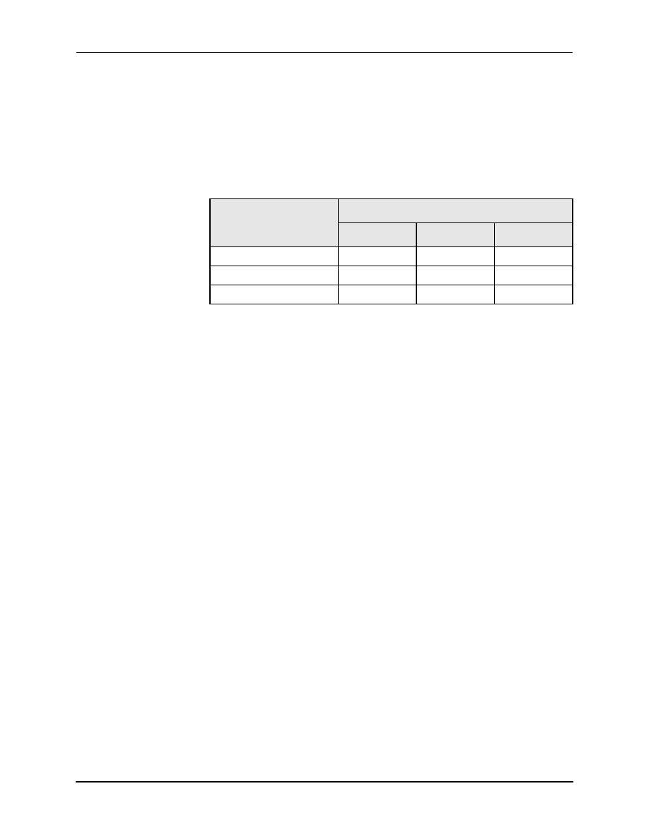
1.2.2 Configurations and Rates
The supported modem configurations and signaling rates are listed in
Table 1-1
.
In data modes with serial interface selected, DTE rate offsets of + 1%, ≠ 2.5% are
accommodated by adding/deleting stop bits as required. In fax modes, the DTE
rate is 19,200 bps.
Table 1-1. Configurations and Rates
Configuration
Modulation
Transmitter Carrier
Frequency (Hz)
±
0.01%
Data Rate
(bps)
Baud
(Symbols/Sec.)
Bits Per
Symbol
Constellation
Points
Data Mode
V.22 bis
V.22
Bell 212A
Bell 103
QAM
DPSK
DPSK
FSK
Answer
2400
2400
2400
2225 M
2025 S
Originate
1200
1200
1200
1270 M
1070 S
2400
1200
1200
300
600
600
600
300
4
2
2
1
16
4
4
1
Fax Mode
V.29
V.27 ter
V.21
QAM
QAM
DPSK
DPSK
FSK
Receive
N/A
N/A
1800
1800
1650 M
1850 S
Transmit
1700
1700
1800
1800
1650 M
1850 S
9600
7200
4800
2400
300
2400
2400
1600
1200
300
4
3
3
2
1
16
8
8
4
1
Legend:
QAM
Quadrature Amplitude Modulation
DPSK
Differential Phase Shift Keying
FSK
Frequency Shift Keying
M
Mark condition
S
Space Condition
N/A
Not Applicable
RC224ATL/224ATLV
1.0 Functional Description
EmbeddedModem Family
1.2 Technical Specifications
D224ATLVDSC
Conexant
1-3
1.2.3 Operation
Modem operation is controlled by AT commands, fax service class 1 commands,
and supporting S registers.
1.2.3.1 Data Modes
Data rate selection is determined by the speed of the originating and answering
modems, as defined in
Table 1-2
.
1.2.3.2 Fax Modes
Fax modes are negotiated as defined in T.30 and are implemented by AT+F
commands. The AT+FCLASS=1 command causes entry into the fax mode from
the data mode. Most other fax class 1 commands, which start with the AT+F
prefix, are valid only in the fax mode. All data commands are valid in the fax
mode except A/, On, &Tn, and the escape sequence (+++). The AT+FCLASS=0
command terminates the fax mode and causes entry into the data mode.
1.2.4 Data/Fax Auto Answering
The modem can automatically determine if the incoming call is from a data or fax
modem, make the appropriate connection, and inform the DTE of the connection
type.
1.2.5 Data Modulation
The data modulation conforms to V.29, V.27 ter, V.22 bis, V.22, V.21, Bell 212A,
or Bell 103, depending on the selected configuration. Transmitter and receiver
spectrum shaping is provided in accordance with the applicable standard.
1.2.6 Equalization
Automatic adaptive equalization and fixed compromised equalization are
provided to compensate for line distortions and to minimize the effects of
intersymbol interference.
1.2.7 Scrambler/Descrambler
The modem incorporates a self-synchronizing scrambler/descrambler, which
satisfies the applicable CCITT or Bell requirements.
Table 1-2. Data Rates vs. Connection Modem Rate
Originate Modem Rate
(bps)
Connect Speed Based on Answer Modem Rate (bps)
300
1200
2400
300
300
300
300
1200
300
1200
1200
2400
300
1200
2400
1.0 Functional Description
RC224ATL/224ATLV
1.2 Technical Specifications
EmbeddedModem Family
1-4
Conexant
D224ATLVDSC
1.2.8 Transmit Level
The transmit level is ≠ 10 dBm
±
1 dB (at TIP and RING) and can be obtained
using the circuits shown in Appendix A. Carrier and dual tone multi-frequency
(DTMF) transmit levels can be further attenuated using AT%Ln + AT%Dn
commands, respectively. If a higher transmit level is required, an external op amp
can be added.
1.2.9 Transmit Tones
Answer Tone
An answer tone of 2100 Hz (V.22 bis, V.22, or T.30) or 2225 Hz (Bell 212A or
103) is generated.
Guard Tone
An 1800 Hz guard tone can be generated in all data modes.
Calling Tone
An 1100 Hz (0.5 seconds on, 3 seconds off) calling tone (T.30) is generated in the
originate fax mode.
1.2.10 Receive Level
The receiver satisfies performance requirements for a received signal from
≠ 9 dBm to ≠ 43 dBm. The carrier detect is ON at ≠ 43 dBm and OFF at ≠ 48 dBm
with a minimum of 2 dB hysteresis.
1.2.11 Receiver Tracking
The modem can accommodate carrier frequency offset up to
±
7 Hz, and a
transmit timing error of
±
0.01% (V.22 bis or V.27 ter) or
±
0.02% (V.22 or Bell
212A).
DTMF Dialing
Standard DTMF tones (digits 0-9, A, B, C, D, *, and #) or pulses (digits 0-9) can
be generated. Refer to
Table 1-3
.
Ring Detection
RING signal is detected from valid high to low transitions on the RING input line
at frequencies of 15.3 Hz to 63 Hz. A RING is valid if the RING ON time is
greater than 0.125 seconds and is followed by a RING OFF time greater than 0.5
seconds.
Table 1-3. Dial Digits/Tone Pairs (1 of 2)
Dial Digit
Tone 1
Frequency (Hz)
Tone 2
Frequency (Hz)
0
941
1336
1
697
1209
2
697
1336
3
697
1477
4
770
1209
5
770
1336
RC224ATL/224ATLV
1.0 Functional Description
EmbeddedModem Family
1.2 Technical Specifications
D224ATLVDSC
Conexant
1-5
1.2.12 Low Power Sleep Mode
To conserve power, the RC224ATLV has two selectable sleep (power-down)
modes ≠ Idle and Stop. If enabled by the IDLEN0 and IDLN1 inputs, the selective
sleep mode is entered whenever the modem is active. The sleep mode indicator
output, SLEEP, is provided to allow external circuits to be powered down when
the modem is in Idle or Stop mode.
The Idle mode allows reduced power consumption with automatic recovery
without additional circuitry. If Idle mode is selected, the modem exits Idle mode
and returns to full operation whenever a ring signal occurs, the DTE writes to the
modem (parallel interface), or WAKEUP input, normally tied to DTR or TXD, is
asserted (serial interface).
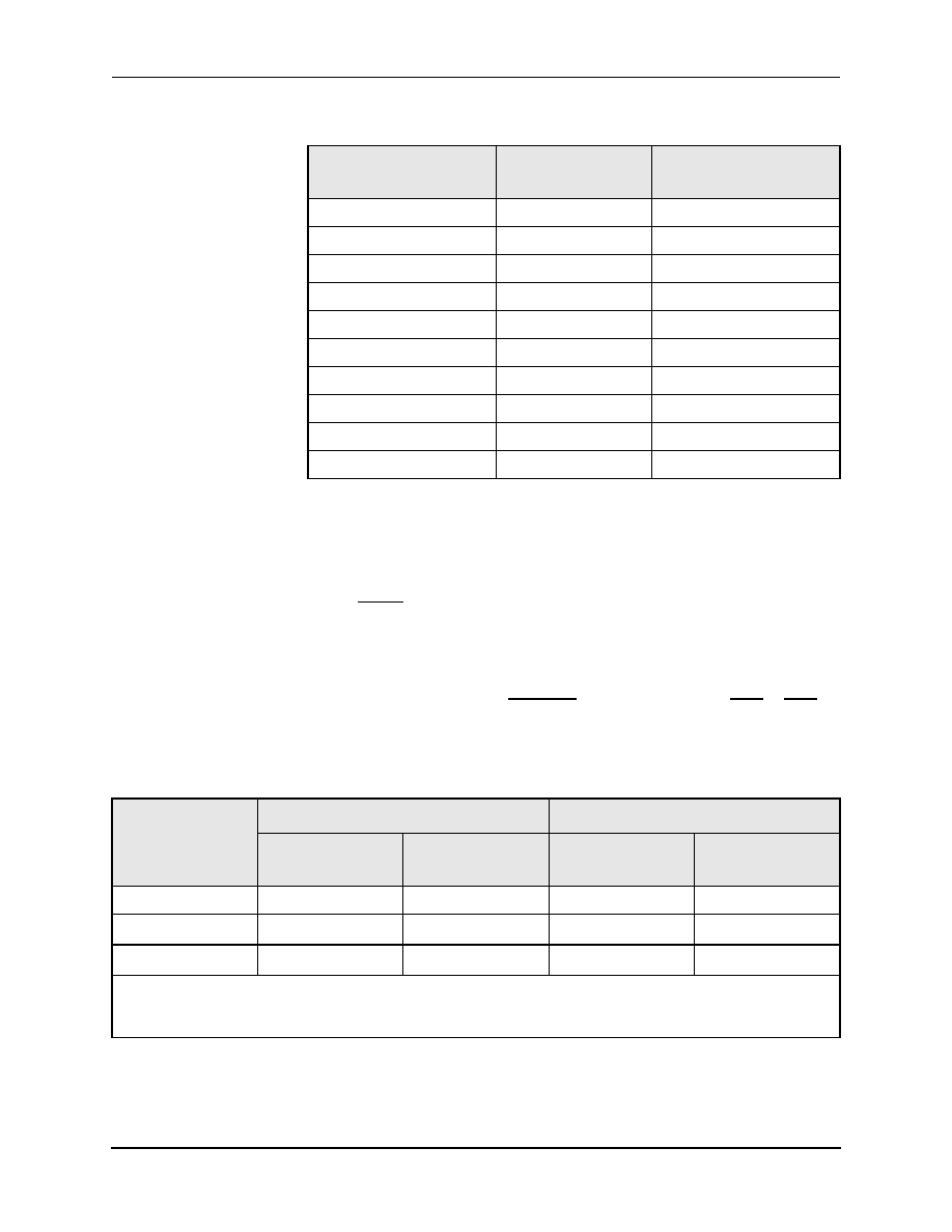
The Stop mode further reduces power consumption, as defined in
Table 1-4
.
6
770
1477
7
852
1209
8
852
1336
9
852
1477
*
941
1209
#
941
1477
A
697
1633
B
770
1633
C
852
1633
D
941
1633
Table 1-3. Dial Digits/Tone Pairs (2 of 2)
Dial Digit
Tone 1
Frequency (Hz)
Tone 2
Frequency (Hz)
Table 1-4. Current and Power Requirements
Mode
Current (ID)
Power (PD)
Typical
Current @ 25
∞
C
Maximum Current
@ 0
∞
C
Typical
Power @ 25
∞
C
Maximum
Power @ 0
∞
C
Operating
21 mA
22 mA
100 mW
110 mW
Sleep
≠
Idle
5 mA
6 mA
25 mW
30 mW
Sleep
≠
Stop
1 mA
1 mA
5 mW
5 mW
NOTE(S):
1. Test conditions: VDD = 5.0 V
DC
for typical values; VDD = 5.25 V
DC
for maximum values.
2. Test conditions: VDD = 3.3 V
DC
for typical values; VDD = 3.6 V
DC
for maximum values.

1.0 Functional Description
RC224ATL/224ATLV
1.2 Technical Specifications
EmbeddedModem Family
1-6
Conexant
D224ATLVDSC
Entry
The modem will enter the low-power sleep mode when no line connection exists
and no host activity occurs for the period of time specified in the S24 register. All
EmbeddedModem circuits are turned off except the internal Microcontroller Unit
(MCU) clock circuitry in order to consume lower power but are able to
immediately wake up and resume normal operation.
Wake-up--Parallel
Interface Configuration
Wake-up occurs when a ring signal occurs, or the host write to the modem.
Wake-up--Serial
Interface Configuration
Wake-up occurs when a ring signal occurs, or the DTE sends a character to the
modem.

D224ATLVDSC
Conexant
2-1
2
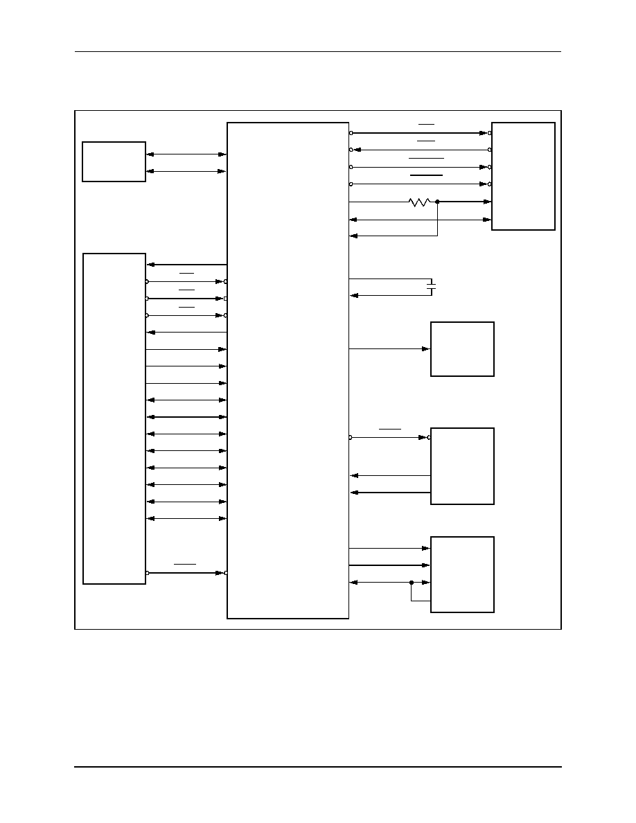
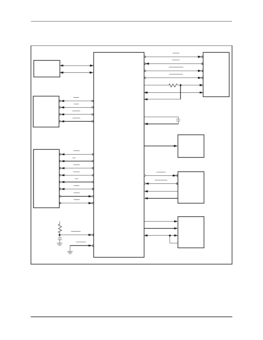
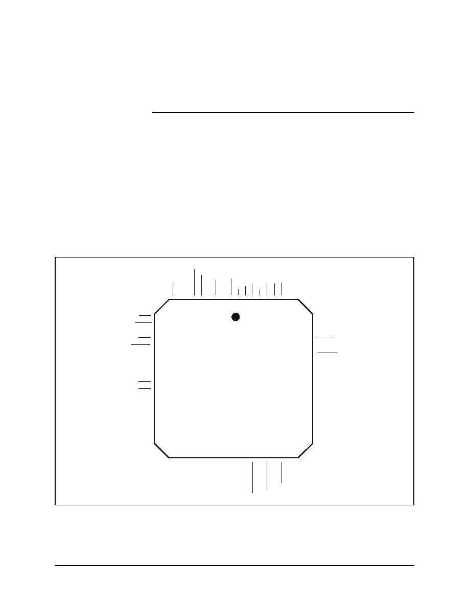
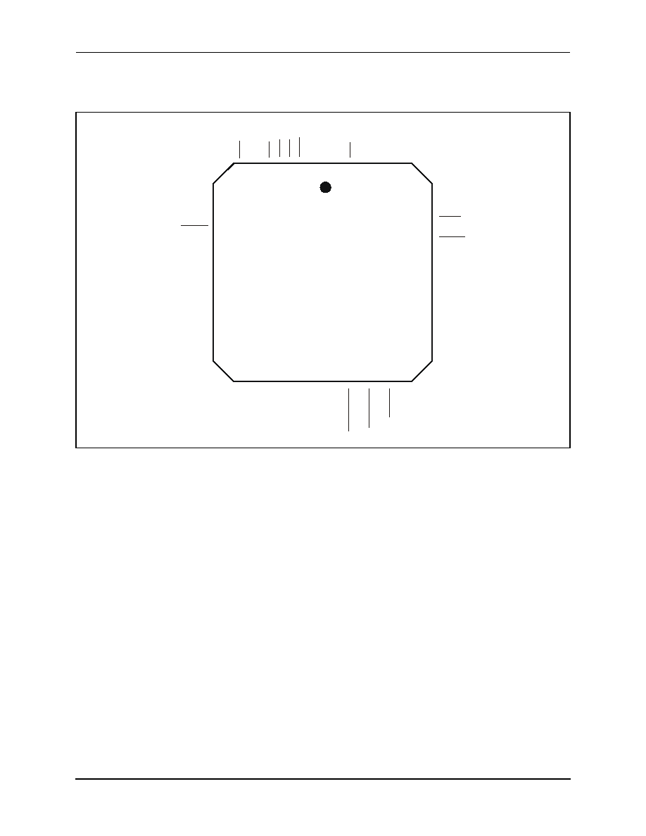
2.0 Hardware Interface
Figure 2-1
and
Figure 2-2
illustrate the RC224ATLV hardware interface signals
for the parallel and serial interfaces, respectively.
The RC224ATLV hardware interface signals are described in
Table 3-5, Hardware Interface Signal Definitions
.
See
Table 7-2, Timing≠Host Bus Interface
for a list of the host bus interface
timing parameters and
Figure 7-1, Timing Waveform
for an illustration of the
interface waveforms.
2.0 Hardware Interface
RC224ATL/224ATLV
EmbeddedModem Family
2-2
Conexant
D224ATLVDSC
Figure 2-1. RC224ATLV Signals--Parallel Interface
Host
Computer
Parallel BUS
Crystal
HDIS
HCS
HRD
HWT
HINT
HA0
HA1
HA2
HD0
HD1
HD2
HD3
HD4
HD5
HD6
HD7
RESET
XTLI
XTLO
RC224ATL
RC224ATLV
MODEM
Optional
NVRCS
NVRSK
NVRAM
NVRDIO
RFILO
AGCIN
Sleep Mode
Interface
SLEEP
IDLEN0
IDLEN1
Optional
Speaker
Amplifier
SPKR
Telephone
Line
Interface
A/A1
RING
TLKRELAY
OHRELAY
TXAI
TXA2
RXA
RC224ATL/224ATLV
2.0 Hardware Interface
EmbeddedModem Family
D224ATLVDSC
Conexant
2-3
Figure 2-2. RC224ATLV Signals--Serial Interface
V.24
EIA-232-D
Interface
Crystal
MR
DCDL
DTRL
RXD
CI/HS
DCD
DSR
RI
CTS
TXD
DTR
RESET
XTLI
XTLO
RC224ATL
RC224ATLV
MODEM
Optional
NVRCS
NVRSK
NVRAM
NVRDIO
RFILO
AGCIN
Sleep Mode
Interface
SLEEP
IDLEN0
IDLEN1
Optional
Speaker
Amplifier
SPKR
Telephone
Line
Interface
A/A1
RING
TLKRELAY
OHRELAY
TXAI
TXA2
RXA
LED
Indicators
WAKEUP
AAE
SEREN
+5 V

2.0 Hardware Interface
RC224ATL/224ATLV
EmbeddedModem Family
2-4
Conexant
D224ATLVDSC
The parallel interface registers are identified in
Table 2-1
.
Table 2-1. Parallel Interface Registers (1 of 2)
Register
Number
Register
Name
Bit Number
7
6
5
4
3
2
1
0
7
Scratch
Register
(SCR)
Scratch Register
6
Modem
Status
Register
(MSR)
Data
Carrier
Detect
(DCD)
Ring
Indicator
(RI)
Data Set
Ready
(DSR)
Clear to
Send (CTS)
Delta Data
Carrier
Detect
(DDCD)
Trailing
Edge of
Ring
Indicator
(TERI)
Delta Data
Set Ready
(DDSR)
Delta Clear
to Send
(DCTS)
5
Line Status
Register
(LSR)
0
Transmitter
Empty
(TEMT)
Transmitter
Holding
Register
(THRE)
Break
Interrupt
(BI)
Framing
Error (FE)
Parity Error
(PE)
Overrun
Error (OE)
Data Ready
(DR)
4
Modem
Control
Register
(MCR)
0
0
0
Local
Loopback
Out 2
Out 1
Request to
Send (RTS)
Data
Terminal
Ready
(DTR)
3
Line
Control
Register
(LCR)
Divisor
Latch
Access Bit
(DLAB)
Set Break
(SB)
Stick Parity
(SP)
Even Parity
Select
(EPS)
Parity
Enable
(PEN)
Number of
Stop Bits
(STB)
Word
Length
Select Bit 1
(WLS1)
Word
Length
Select Bit 0
(WLS0)
2
Interrupt
Identify
Register
(IIR) (Read
Only)
0
0
0
0
0
Pending
Interrupt ID
Bit 1
(PL1)
Pending
Interrupt ID
Bit 0
(PL0)
0 if
Interrupt
Pending
(IP)
1
DLAB = 0
Interrupt
Enable
Register
(IER)
0
0
0
0
Enable
Modem
Status
Interrupt
(EDSSI)
Enable
Receiver
Line Status
Interrupt
(ELSI)
Enable
Transmitter
Holding
Register
Empty
Interrupt
(ETBEI)
Enable
Received
Data
Available
Interrupt
(ERBFI)
0
DLAB = 0
Transmitter
Holding
Register
(THR)
Transmitter Holding Register (Write Only)
0
DLAB = 0
Receiver
Buffer
Register
(RBR)
Receiver Buffer Register (Read Only)

RC224ATL/224ATLV
2.0 Hardware Interface
EmbeddedModem Family
D224ATLVDSC
Conexant
2-5
1
DLAB = 1
Divisor
Latch MSB
Register
(DLM)
Divisor Latch (MS)
0
DLAB = 1
Divisor
Latch LSB
Register
(DLL)
Divisor Latch (LS)
Table 2-1. Parallel Interface Registers (2 of 2)
Register
Number
Register
Name
Bit Number
7
6
5
4
3
2
1
0

2.0 Hardware Interface
RC224ATL/224ATLV
2.1 Hardware Interface
EmbeddedModem Family
2-6
Conexant
D224ATLVDSC
2.1 Hardware Interface
2.1.1 Parallel Interface
A 16450 UART-compatible parallel interface is provided.
Host Bus Interface
Eight data lines, three address lines, and four control lines are supported.
Interrupt Enable Register
(Addr=1, DLAB=0)
The Interrupt Enable Register (IER) enables four types of interrupts that can
separately assert the HINT output. A selected interrupt can be enabled by setting
the corresponding enable bit to a logic 1, or disabled by resetting the
corresponding enable bit to a logic 0. All interrupt sources are disabled by setting
bits 0≠3 to a logic 0. Disabling all interrupts inhibits the Interrupt Identifier
Register (IIR) and inhibits assertion of the HINT output. All other system
functions operate normally, including the setting of the Line Status Register
(LSR) and the Modem Status Register (MSR).
Bits 4-7:
Not used (always logic 0).
EDSSI
Enable Modem Status Interrupt.
When this bit is a logic 1,
it enables assertion of the HINT output whenever bit 0, 1, 2, or
3 in the Modem Status Register (MSR) is a logic 1. When this
bit is a logic 0, it disables assertion of HINT due to setting of
any of these four MSR bits.
ELSI
Enable Receiver Line Status Interrupt.
When this bit is a
logic 1, it enables assertion of the HINT output when any
receiver status bit in the Line Status Register (LSR); i.e., bits
1, 2, 3, or 4, changes state. When this bit is a logic 0, it
disables assertion of HINT due to change of the receiver LSR
bits.
ETBEI
Enable Transmitter Holding Register Empty Interrupt.
When this bit is a logic 1, it enables assertion of the HINT
output when the Transmitter Holding Register Empty (THRE)
bit in the Line Status Register (LSR5) is set to a logic 1. When
this bit is a logic 0, it disables assertion of HINT due to LSR5.
ERBFI
Enable Received Data Available Interrupt.
When this bit is
a logic 1, it enables assertion of the HINT output when
received data is available in the Receiver Buffer; i. e., the Data
Ready bit in the Line Status Register (LSR0) is a logic 1.
When this bit is a logic 0, it disables assertion of HINT due to
the LSR0.
7
6
5
4
3
2
1
0
0
0
0
0
EDSSI
ELSI
ETBEI
ERBFI
RC224ATL/224ATLV
2.0 Hardware Interface
EmbeddedModem Family
2.1 Hardware Interface
D224ATLVDSC
Conexant
2-7
Interrupt Identifier
Register (Addr = 2)
The Interrupt Identifier Register (IIR) identifies the existence and type of
prioritized pending interrupts. Four priority levels are set to assist interrupt
processing in the host.
When addressed during chip-select time, the IIR freezes the highest priority
interrupt pending and acknowledges no other interrupts until the particular
interrupt is serviced by the host.
Bits 3-7:
Not used (always 0).
PL0-1
Highest Priority Pending Interrupt.
These two bits identify
the highest priority pending interrupt.
Priority
2
1
Level
Pending Interrupt
1
1
(highest)
Receiver Line Status
1
0
2
Receiver Buffer Full
0
1
3
Transmitter Holding Register
Empty
0
0
4
Modem Status
IP
Interrupt Pending
. When this bit is a logic 0, an interrupt is
pending. When this bit is a logic 1, no interrupt is pending.
This bit can be used in a hardwired prioritized or polled
environment to indicate whether an interrupt is pending. If an
interrupt is pending, the IIR contents can be used as a pointer
to the appropriate interrupt service routine in the host.
7
6
5
4
3
2
1
0
0
0
0
0
0
PL1
PL0
IP

2.0 Hardware Interface
RC224ATL/224ATLV
2.1 Hardware Interface
EmbeddedModem Family
2-8
Conexant
D224ATLVDSC
Line Control Register
(Addr = 3)
The Line Control Register (LCR) specifies the format of the asynchronous data
communications exchange.
DLAB
Divisor Latch Access Bit
. This bit must be set to a logic 1 to
access the Divisor latches of the baud generator during a read
or write operation. It must be reset to a logic 0 to access the
Receiver Buffer, the Transmitter Holding Register, or the
Interrupt Enable Register.
SB
Set Break
. When this bit is set to a logic 1, the transmit data is
forced to the space (logic 0) state. The break is disabled by
setting this bit to a logic 0. The Set Break bit acts only on the
transmit data and has no effect on the serial in logic.
SP
Stick Parity
. When stick parity is selected (LCR5 = 1), parity
is enabled (LCR3 = 1), and even parity is selected (LCR4 = 1),
the parity bit is transmitted and checked by the receiver as a
logic 0. When stick parity is selected (LCR5 = 1), parity is
enabled (LCR3 = 1), and odd parity is selected (LCR4 = 0),
the parity bit is transmitted and checked by the receiver as a
logic 1.
EPS
Even Parity Select
. When parity is enabled (LCR3 = 1), and
Stick Parity (LCR5) is a logic 0, the number of logic 1s
transmitted or checked in the data word bits and parity bit is
either even (LCR4 = 1) or odd (LCR4 = 0).
PEN
Parity Enable
. When bit 3 is a logic 1, a parity bit is
generated in the serial out (transmit) data stream and checked
in the serial in (receive) data stream. The parity bit is located
between the last data bit and the first stop bit.
STB
Number of Stop Bits
. This bit specifies the number of stop
bits in each serial out character. If bit 2 is a logic 0, one stop
bit is generated regardless of word length. If bit 2 is a logic 1
when either a 5-, 6-, 7-, or 8-bit word length is selected, two
stop bits are generated. The serial in logic checks the first stop
bit only regardless of the number of stop bits selected.
WLS0 and WLS1 Word Length Select
. These two bits specify the number of
bits in each serial in or serial out character. The encoding of
bits 0 and 1 is:
Bit 1
Bit 0
Word Length
0
0
5 Bits
0
1
6 Bits
1
0
7 Bits
1
1
8 Bits
7
6
5
4
3
2
1
0
DLAB
SB
SP
EPS
PEN
STB
WLS1
WLS0

RC224ATL/224ATLV
2.0 Hardware Interface
EmbeddedModem Family
2.1 Hardware Interface
D224ATLVDSC
Conexant
2-9
Modem Control Register
(Addr = 4)
The Modem Control Register (MCR) controls the interface with the modem or
data set.
Bit 5-7:
Not used (always 0).
LL
Local Loopback
. When this bit is set to a logic 1, the
diagnostic mode is selected and the following occurs:
1.
Data written to the Transmit Holding Register will be
looped back to the Receiver Buffer Register.
2.
The four modem control bits (CTS, DSR, RI, and DCD)
are internally connected to the four modem control
outputs (RTS, DTR, OUT1, and OUT2), respectively.
OUT2
Output 2
. When this bit is a logic 1, HINT is enabled. When
this bit is a logic 0, HINT is in the high impedance state.
OUT1
Output 1
. This bit is used in local loopback (see MCR4).
RTS
Request to Send
. This bit controls the Request to Send (RTS)
function. When this bit is a logic 1, RTS is on. When this bit is
a logic 0, RTS is off.
DTR
Data Terminal Ready
. This bit controls the Data Terminal
Ready (DTR) function. When this bit is a logic 1, DTR is on.
When this bit is a logic 0, DTR is off.
7
6
5
4
3
2
1
0
0
0
0
LL
OUT2
OUT1
RTS
DTR

2.0 Hardware Interface
RC224ATL/224ATLV
2.1 Hardware Interface
EmbeddedModem Family
2-10
Conexant
D224ATLVDSC
Line Status Register
(Addr = 5)
The LSR, an 8-bit register, provides status information to the host concerning data
transfer.
Bit 7:
This bit is set to logic 0.
TEMT
Transmitter Empty
. This bit is set to a logic 1 whenever the
Transmitter Holding Register (THR) and the Transmitter Shift
Register (TSR) are both empty. It is reset to a logic 0 whenever
either the THR or TSR contains a data character.
THRE
Transmitter Holding Register Empty
. This bit indicates that
the modem is ready to accept a new character for
transmission. In addition, this bit causes the modem to issue
an interrupt to the host when the Transmit Holding Register
Empty Interrupt Enable bit (IIR1) is set to logic 1. The THRE
bit is set to a logic 1 when a character is transferred from the
Transmitter Holding Register into the Transmitter Shift
Register. The bit is reset to logic 0 concurrently with the
loading of the Transmitter Holding Register by the host.
BI Break
Interrupt
. This bit is set to a logic 1 whenever the
received data input is a space (logic 0) for longer than two full
word lengths plus 3 bits. The 81 indicator is reset whenever
the host reads the LSR.
FE Framing
Error
. This bit indicates that the received character
did not have a valid stop bit. Bit 3 is set to a logic 1 whenever
the stop bit following the last data bit or parity bit is detected
as a zero bit. The FE bit is reset to a logic 0 whenever the host
reads the LSR.
PE
Parity Error
. This bit indicates that the received data
character does not have the correct even or odd parity, as
selected by the Even Panty Select bit (LCR4) and the Stick
Parity bit (LCR5). The PE bit is set to a logic 1 upon detection
of parity error and is reset to a logic 0 whenever the host reads
the LSR.
OE Overrun
Error
. This bit indicates that data in the Receiver
Buffer Register was not read by the host before the next
character was transferred into the Receiver Buffer Register,
thereby destroying the previous character. The OE bit is reset
whenever the host reads the LSR.
DR
Data Ready
. This bit is set to a logic 1 whenever a complete
incoming character has been received and transferred into the
Receiver Buffer Register. Bit 0 is reset to a logic 0 when the
host reads the Receiver Buffer Register.
7
6
5
4
3
2
1
0
0
TEMT
THRE
BI
FE
PE
OE
DR
RC224ATL/224ATLV
2.0 Hardware Interface
EmbeddedModem Family
2.1 Hardware Interface
D224ATLVDSC
Conexant
2-11
Modem Status Register
(Addr = 6)
The Modem Status Register (MSR) reports the modem's current state and change
information. Bits 4-7 supply current state, and bits 0-3 supply change
information. The change bits are set to a logic 1 whenever a control input from the
modem changes state from the last MSR read by the host. Bits 0-3 are reset to
logic 0 when the host reads the MSR or upon reset.
Whenever Bits 0,1, 2, or 3 are set to a logic 1, a Modem Status Interrupt is
generated.
DCD
Data Carrier Detect
. This bit indicates the logic state of the
DCD output. If Loopback is selected (MCR4 = 1), this bit
reflects the state of OUT2 in the MCR (MCR3).
RI
Ring Indicator
. This bit indicates the logic state of the RI
output. If Loopback is selected (MCR4 = 1), this bit reflects
the state of OUT1 in the MCR (MCR2).
DSR
Data Set Ready
. This bit indicates the logic state of the DSR
output. If Loopback is selected (MCR4 = 1), this bit reflects
the state of DTR in the MCR (MCR0).
CTS
Clear to Send
. This bit indicates the logic state of the CTS
output. If Loopback is selected (MCR4 = 1), this bit reflects
the state of RTS in the MCR (MCR1).
DDCD
Delta Data Carrier Detect
. This bit is set to a logic 1 when
the DCD bit has changed since the MSR was last read by the
host.
TERI
Trailing Edge of Ring Indicator
. This bit is set to a logic 1
when the RI bit changes from a 1 to a 0 state since the MSR
was last read by the host.
DDSR
Delta Data Set Ready
. This bit is set to a logic I when the
DSR bit has changed state since the MSR was last read by the
host.
DCTS
Delta Clear to Send
. This bit is set to a logic 1 when the CTS
bit has changed state since the MSR was last read by the host.
Receiver Buffer Register
(Addr=0, DLAB=0)
The Receiver Buffer Register (RBR) is a read-only register at location 0 (with
DLAB = 0). Bit 0 is the least significant bit of the data, and is the first bit
received.
Transmitter Holding
Register (Addr=0,
DLAB=0)
The Transmitter Holding Register (THR) is a write-only register at address 0
when DLAB = 0. Bit 0 is the least significant bit and the first bit sent.
7
6
5
4
3
2
1
0
DCD
RI
DSR
CTS
DDCD
TERI
DDSR
DCTS

2.0 Hardware Interface
RC224ATL/224ATLV
2.2 Additional Information
EmbeddedModem Family
2-12
Conexant
D224ATLVDSC
Divisor Registers
(Addr=0 and 1, DLAB=1)
The Divisor Latch LS Byte and Divisor Latch MS Byte are two read-write
registers at locations 0 and 1 when DLAB = 1, respectively.
The baud rate is selected by loading each divisor latch with the appropriate
hex value.
Table 2-2
lists the programmable values corresponding to the desired
baud rate.
Scratch Register (SCR)
(Addr = 7)
The Scratchpad Register is a read-write register at location 7. This register is not
used by the DSP and can be used by the host for temporary storage.
2.1.2 Serial/Indicator Interface
A DTE serial interface and indicator outputs are supported.
∑
Serial Interface: An 8-line V.24/EIA-232-D or TTL logic serial interface to
the DTE is supported.
∑
LED Indicator Interface: Four direct connect LED indicator outputs are
supported.
2.1.3 Speaker Interface
A speaker output, controlled by AT or V.25 bis commands, is provided for an
optional OEM-supplied speaker circuit.
2.1.4 Line Interface
The EmbeddedModem connects to the line interface circuitry by means of a
receive analog input, two transmit analog outputs, and a ring signal input.
The EmbeddedModem provides three relay control outputs to the line
interface. These outputs may be used to control relays such as off-hook, A/A1,
and talk/data.
2.2 Additional Information
Additional information is provided in the RC224ATLV Modem Designer's Guide
(Order No. 821).
Table 2-2. Programmable Baud Rates
Divisor Latch (Hex)
Divisor
(Decimal)
Baud Rate
MS
LS
01
00
00
00
80
C0
60
30
384
192
96
48
300
600
1200
2400
D224ATLVDSC
Conexant
3-1
3
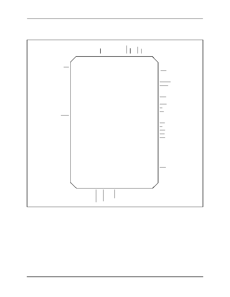
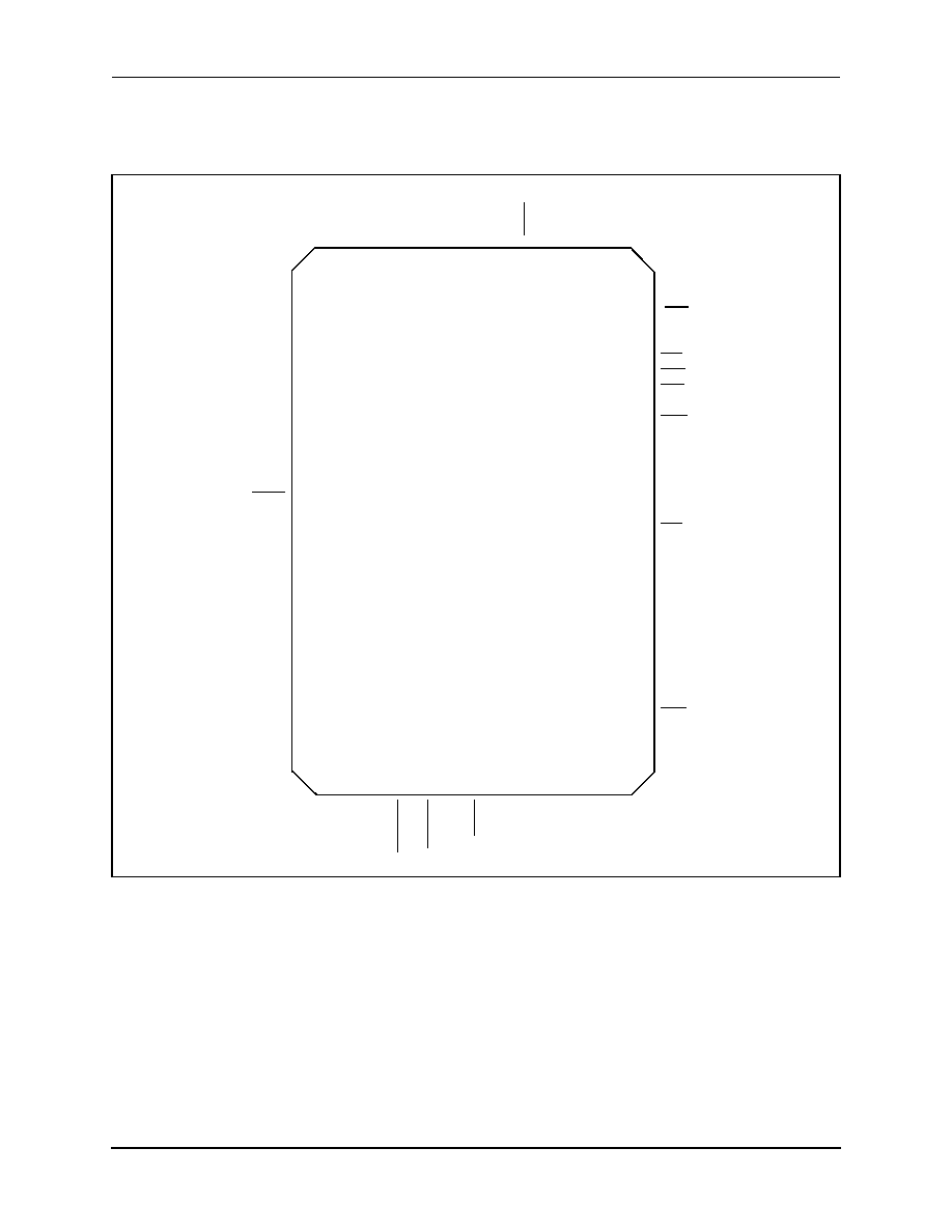
3.0 Pin Descriptions
The RC224ATLV 68-pin PLCC serial and parallel pinouts are displayed in
Figure 3-1
and
Figure 3-2
, respectively. The 100-pin PQFP serial and parallel
pinout diagrams are displayed in
Figure 3-3
and
Figure 3-4
, respectively.
Figure 3-5
displays NVRAM timing.
RC224ATLV 68-pin PLCC serial and parallel pin assignments are displayed in
Table 3-1
and
Table 3-2
, respectively. The 100-pin serial and parallel pin
assignments are displayed in
Table 3-3
and
Table 3-4
, respectively.
Figure 3-1. 68-Pin PLCC Package
--
Serial
AAE
DTRL
NC
RXD
RESET
VCC
NVRSK
NC
NC
TXD
DTR
IDLEN1
RAGCO
RADCI
TSTBO
RSTBO
RRSTO
10
11
12
13
14
15
16
17
18
19
20
21
22
23
24
25
26
DGND1
XTLO
XTLI
TEST
2
SLEEP
SPKR
VAA
MODEI
TSTBI
TRSTI
TDACI
RADCO
RRSTI
NC
RSTBI
NC
60
59
58
57
56
55
54
53
52
51
50
49
48
47
46
45
44
A/
A1
NV
RDI
O
NV
RCS
WA
KE
U
P
SE
REN
NC
RING
IDLEN0
DCDL
RI
MR
NM
I
CI/
H
S
DCD
CTS
DS
R
DGND2
9
8
7
6
5
4
3
2
1
68
67
66
65
64
63
62
61
27
28
29
30
31
32
33
34
35
36
37
38
39
40
41
42
43
T
R
S
TO
MO
DE
O
TD
A
C
O
NC
TX
A2
T
X
A1
RXA
RFI
L
O
AGCIN
VC
NC
T
L
KRE
L
AY
AG
ND
OH
R
E
L
A
Y
NC
S
L
EE
PI
RAGCI
3.0 Pin Descriptions
RC224ATL/224ATLV
EmbeddedModem Family
3-2
Conexant
D224ATLVDSC
Figure 3-2. 68-Pin PLCC Package
--
Parallel
HA1
HA0
IDLEN0
NVRSK
RESET
VCC
HINT
HDIS
NC
NVRDIO
NC
IDLEN1
RAGCO
RADCI
TSTBO
RSTBO
RRSTO
10
11
12
13
14
15
16
17
18
19
20
21
22
23
24
25
26
DGND1
XTLO
XTLI
TEST
2
SLEEP
SPKR
VAA
MODEI
TSTBI
TRSTI
TDACI
RADCO
RRSTI
NC
RSTBI
NC
60
59
58
57
56
55
54
53
52
51
50
49
48
47
46
45
44
A/
A1
HA
2
N
V
RCS
HC
S
HW
T
H
RD
RI
N
G
H
D7
H
D6
H
D5
H
D4
NM
I
H
D3
H
D2
H
D1
H
D0
DG
ND
2
9
8
7
6
5
4
3
2
1
68
67
66
65
64
63
62
61
27
28
29
30
31
32
33
34
35
36
37
38
39
40
41
42
43
T
R
S
TO
MO
DE
O
TD
A
C
O
NC
TX
A2
T
X
A1
RXA
RFI
L
O
AGCIN
VC
NC
T
L
KRE
L
AY
AG
ND
OH
R
E
L
A
Y
NC
S
L
EE
PI
RAGCI
RC224ATL/224ATLV
3.0 Pin Descriptions
EmbeddedModem Family
D224ATLVDSC
Conexant
3-3
Figure 3-3. 100-Pin PQFP Package
--
Serial
10
0
99
98
97
96
95
94
93
92
91
90
89
88
87
86
85
84
83
82
81
31
32
33
34
35
36
37
38
39
40
41
42
43
44
45
46
47
48
49
50
NC
NC
NC
NC
NC
TL
KRE
L
A
Y
AGND
OHR
EL
A
Y
NC
NC
SLE
E
PI
RA
G
C
I
AGND
R
S
TBI
RRST
I
RADCO
TDACI
TR
STI
T
S
TBI
NC
DTR
IDLEN1
RAGCO
RADCI
TSTBO
NC
NC
NC
RSTBO
RRSTO
TRSTO
MODEO
TDACO
SLEEP
NC
DGND
MODEI
VAA
SPKR
NC
AGND
TXA2
TXA1
NC
RXA
NC
RFILO
AGCIN
VC
AGND
1
2
3
4
5
6
7
8
9
10
11
12
13
14
15
16
17
18
19
20
21
22
23
24
25
26
27
28
29
30
DGND
(A/A1)
NVRDIO
NVRCS
WAKEUP
SEREN
NC
NC
RING
IDLENO
DCDL
RI
MR
NC
DGND
NMI
CI/HS
DCD
CTS
DSR
NC
NC
DGND
DGND
NC
XTLO
XTLI
TEST
2
NC
80
79
78
77
76
75
74
73
72
71
70
69
68
67
66
65
64
63
62
61
60
59
58
57
56
55
54
53
52
51
NC
NC
NC
DGND
NC
NC
TX
D
NC
NC
NVRSK
NC
VC
C
VC
C
RE
S
E
T
RXD
NC
DT
RL
AA
E
NC
DGND
3.0 Pin Descriptions
RC224ATL/224ATLV
EmbeddedModem Family
3-4
Conexant
D224ATLVDSC
Figure 3-4. 100-Pin PQFP Package
--
Parallel
10
0
99
98
97
96
95
94
93
92
91
90
89
88
87
86
85
84
83
82
81
31
32
33
34
35
36
37
38
39
40
41
42
43
44
45
46
47
48
49
50
NC
NC
NC
NC
NC
TLKR
E
L
A
Y
AGND
OH
RE
LA
Y
NC
NC
SLEE
PI
RAGCI
AGND
RS
T
B
I
RR
STI
RADCO
TDACI
TR
S
T
I
TST
B
I
NC
NC
IDLEN1
RAGCO
RADCI
TSTBO
NC
NC
NC
RSTBO
RRSTO
TRSTO
MODEO
TDACO
SLEEP
NC
DGND
MODEI
VAA
SPKR
NC
AGND
TXA2
TXA1
NC
RXA
NC
RFILO
AGCIN
VC
AGND
1
2
3
4
5
6
7
8
9
10
11
12
13
14
15
16
17
18
19
20
21
22
23
24
25
26
27
28
29
30
DGND
(A/A1)
HA2
NVRCS
HCS
HWT
HRD
NC
RING
HD7
HD6
HD5
HD4
NC
DGND
NMI
HD3
HD2
HD1
HD0
NC
NC
DGND
DGND
NC
XTLO
XTLI
TEST
2
NC
80
79
78
77
76
75
74
73
72
71
70
69
68
67
66
65
64
63
62
61
60
59
58
57
56
55
54
53
52
51
NC
NC
NC
DGN
D
NC
NC
NVRD
IO
NC
HDI
S
HI
NT
NC
VCC
VCC
RE
SET
NVRSK
ID
LE
NO
HA0
HA1
NC
DGN
D
RC224ATL/224ATLV
3.0 Pin Descriptions
EmbeddedModem Family
D224ATLVDSC
Conexant
3-5
Table 3-1. RC224ATL/224ATLV 68-Pin PLCC Pin Assignments
--
Serial Mode
Pin
Number
Signal Label
I/O Type
Pin
Number
Signal Label
I/O Type
1
DCDL
D0
35
AGCIN
--
2
IDLEN0
DI
36
VC
--
3
RING
DI
37
NC
--
4
NC
--
38
TLKRELAY
OD
5
SEREN
DI
39
AGND
--
6
WAKEUP
DI
40
OHRELAY
OD
7
NVRCS
DO
41
NC
--
8
NVRDIO
DI
42
SLEEPI
DI
9
A/A1
DO
43
RAGCI
MI TO RAGCO
10
AAE
DO
44
NC
--
11
DTRL
DO
45
RSTBI
MI TO RSTBO
12
NC
--
46
NC
--
13
RXD
DO
47
RRSTI
MI TO RRSTO
14
RESET
DI
48
RADCO
RADCO
15
VCC
--
49
TDACI
MI TO TADCO
16
NVRSK
DO
50
TRSTI
MI TO TRSTO
17
NC
--
51
TSTBI
MI TO TSTBO
18
NC
--
52
MODEI
MI TO MODEO
19
TXD
DI
53
VAA
--
20
DTR
DI
54
SPKR
O(DF)
21
IDLEN1
DI
55
SLEEP
DO
22
RAGCO
MI TO RAGCI
56
2
DO
23
RADCI
MI TO RADCO
57
TEST
DI 4.7K TO VCC
24
TSTBO
MI TO TSTBI
58
XTLI
IE
25
RSTBO
MI TO RSTBI
59
XTLO
OE
26
RRSTO
MI TO RRSTI
60
DGND1
--
27
TRSTO
MI TO TRSTI
61
DGND2
--
28
MODEO
MI TO MODEI
62
DSR
DO
29
TDACO
MI TO TDACI
63
CTS
DO
30
NC
--
64
DCD
DO
31
TXA2
O (DD)
65
CI/HS
DO
32
TXA1
O(DD)
66
NMI
DI
33
RXA
I(DA)
67
MR
DO
34
RFILO
--
68
RI
DO
3.0 Pin Descriptions
RC224ATL/224ATLV
EmbeddedModem Family
3-6
Conexant
D224ATLVDSC
Table 3-2. RC224ATLV 68-Pin PLCC Pin Assignments
--
Parallel Mode
Pin
Number
Signal Label
I/O Type
Pin
Number
Signal Label
I/O Type
1
HD6
DIO
35
AGCIN
--
2
HD7
DIO
36
VC
--
3
RING
DI
37
NC
--
4
HRD
DI
38
TLKRELAY
OD
5
HWT
DI
39
AGND
--
6
HCS
DI
40
OHRELAY
OD
7
NVRCS
DO
41
NC
--
8
HA2
DI
42
SLEEPI
DI
9
A/A1
DO
43
RAGCI
MI TO RAGCO
10
HA1
DI
44
NC
--
11
HA0
DI
45
RSTBI
MI TO RSTBO
12
IDLEN0
--
46
NC
--
13
NVRSK
DO
47
RRSTI
MI TO RRSTO
14
RESET
DI
48
RADCO
RADCO
15
VCC
--
49
TDACI
MI TO TADCO
16
HINT
DO
50
TRSTI
MI TO TRSTO
17
HDIS
DO
51
TSTBI
MI TO TSTBO
18
NC
--
52
MODEI
MI TO MODEO
19
NVRDIO
DIO
53
VAA
--
20
NC
--
54
SPKR
O(DF)
21
IDLEN1
DI
55
SLEEP
OA
22
RAGCO
MI TO RAGCI
56
2
OA
23
RADCI
MI TO RADCO
57
TEST
4.7k TO VCC
24
TSTBO
MI TO TSTBI
58
XTLI
IE
25
RSTBO
MI TO RSTBI
59
XTLO
OE
26
RRSTO
MI TO RRSTI
60
DGND1
--
27
TRSTO
MI TO TRSTI
61
DGND2
--
28
MODEO
MI TO MODEI
62
HD0
DIO
29
TDACO
MI TO TDACI
63
HD1
DIO
30
NC
--
64
HD2
DIO
31
TXA2
O (DD)
65
HD3
DIO
32
TXA1
O(DD)
66
NMI
DI
33
RXA
I(DA)
67
HD4
DIO
34
RFILO
--
68
HD5
DIO
RC224ATL/224ATLV
3.0 Pin Descriptions
EmbeddedModem Family
D224ATLVDSC
Conexant
3-7
Table 3-3. RC224ATL/224ATLV 100-Pin PQFP Pin Assignments
--
Serial (1 of 4)
Pin Number
Signal Label
I/O Type
(1)
1
DTR
DI
2
IDLEN1
DI
3
RAGCO
MI
(2)
to RAGCI
4
RADCI
MI to RADCO
5
TSTBO
MI to TSTBI
6
NC
(3)
--
7
NC
--
8
NC
--
9
RSTBO
MI to RSTBI
10
RRSTO
MI to RRSTI
11
TRSTO
MI to TRSTI
12
MODEO
MI to MODEI
13
TDACO
MI to TDACI
14
SLEEP
DO
15
NC
--
16
DGND
DGND
(4)
17
MODEI
MI to MODEO
18
VAA
--
19
SPKR
O(DF)
20
NC
--
21
AGND
AGND
22
TXA2
O(DD)
23
TXA1
O(DD)
24
NC
--
25
RXA
I(DA)
26
NC
--
27
RFILO
--
NOTE(S):
(1)
I/O Types are described in
Figure 7-5, Digital Interface Characteristics
and
Figure 7-6, Analog Interface Characteristics
.
(2)
MI = Modem Interconnection
(3)
NC = No external connection (may have internal connection, leave pin disconnected
(open)).
(4)
AGND is analog ground and DGND is digital ground.
(5)
Connect to VCC through 4.7 k
.
(6)
Connect ATL to + 5 VCC, ATLV to + 3 VCC.
3.0 Pin Descriptions
RC224ATL/224ATLV
EmbeddedModem Family
3-8
Conexant
D224ATLVDSC
28
AGCIN
--
29
VC
--
30
AGND
AGND
31
NC
--
32
NC
--
33
NC
--
34
NC
--
35
NC
--
36
TLKRELAY
OD
37
AGND
AGND
38
OHRELAY
OD
39
NC
--
40
NC
--
41
SLEEPI
DI
42
RAGCI
MI to RAGCO
43
AGND
AGND
44
RSTBI
MI to RSTBO
45
RRSTI
MI to RRSTO
46
RADCO
MI to RADCI
47
TDACI
MI to TDACO
48
TRSTI
MI to TRSTO
49
TSTBI
MI to TSTBO
50
NC
--
51
NC
--
52
2
DO
53
TEST
(5)
54
XTLI
IE
Table 3-3. RC224ATL/224ATLV 100-Pin PQFP Pin Assignments
--
Serial (2 of 4)
Pin Number
Signal Label
I/O Type
(1)
NOTE(S):
(1)
I/O Types are described in
Figure 7-5, Digital Interface Characteristics
and
Figure 7-6, Analog Interface Characteristics
.
(2)
MI = Modem Interconnection
(3)
NC = No external connection (may have internal connection, leave pin disconnected
(open)).
(4)
AGND is analog ground and DGND is digital ground.
(5)
Connect to VCC through 4.7 k
.
(6)
Connect ATL to + 5 VCC, ATLV to + 3 VCC.
RC224ATL/224ATLV
3.0 Pin Descriptions
EmbeddedModem Family
D224ATLVDSC
Conexant
3-9
55
XTLO
OE
56
NC
--
57
DGND
DGND
58
DGND
DGND
59
NC
--
60
NC
--
61
DSR
DO
62
CTS
DO
63
DCD
DO
64
CI/HS
DO
65
NMI
(6)
66
DGND
DGND
67
NC
--
68
MR
DO
69
RI
DO
70
DCDL
DO
71
IDLENO
DI
72
RING
DI
73
NC
--
74
NC
--
75
SEREN
DI
76
WAKEUP
DI
77
NVRCS
DO
78
NVRDIO
DIO
79
(A/A1)
DO
80
DGND
DGND
81
DGND
DGND
Table 3-3. RC224ATL/224ATLV 100-Pin PQFP Pin Assignments
--
Serial (3 of 4)
Pin Number
Signal Label
I/O Type
(1)
NOTE(S):
(1)
I/O Types are described in
Figure 7-5, Digital Interface Characteristics
and
Figure 7-6, Analog Interface Characteristics
.
(2)
MI = Modem Interconnection
(3)
NC = No external connection (may have internal connection, leave pin disconnected
(open)).
(4)
AGND is analog ground and DGND is digital ground.
(5)
Connect to VCC through 4.7 k
.
(6)
Connect ATL to + 5 VCC, ATLV to + 3 VCC.

3.0 Pin Descriptions
RC224ATL/224ATLV
EmbeddedModem Family
3-10
Conexant
D224ATLVDSC
82
NC
--
83
AAE
DO
84
DTRL
DO
85
NC
--
86
RXD
DO
87
RESET
IC
88
VCC
(6)
89
VCC
(6)
90
NC
--
91
NVRSK
DO
92
NC
--
93
NC
--
94
TXD
DI
95
NC
--
96
NC
--
97
DGND
DGND
98
NC
--
99
NC
--
100
NC
--
Table 3-3. RC224ATL/224ATLV 100-Pin PQFP Pin Assignments
--
Serial (4 of 4)
Pin Number
Signal Label
I/O Type
(1)
NOTE(S):
(1)
I/O Types are described in
Figure 7-5, Digital Interface Characteristics
and
Figure 7-6, Analog Interface Characteristics
.
(2)
MI = Modem Interconnection
(3)
NC = No external connection (may have internal connection, leave pin disconnected
(open)).
(4)
AGND is analog ground and DGND is digital ground.
(5)
Connect to VCC through 4.7 k
.
(6)
Connect ATL to + 5 VCC, ATLV to + 3 VCC.

RC224ATL/224ATLV
3.0 Pin Descriptions
EmbeddedModem Family
D224ATLVDSC
Conexant
3-11
Table 3-4. RC224ATL/224ATLV 100-Pin PQFP Pin Assignments--Parallel (1 of 4)
Pin Number
Signal Label
I/O Type
(1)
1
NC
--
2
IDLEN1
DI
3
RAGCO
MI
(2)
to RAGCI
4
RADCI
MI to RADCO
5
TSTBO
MI to TSTBI
6
NC
(3)
--
7
NC
--
8
NC
--
9
RSTBO
MI to RSTBI
10
RRSTO
MI to RRSTI
11
TRSTO
MI to TRSTI
12
MODEO
MI to MODEI
13
TDACO
MI to TDACI
14
SLEEP
DO
15
NC
--
16
DGND
DGND
(4)
17
MODEI
MI to MODEO
18
VAA
--
19
SPKR
O(DF)
20
NC
--
21
AGND
AGND
22
TXA2
O(DD)
23
TXA1
O(DD)
24
NC
--
25
RXA
I(DA)
26
NC
--
NOTE(S):
(1)
I/O Types are described in
Figure 7-5, Digital Interface Characteristics
and
Figure 7-6, Analog Interface Characteristics
.
(2)
MI = Modem Interconnection.
(3)
NC = No external connection (may have internal connection, leave pin disconnected
(open)).
(4)
AGND is analog ground and DGND is digital ground.
(5)
Connect to VCC through 4.7 k
.
(6)
Connect ATL to + 5 VCC, ATLV to + 3 VCC.
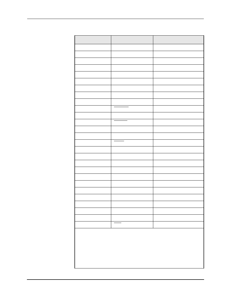
3.0 Pin Descriptions
RC224ATL/224ATLV
EmbeddedModem Family
3-12
Conexant
D224ATLVDSC
27
RFILO
--
28
AGCIN
--
29
VC
--
30
AGND
AGND
31
NC
--
32
NC
--
33
NC
--
34
NC
--
35
NC
--
36
TLKRELAY
DO
37
AGND
AGND
38
OHRELAY
DO
39
NC
--
40
NC
--
41
SLEEPI
DI
42
RAGCI
MI to RAGCO
43
AGND
AGND
44
RSTBI
MI to RSTBO
45
RRSTI
MI to RRSTO
46
RADCO
MI to RADCI
47
TDACI
MI to TDACO
48
TRSTI
MI to TRSTO
49
TSTBI
MI to TSTBO
50
NC
--
51
NC
--
52
2
DI
53
TEST
(5)
Table 3-4. RC224ATL/224ATLV 100-Pin PQFP Pin Assignments--Parallel (2 of 4)
Pin Number
Signal Label
I/O Type
(1)
NOTE(S):
(1)
I/O Types are described in
Figure 7-5, Digital Interface Characteristics
and
Figure 7-6, Analog Interface Characteristics
.
(2)
MI = Modem Interconnection.
(3)
NC = No external connection (may have internal connection, leave pin disconnected
(open)).
(4)
AGND is analog ground and DGND is digital ground.
(5)
Connect to VCC through 4.7 k
.
(6)
Connect ATL to + 5 VCC, ATLV to + 3 VCC.
RC224ATL/224ATLV
3.0 Pin Descriptions
EmbeddedModem Family
D224ATLVDSC
Conexant
3-13
54
XTLI
IE
55
XTLO
OE
56
NC
--
57
DGND
DGND
58
DGND
DGND
59
NC
--
60
NC
--
61
HD0
DIO
62
HD1
DIO
63
HD2
DIO
64
HD3
DIO
65
NMI
(6)
66
DGND
DGND
67
NC
--
68
HD4
DIO
69
HD5
DIO
70
HD6
DIO
71
HD7
DIO
72
RING
DI
73
NC
--
74
HRD
DI
75
HWT
DI
76
HCS
DI
77
NVRCS
DO
78
HA2
DI
79
(A/A1)
DO
80
DGND
DGND
Table 3-4. RC224ATL/224ATLV 100-Pin PQFP Pin Assignments--Parallel (3 of 4)
Pin Number
Signal Label
I/O Type
(1)
NOTE(S):
(1)
I/O Types are described in
Figure 7-5, Digital Interface Characteristics
and
Figure 7-6, Analog Interface Characteristics
.
(2)
MI = Modem Interconnection.
(3)
NC = No external connection (may have internal connection, leave pin disconnected
(open)).
(4)
AGND is analog ground and DGND is digital ground.
(5)
Connect to VCC through 4.7 k
.
(6)
Connect ATL to + 5 VCC, ATLV to + 3 VCC.

3.0 Pin Descriptions
RC224ATL/224ATLV
EmbeddedModem Family
3-14
Conexant
D224ATLVDSC
81
DGND
DGND
82
NC
--
83
HA1
DI
84
HA0
DI
85
IDLENO
DI
86
NVRSK
DO
87
RESET
IC
88
VCC
(6)
89
VCC
(6)
90
NC
--
91
HINT
DO
92
HDIS
DO
93
NC
--
94
NVRDIO
DIO
95
NC
--
96
NC
--
97
DGND
DGND
98
NC
--
99
NC
--
100
NC
--
Table 3-4. RC224ATL/224ATLV 100-Pin PQFP Pin Assignments--Parallel (4 of 4)
Pin Number
Signal Label
I/O Type
(1)
NOTE(S):
(1)
I/O Types are described in
Figure 7-5, Digital Interface Characteristics
and
Figure 7-6, Analog Interface Characteristics
.
(2)
MI = Modem Interconnection.
(3)
NC = No external connection (may have internal connection, leave pin disconnected
(open)).
(4)
AGND is analog ground and DGND is digital ground.
(5)
Connect to VCC through 4.7 k
.
(6)
Connect ATL to + 5 VCC, ATLV to + 3 VCC.
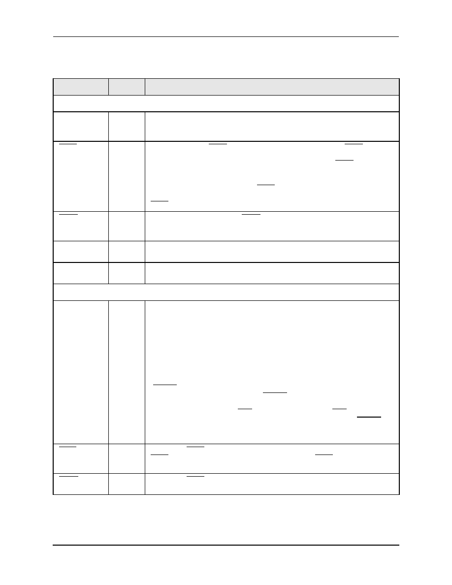
RC224ATL/224ATLV
3.0 Pin Descriptions
EmbeddedModem Family
D224ATLVDSC
Conexant
3-15
Table 3-5. Hardware Interface Signal Definitions (1 of 5)
Label
I/O Type
Signal Name/Description
System Signals
XTLI
XTLO
IE
OE
Crystal/Clock In and Crystal Out. The modem must be connected to an external crystal
circuit consisting of a 16.000312 MHz crystal and two capacitors. Alternatively, XTLI may be
driven with a buffered clock, in which case XTLO should be left open.
RESET
IC
Reset. The active low RESET input resets the internal modem logic. Upon RESET
transitioning from high to low, modem operation returns to the state controlled by factory
default values and stored values in NVRAM. During modem power-on, RESET must be held
low for at least 5 ms after +5 VD and +5 VA operating voltage (see TSVD and +5 VA below) is
attained for the modem top stabilize.
When the serial interface is selected, RESET can be connected to an external RC network
to cause the modem to reset upon power turn on. When the parallel interface is selected,
RESET should be connected to the hose bus reset line.
SEREN
DI
Serial Interface Enable. When the SEREN input is low, serial interface is selected upon reset.
In this case, the serial interface signals should be connected to the V.24 (EIA-232-D) interface
and LED indicators.
VCC
VAA
PWR
Digital Supply. +5 V/3.3V ATLV
±
5% is required.
Analog Supply. +5 V ±5% is required.
DGND
AGND
GND
Digital and Analog Grounds.
Sleep Mode Signals
IDLEN0
IDLEN1
DI
DI
Idle Enable 0 and Idle Enable 1. Encoded inputs enable or disable the sleep modes as
follows:
IDLEN1
IDLEN0 Mode
L
L
Idle mode disabled
L
H
Idle mode enabled
H
L
Stop mode disabled
H
H
Stop mode enabled
If Idle option is enabled, the modem will enter idle mode after 5 seconds of inactivity
(WAKEUP must also be high for the serial interface). The modem will wakeup upon DTE
activity (RXD for parallel mode and low on WAKEUP for serial mode) or the presence of
RING.
If Stop option is selected, the RING input becomes RING (i.e., the RING signal must be
inverted). The modem will enter stop mode after 5 seconds of inactivity (and if WAKEUP is
high for the serial interface). Only a 4 ms or longer pulse on the RING pin can wake up the
modem from stop mode.
SLEEP
DO
Sleep Mode. SLEEP output high indicates the modem is operating in its normal mode.
SLEEP low indicates that the modem is in the sleep mode. The SLEEP output can also be
used to control power to other devices.
SLEEPI
DI
Sleep Mode. SLEEP input low causes the Integrated Analog (IA) to enter low-power sleep
mode.
3.0 Pin Descriptions
RC224ATL/224ATLV
EmbeddedModem Family
3-16
Conexant
D224ATLVDSC
WAKEUP
DI
Wake Up. For serial interfaces only, WAKEUP input low removes the modem from the sleep
mode (if in the sleep mode), or prevents the modem from entering the sleep mode (if not in
the sleep mode). WAKEUP high allows the modem to enter sleep mode after 5 seconds of
modem inactivity. WAKEUP is typically connected to DTR or TXD.
NVRAM Interface
NVRCS
DO
NVRAM Chip Select. NVRCS output high enables the NVRAM.
NVRSK
DO
NVRAM Shift Clock. The NVRSK output is used to shift data to or from the NVRAM.
NVRDIO
DIO
NVRAM Data In/NVRAM Data Out. NVRDIO is a bidirectional signal that carries both the
serial input data from the NVRAM and the serial output data to the NVRAM. Depending on the
specific NVRAM used, a resistor may be required between the NVRAM DO output pin and the
modem NVRDIO bidirectional line. (Refer to
Figure 3-5
and the NVRAM data sheet.)
Speaker Interface
SPKR
O(DF)
Speaker Analog Output. The SPKR output reflects the output of the receive analog signal.
The SPKR output is turned on or off by the Speaker Control Option (Mn command), and the
gain is controlled by the Speaker Volume Option (Ln command). When the speaker is turned
off, the SPKR output is clamped to the voltage at the VC pin. The SPKR output can drive a
load as low as 300
. Typically, the SPKR output is an input to an external LM386 audio
power amplifier.
Asynchronous Serial Interface (Serial Interface Only; SEREN = Low)
RXD
DO
Received Data. The modem presents received serial data to the RXD output pin.
TXD
DI
Transmitted Data. The modem obtains serial data to be transmitted from the TXD pin.
DTR
DI
Data Terminal Ready. DTR input ON (low) indicates that the DTE is ready to operate. DTR
input OFF (high) indicates that the DTE is not ready to operate.
CTS
DO
Clear to Send. In data modes, the CTS output is ON; in fax modes, CTS is optionally used for
flow control.
DSR
DO
Data Set Ready. The DSR output is controlled by the AT&Sn command.
DCD
DO
Data Carrier Detected. The DCD output is controlled by the AT&C command.
CI/HS
DO
Calling Indicator/High Speed Indicator. CI/HS output ON (low) indicates modem connection
at 2400 bps.
RI
DO
Ring Indicator. RI output ON (low) indicates the presence of an ON segment of a ring signal
on the telephone line. (The ring signal cycle is typically 2 seconds ON, 4 seconds OFF.) The
OFF (high) condition of the RI output is maintained during the OFF segment of the ring cycle
(between rings) and at all other times when ringing is not being received.
Serial Indicator Interface (Serial Interface Only; SEREN = Low)
AAE
DO
Auto Answer Enable. AAE output ON (low) indicates that modem auto answer mode has
been enabled with the S0 = command. AAE high indicates auto answer has been disabled.
The AAE output also indicates the status of the RI output.
MR
DO
Modem Ready. MR output ON (low) indicates that the modem is ready; i.e., modem power is
on and a test mode is not selected. In a test mode, the MR output pulses to indicate a test is
in process.
Table 3-5. Hardware Interface Signal Definitions (2 of 5)
Label
I/O Type
Signal Name/Description
RC224ATL/224ATLV
3.0 Pin Descriptions
EmbeddedModem Family
D224ATLVDSC
Conexant
3-17
DCDL
DO
DCD Indicator. The DCDL output is controlled by the AT&C command.
DTRL
DO
DTR Indicator. The DTRL output is controlled by the AT&D command.
Parallel Host Interface (Parallel Interface Only)
When the HWT input signal is connected to the host bus write line, the parallel interface is
selected upon reset. (See
Section 7.3, Interface Timing and Waveforms
for waveform and
timing information.)
The parallel interface emulates a 16C450 UART; (See
Table 2-1, Parallel Interface
Registers
). Parallel interface operation is equivalent to 16C450 operation with CS0 and CS1
inputs high and DISTR, DOSTR, and ADS inputs low. The corresponding RC224ATLV and
16C450 signals are shown below. 16C450 signals that are not required for RC224ATLV host
computer operation are not shown.
16C450 Signal
RC224ATLV Signal
A0 - A2
HA0 - HA2
D0 - D7
HD0 - HD7
MR RESET (Active low)
CS2 HCS
DISTR HWT
DOSTR
HRD
INTRPT
HINT
DDIS HDIS
OUT2
None (Implemented internally in RC224ATLV)
HA0-HA2
HD0-HD7
DI
DIO
Host Bus Address Lines 0-2. During a host read or write operation, signals HA0≠HA2 select
an internal register. The state of the divisor latch access bit (DLAB) affects the selection of
certain registers.
Host Bus Data Lines 0-7. HD0-HD7 are comprised of eight tri-state I/O lines providing
bidirectional communication between the host and the modem. Data, control words, and
status information are transferred through HD0-HD7.
HCS
DI
Host Bus Chip Select. HCS input low enables reading from or writing to the modem using the
parallel bus.
HRD
DI
Host Bus Read. HRD is an active low read control input. When the modem is selected with
HCS, HRD low allows status or data words to be read from an addressed register.
HWT
DI
Host Bus Write. HWT is an active low write control input. When the modem is selected with
HCS, HWT low allows data or control words to be written to an addressed register.
Table 3-5. Hardware Interface Signal Definitions (3 of 5)
Label
I/O Type
Signal Name/Description
DLAB
HA2
HA1
HA0
Register
0
0
0
0
Receive Buffer Register (Read),
Transmitter Holding Register (Write)
0
0
0
1
Interrupt Enable Register
X
0
1
0
Interrupt Identification Register (Read Only)
X
0
1
1
Line Control Register
X
1
0
0
Modem Control Register
X
1
0
1
Line Status Register (Read Only)
X
1
1
1
Scratch Register
1
0
0
0
Divisor Latch Register (Least Significant Byte)
1
0
0
1
Divisor Latch Register (Most Significant Byte)
3.0 Pin Descriptions
RC224ATL/224ATLV
EmbeddedModem Family
3-18
Conexant
D224ATLVDSC
HDIS
DO
Host Bus Driver Disable. HDIS output is low when the host is reading data from the modem
over the host data bus (both HRD and HCS are low). HDIS is also used to disable the external
transceiver drivers whenever data is not being read from the modem.
HINT
DO
Host Bus Interrupt. HINT output is 16C450-compatible output indicating interrupt status and
is enabled by the OUT2 bit set to a 1 in the Modem Control Register.
Telephone Line Interface
TXA1
TXA2
O(DF)
Transmit Analog 1 and 2. The TXA1 and TXA2 outputs are differential outputs. A 600
telephone coupling transformer may be driven directly without the need for external discrete
buffer amplifiers.
Both TXA1 and TXA2 outputs are turned off when the transmitter is disabled or during
local analog loopback.
RXA
I(DA)
Receive Analog. RXA is a single-ended receive data input from the telephone line interface.
VC
OA
Centerpoint Voltage. A +2.5 VDC centerpoint voltage derived from an internal reference
voltage. The TXA1 and TXA2 outputs are biased at VC.
TLKRELAY
DO
Talk/Data Relay Driver. TLKRELAY is an open drain output which can directly drive a relay
with greater than 360
coil resistance and has "must operate" voltage of no greater than 4.0
VDC. A heavier load, such as an electro-mechanical relay, requires the use of an external
transistor. An external diode should be provided across the relay coil.
The TLKRELAY output is clamped off during power-on reset or the sleep mode. The
TLKRELAY output is activated and deactivated at the same time as the OHRELAY output.
In a typical application, TLKRELAY ON opens the normally closed Talk/Data relay and
disconnects the handset from the telephone line.
OHRELAY
DO
Off-Hook Relay Driver. OHRELAY is an open drain output which can directly drive a relay with
greater than 360
coil resistance and has "must operate" voltage of no greater than 4.0
VDC. A heavier load, such as an electro-mechanical relay, requires the use of an external
transistor. An external diode should be provided across the relay coil.
The OHRELAY output is clamped off during power-on reset or the sleep mode. In a typical
application, OHRELAY ON closes the normally open Off-Hook relay and connects the modem
to the telephone line (off-hook).
RING
DI
Ring Detector. RING is a TTL-compatible input used to indicate to the modem that a 15.3 Hz
to 63 Hz ringing signal is present.
The signal (a 4N35 optoisolator compatible output) into the RING input should not
respond to a voltage less than 40 V
RMS
, 15 Hz to 68 Hz, appearing across TIP and RING with
respect to ground.
A low-going edge on the RING input also removes the modem from the sleep mode.
A/A1
DO
Key Telephone Hold Indicator. A/A1 output low indicates that the telephone line is in use
when used on multi-line key telephones.
Table 3-5. Hardware Interface Signal Definitions (4 of 5)
Label
I/O Type
Signal Name/Description

RC224ATL/224ATLV
3.0 Pin Descriptions
EmbeddedModem Family
D224ATLVDSC
Conexant
3-19
Modem Interconnect
RFILO
MI
Receive Filter Output. RFILO is the output of the internal receive anti-aliasing filter which
must be connected to AGCIN through a 0.1
µ
F, 20%, DC decoupling capacitor. The 1000 pF
capacitor to ground provides noise immunity at low noise levels.
AGCIN
MI
Receive AGC Gain Amplifier Input. See RFILO.
MODEO (DSP),
MODEI (IA)
MI
Mode Control. Direct modem interconnect line.
TDACO (DSP),
TDACI (IA)
MI
Transmitter DAC Signal. Serial digital DAC signal. Direct modem interconnect line.
TSTBO (DSP),
TSTBI (IA)
MI
Transmitter Strobe. 576 kHz digital transmitter timing reference. Direct modem interconnect
line.
TRSTO (DSP),
TRSTI (IA)
MI
Transmitter Reset. 9.6 kHz, 8228.57 Hz, or 7.2 kHz digital transmitter timing reference.
Direct modem interconnect line.
RADCI (DSP),
RADCO (IA)
MI
Receiver ADC Signal. Serial digital ADC signal. Direct modem interconnect line.
RAGCO (DSP),
RAGCI (IA)
MI
Receiver AGC Signal. Serial digital AGC signal. Direct modem interconnect line.
RRSTO (DPS),
RRSTI (IA)
MI
Receiver Reset. 9.6 kHz, 8228.57 Hz, or 7.2 kHz digital receiver timing reference. Direct
modem interconnect line.
RSTBO (DSP),
RSTBI (IA)
MI
Receiver Strobe. 576 kHz digital receiver timing reference. Direct modem interconnect line.
Table 3-5. Hardware Interface Signal Definitions (5 of 5)
Label
I/O Type
Signal Name/Description
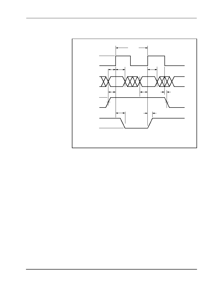
3.0 Pin Descriptions
RC224ATL/224ATLV
EmbeddedModem Family
3-20
Conexant
D224ATLVDSC
Figure 3-5. NVRAM Timing
4
µS
(1)
NVRSK
NVRDI
NVRCS
NVRDO
tDIS
0.4
µS
tDIS
0.4
µS
tPDO
2
µS
tPDO
2
µS
tCSS
0.2
µS
tCSH
0.0
µS
tDIH
0.4
µS
tDIH
0.4
µS
NOTE(S):
(1) This is the minimum NVRSK period.

D224ATLVDSC
Conexant
4-1
4
4.0 AT Commands
Each command line must start with the AT prefix and be terminated with a
carriage return (CR). Several commands may be included on one command line.
A command line may contain up to 40 characters, excluding the AT prefix and the
terminating CR. A separator is not required between data commands. A
semicolon (;) separator is required between fax commands.
AT commands are composed of 10-bit ASCII encoded asynchronous
characters. The character format in data mode is 8 data bits with no parity, or 7
data bits with even, odd, or no (two stop bits) parity, at a data rate of 19,200, 2400,
1200, or 300 bps. The character format in fax mode is 8 data bits with no parity at
19,200 bps.
Table 4-1
lists result codes and messages.
Table 4-2
summarizes the AT
command set.
Table 4-3
summarizes the fax command set.
Table 4-1. Result Codes and Messages
Digital Code
Word Code
Meaning
0
OK
Command line executed without errors
1
CONNECT
Connection at 300 bps
2
RING
Ringing signal detected
3
NO CARRIER
Carrier lost or never present
4
ERROR
Invalid command, checksum, error in
command line, or command line exceeds 40
characters
5
CONNECT 1200
Connection at 1200 bps
6
NO DIALTONE
No dial tone detected
7
BUSY
Busy signal detected
8
NO ANSWER
No silence detected when dialing a system not
providing a dial tone
10
CONNECT 2400
Connection at 2400 bps
+F4
+FCERROR
Fax carrier error
13
DATA
Connected as data modem during auto answer
15
FAX
Connected as fax modem during auto answer

4.0 AT Commands
RC224ATL/224ATLV
EmbeddedModem Family
4-2
Conexant
D224ATLVDSC
Table 4-2. AT Command Set Summary (1 of 5)
Command
Function
Default
Parameters/Description
A/
Re-execute command
--
--
A
Answer a call
--
--
AT
Command line prefix
Parameters: none
--
Attention Code. Precedes the command line except for +++
(escape) and A/ (repeat) commands.
Bn
Select CCITT or Bell Mode
Parameters: n = 0,1
n = 1
n = 0 Selects CCITT operation at 300 or 1200 bps during Call
Establishment and a subsequent connection.
n = 1 Selects BELL operation at 300 or 1200 bps during Call
Establishment and a subsequent connection.
Cn
Carrier control
Parameters: n = 0,1
n = 1
--
D
--
--
Dial Command. D causes the modem to dial the number which
follows the D in the command line. Valid dial characteristics are 0
to 9, A to D, #, and *. Other valid dial modifier characters are ","
P, R, S=n, T, W, ";", @, and !.
Dn
Dial modifier
--
--
En
Command echo
Parameters: n = 0,1
n = 1
n = 0 Disables
command
echo.
n = 1 Enables
command
echo.
Fn
On-line character echo option
Parameters: n = 0,1
n = 1
n = 0 Returns
ERROR result code.
n = 1 Returns OK result code.
Hn
Disconnect (hang-up)
Parameters: n = 0,1
n = 0
n = 0 Modem on-hook (relay open).
n = 1 Modem off-hook (relay closed).
In
Identification
Parameters: n = 0,1,2,3
n = 0
n = 0 Reports
product
identification
code.
n = 1 Calculates the ROM checksum.
n = 2 Calculates the ROM checksum and compares it with the
prestored checksum. Reports "OK" if the calculated
checksum equals the prestored checksum or if the
prestored checksum value is FFh; otherwise reports
"ERROR".
n = 3 Reports the firmware version and ROM part number.
Ln
Speaker volume
Parameters: n = 0,1,2,3
n = 2
n = 0 Low
volume.
n = 1 Low volume.
n = 2 Medium
volume.
n = 3 High
volume.
Mn
Speaker control
Parameters: n = 0,1,2,3
n = 1
n = 0 Speaker is always off.
n = 1 Speaker is on during Call Establishment, but off when
receiving carrier.
n = 2 Speaker is always on.
n = 3 Speaker is on after dialing, until carrier is detected.
On
Go on-line
Parameters: n = 0,1
--
n = 0 On-line
state.
n = 1 On-line state with equalizer retrain.
P
Force pulse dialing
--
--
Qn
Quiet Result codes control
n = 0
n = 0 Enables result codes to the DTE.
n = 1 Disables result codes to the DTE.

RC224ATL/224ATLV
4.0 AT Commands
EmbeddedModem Family
D224ATLVDSC
Conexant
4-3
Sn
Select S register as default
Range: n = 0-27
--
n
Establishes S-Register n as the last register accessed.
n = v
Sets S-Register n to the value v.
n?
Reports the value of S-Register n.
Sn =
Parameters: none
Range:
n = 0-27 (register
no.)
x=0-255 (value)
--
Writes to an S Register. Sr=x sets register "n" to the value "x".
Configuration registers are provided to retain modem
configuration parameters. The contents of these registers can be
modified with this command.
Sn?
Parameters: none
Range: n = 0-27
--
Reads an S register. Sn? causes the contents stored in register
"n" to be returned.
T
Force DTMF dialing
--
--
Vn
Report codes form
n = 1
n = 0 Result code is sent as a digit.
n = 1 Result code is sent as ASCII text.
Xn
Extended result codes
n = 4
n = 0 Basic set of result codes 0-4 are enabled. The modem
blind dials and sends the appropriate connect result code
once a satisfactory connection is established. Dial tone
and busy are not recognized.
n = 1 Result codes 0-5 and 10 are enabled. The modem blind
dials and sends the appropriate connect result code once
a satisfactory connection is established. Dial tone and
busy are not recognized.
n = 2 Result codes 0-6 and 10 are enabled; dial tone detected.
The modem waits for a dial tone before dialing, then
sends the appropriate result code once a satisfactory
connection is established. The busy result code is sent if
a busy signal is detected.
n = 3 Result codes 0-5, 7 and 10 are enabled; busy signal
detected; dial tone not detected. The modem blind dials
and sends the appropriate connect result code once a
satisfactory connection is established. The busy result
code is sent if a busy signal is detected.
n = 4 Result codes 0-7 and 10 are enabled; busy signal and
dial tone detected. The modem waits for a dial tone
before dialing, then sends the appropriate result code
once a satisfactory connection is established. The NO
DIALTONE result code is sent if the dial tone is not
detected within 5 seconds. The BUSY result code is sent
if a busy signal is detected.
Yn
Long space disconnect
n = 0
n = 0 Disables long space disconnect.
n = 1 Enables long space disconnect.
Zn
Soft reset and restore profile
n = 0
n = 0 Soft reset. Restores stored profile 0.
n = 1 Soft reset. Restores stored profile 1.
&Cn
RLSD (DCD) option
n = 0
n = 0 RLSD remains ON at all times.
n = 1 RLSD follows the state of the carrier.
Table 4-2. AT Command Set Summary (2 of 5)
Command
Function
Default
Parameters/Description

4.0 AT Commands
RC224ATL/224ATLV
EmbeddedModem Family
4-4
Conexant
D224ATLVDSC
&Dn
DTR option
n = 0
n = 0 Modem
ignores
DTR.
n = 1 Modem assumes command state when ON-to-OFF
transition is detected on DTR.
n = 2
Modem hangs up, assumes command state and disables
auto-answer upon detecting ON-toOFF transition on
DTR.
n = 3 Modem assumes software reset state upon detecting
ON-to-OFF transition on DTR.
&F
Recall (restore) factory profile
--
S Registers: S0=1, S1=0, S2=43. S3=13, S4=10, S5=8, S6=0,
S7=30, S8=2, S9=5, S10=14, S11=95, S12=50, S18=0, S25=5,
S26=1
Commands: B1, C1, E1, F1, L2, M1, P, Q0, V1, Y0, X4, &C0, &D0,
&G0, &J0, &M0/&G0, &P0, &R0, &S0, &T4, &X0
&Gn
Select guard tone
n = 0
n = 0 No guard tone.
n = 1 550 Hz guard tone.
n = 2 1800 Hz guard tone.
&Jn
Telephone jack control
n = 0
n = 0 Suitable for RJ11, RJ41S. or RJ45S type phone jack.
n = 1 Suitable for RJ12 or RJ13 type phone jack; the A lead is
connected to A1 lead while the modem is off-hook.
&L0
Dial-up line operation
n = 0
n = 0 Requests
dial-up
operation.
&Mn
Asynchronous mode
n = 0
n = 0 Asynchronous
operation.
n = 1 Reserved
n = 2 Reserved
n = 3 Reserved
&Pn
Pulse dial make/break ratio
n = 0
n = 0 Selects 39%≠61% make/break ratio at 10 pps.
(USA/Canada)
n = 1 Selects 33%≠67% make/break ratio at 10 pps. (UK/HK)
&Q0
Asynchronous mode
n = 0
Idle State On-line State
n = 0 Normal Asynchronous
n = 1 Reserved Reserved
n = 2 Reserved Reserved
n = 3 Reserved Reserved
&Sn
DSR override
n = 0
n = 0 DSR will remain ON at all times.
n = 1 DSR will become active after answer tone has been
detected and inactive after the carrier has been lost. DSR
is OFF when the modem is in test mode or idle state.
Table 4-2. AT Command Set Summary (3 of 5)
Command
Function
Default
Parameters/Description

RC224ATL/224ATLV
4.0 AT Commands
EmbeddedModem Family
D224ATLVDSC
Conexant
4-5
&Tn
Test and diagnostic
n = 4
n = 0 Terminates test in progress.
n = 1 Initiates local analog loopback.
n = 2 Returns
ERROR.
n = 3 Initiates
local
digital
loopback.
n = 4 Enables digital loopback acknowledgment from remote
modem for RDL.
n = 5 Disables digital loopback acknowledgment from remote
modem for RDL.
n = 6 Initiates
remote
digital
loopback.
(1)
n = 7 Initiates remote digital loopback with self test.
(1)
n = 8 Initiates local analog loopback with self test.
(1)
&V
Display current configurations
--
Example:
AT&V
ACTIVE PROFILE:
B0 E1 L1 M1 QO T V1 Y0 &C0 &D0 &G2 &J0 &L0 &P0 &Q0 &R0
&S0 &X0 &Y0
S00:000 S01:000 S02:043 S03:013 S04:010 S05:008 S06:002
S07:030 S08:002 S09:006
S10:014 S12:050 S14:AAH S16:00H S18:000 S21:00H S22:76H
S23:17H S25:005 S26:001 S27:40H
STORED PROFILE 0:
B1 E1 L2 QO V1 X4 Y0 &C0 &D0 &G0 &J0 &L0 &P0 &Q0 &R0
&S0 &X0
S00:000 S14:AAH S18:000 S21:00H S22:76H S23:17H S25:005
S26:001 S27:40H
STORED PROFILE 1:
B1 E1 L2 QO V1 X4 Y0 &C0 &D0 &G0 &J0 &L0 &P0 &Q0 &R0
&S0 &X0
S00:000 S14:AAH S18:000 S21:00H S22:76H S23:17H S25:005
S26:001 S27:40H
TELEPHONE NUMBERS:
&Z0= 5551212
&Z1=
&Z2=
&Z3=
&Wn
Store current configuration
n = 0
Commands: Bn, En, Ln, Mn, P or T, Qn, Vn, Yn, &Cn &Dn, &Gn,
&Jn, &Ln, &Pn, &Qn, &Rn, &Sn &Xn &Yn
Registers: S0, S1, S2, S3, S4, S5, S6, S7, S8, S9, S10, S12,
S14, S16, S18, S21, S22, S23, S25, S26, S27
n = 0 Stores active profile in location 0.
n = 1 Stores active profile in location 1.
&X0
Asynchronous data
transmission
n = 0
n = 0 Reserved
n = 1 Reserved
n = 2 Reserved
&Yn
Select default profile
--
n = 0 The modem will use profile 0 on powerup.
n = 1 The modem will use profile 1 on powerup.
&Zn = x
Store dial string to location n
--
&Zn = x n = 0 to 3 and x = dial string. (up to 36 characters)
Table 4-2. AT Command Set Summary (4 of 5)
Command
Function
Default
Parameters/Description

4.0 AT Commands
RC224ATL/224ATLV
EmbeddedModem Family
4-6
Conexant
D224ATLVDSC
%Dn
DTMF Level Attenuation
--
--
%J
Load Secondary Defaults
--
--
%Ln
Transmit Level Attenuation
--
--
Dial
Modifier
Function
P
Pulse Dial
Parameters: none
--
--
R
Originate Call in Answer Mode
Parameters: none
--
--
S=n
Dial Stored Number
Parameters:
n = 0, 1, 2, 3
S<CR>
S=<CR>
S=n<CR> where n = 0-3
--
--
T
Tone Dial
Parameters: none
--
--
W
Wait for Dial Tone
Parameters: none
--
--
;
Return to Idle State
Parameters: none
--
--
@
Wait for Quiet Answer
Command
Parameters: none
--
--
!
Flash Hook
Parameters: none
--
--
, (comma)
Pause
Parameters: none
--
--
0-9, A, B, C,
D, #, *
Dial Digits/Characters
Parameters: none
--
--
NOTE(S):
(1)
Not available for 300 bps.
Table 4-2. AT Command Set Summary (5 of 5)
Command
Function
Default
Parameters/Description

RC224ATL/224ATLV
4.0 AT Commands
EmbeddedModem Family
D224ATLVDSC
Conexant
4-7
Table 4-3. Fax Command Set Summary (1 of 2)
Fax Command
Function
Default
Parameters/Description
+FCLASS=n
Service class
n = 0
Select Service Class. +FCLASS=n command sets the active service
class.
+FCLASS=0
Returns to data mode
+FCLASS=1
Fax Class 1
+FCLASS=2
Fax Class 2 (Not supported)
+FCLASS=3
Fax Class 3 (Not supported)
+F<command>?
Report Active Configuration
--
Report Active Configuration. +F<command>? interrogates the
modem to determine the active configuration.
The responses are:
+FAA?
0 if auto answer is disabled; 1 if auto answer is
enabled
+FCLASS
0 if in data mode; 1 if in fax class 1
+FF?
0 if flow control off; 1 if flow control on
+F<command>=?
Report Operating
Capabilities
--
Report Operating Capabilities. +F<commands>=? can be used to
determine the operating capabilities of the modem.
The responses are:
+FAA=?
0, 1
+FCLASS=? 0, 1
+FTM=?
24, 48, 72, 96
+FTM=?
24, 48
+FTH=?
3
+FTH=?
3
+FF=?
0,1
+FAA=n
Data/Fax Auto Answer
n = 0
Data/Fax Auto Answer. +FAA command configures the modem to
automatically detect whether an incoming call is from a data
modem or a fax modem. This command is valid in both data and
fax modes.
n = 0 Disable data/fax auto answer mode (default).
n = 1 Enable data/fax auto answer mode. The modem
determines calling type and issues DATA result code (13) if
caller is a data modem, or issues FAX result code (15) in
the caller is a fax modem.
+FF
Enhanced Flow Control
n = 0
Enhanced Flow Control. +FF=n command enables an enhanced
flow control mode for data transfer between the DTE and DCE.
n = 0
Disables enhanced flow control interface. In this mode,
data transfer is compatible with the EIA-578 standard.
n = 1 Enables enhanced flow control.
+FTS=n
Stop Transmission and Wait
n = 0
Stop Transmission and Wait. +FTS=n causes the modem to
terminate a transmission. After temination the modem waits for n
10≠ms intervals before responding with the OK result code. An
ERROR response code results if this command is issued while the
modem is on-hook.
+FRS=n
Receive Silence
n = 0
Receive Silence. +FRS=n causes the modem to report back to the
DTE with an OK result code after n 10-millisecond intervals of
silence have been detected on the line. This command is aborted if
any command character is received. The modem discards the
aborting character and issues an OK result code. An ERROR
response code results if this command is issued while the modem
is on-hook.

4.0 AT Commands
RC224ATL/224ATLV
EmbeddedModem Family
4-8
Conexant
D224ATLVDSC
+FTM=n
Transmit Data
n = 48
Transmit Data. +FTM=n causes the modem to transmit data using
the modulation defined below. An ERROR response code results if
this command is issued while the modem is on-hook.
+FTM=24
V.27 ter 2400 bps
+FTM=48
V.27 ter 4800 bps
+FTM=72
V.29 7200 bps
+FTM=96
V.29 9600 bps
+FRM=n
Receive Data
n = 48
Receive Data. +FRM=n causes the modem to enter the receiver
mode using the modulation defined below. An ERROR response
code results if this command is issued while the modem is
on-hook.
+FRM=24
V.27 ter 2400 bps
+FRM=48
V.27 ter 4800 bps
+FRM=72
V.29 7200 bps (Not supported
(1)
)
+FRM=96
V.29 9600 bps (Not supported
(1)
)
+FTH=n
Transmit Data with HDLC
Framing
n = 3
Transmit Data with HDLC Framing. +FTH=n causes the modem to
transmit data framed in HDLC protocol using the modulation
defined below. An ERROR response code results if this command
is issued while the modem is on-hook.
+FTH=3
V.21 Channel 2300 bps
+FRH=n
Receive Data with HDLC
Framing
n = 0
Receive Data with HDLC Framing. +FRH=n causes the modem to
receive frames in HDLC protocol using the modulation defined
below. An ERROR response code results if the command is issued
while the modem is on-hook.
+FRH=3
V.21 Channel 2300 bps
+FRTn
Receive Test Data
n = 48
Receive Test Data. +FRTn causes the modem to go off-hook and
begin demodulating received data at the specified rate.
n
Configuration/Data Rate
n = 24
V.27 ter 2400 bps
n = 48
V.27 ter 4800 bps
+FTTn = m
Transmit Test Data
n = 96
m = 0
Transmit Test Data. +FTTn = m causes the modem to transmit a
continuous test pattern at the specified rate. The transmission will
terminate by a DTE abort (i.e., any character recognized at the DTE
interface).
n
Configuration/Data Rate
n = 24
V.27 ter 2400 bps
n = 48
V.27 ter 4800 bps
n = 72
V.29 7200 bps
n = 96
V.29 9600 bps
m
Test Pattern
m = 0
ASCII data (20h - 7Fh sequential)
m = 1
All zeros
m = 2
All ones
m = 3
Alternate 10
m = 4
Sliding 0 (01111)
m = 5
Sliding 1 (00001)
NOTE(S):
(1)
Modem will respond with ERROR result code.
Table 4-3. Fax Command Set Summary (2 of 2)
Fax Command
Function
Default
Parameters/Description

D224ATLVDSC
Conexant
5-1
5
5.0 S Registers
The S register commands are summarized in
Table 5-1
. The range of possible
values and the factory default value for each S register are also shown. The
factory default values are used whenever the &F command is received or a parity
error is detected in the NVRAM upon modem power turn-on.
The user-defined S registered default values are used at modem power turn-on
or when a modem reset is received. If the NVRAM is not available or contains a
parity error, the factory default S register values are used.
The S registers are described in
Table 5-2
.
Reading an S Register
The command Sn? reads the current value of an S register, where "n" is the
decimal number of the register.
Example: To read the current value in register S0 (Ring to Answer On) and S7
(Wait Time for Data Carrier), perform the following:
Enter: AT S0? S7? (Value in register S0? Value in register S7?)
A typical response to the might be:
Result: 001 (modem will answer on first ring)
Result: 030 (modem will wait 30 seconds for a carrier)
Result: OK (command completed)

5.0 S Registers
RC224ATL/224ATLV
EmbeddedModem Family
5-2
Conexant
D224ATLVDSC
Table 5-1. S Register Summary
Register
Range
Units
Default
Description
S0
(1)
0≠255
Rings
00
Rings to Auto-Answer
S1
0≠255
Rings
00
Ring Counter
S2
0≠127
ASCII
43
Escape Character
S3
0≠127
ASCII
13
Carriage Return Character
S4
0≠127
ASCII
10
Line Feed Character
S5
0≠32, 127
ASCII
08
Backspace Character
S6
2≠255
Seconds
02
Maximum time to Wait for Dial Tone
S7
1≠255
Seconds
30
Wait for Carrier
S8
0≠255
Seconds
02
Pause Time for Comma
S9
1≠255
1/10 seconds
06
Carrier Detect Response Time
S10
1≠255
1/10 seconds
14
Carrier Loss Disconnect Time
S11
50≠255
ms
95
DTMF Dialing Speed
S12
0≠255
1/50 seconds
50
Escape Prompt Delay
S14
(1)
Bit Mapped
None
AA hex
General Bit Mapped Options
S16
Bit Mapped
None
00
Test Mode Bit Mapped Options (&T)
S17
0≠250
4 ms increments
00
Fax Mode Null Byte Timer
S18
(1)
0≠255
Seconds
00
Test Timer
S19
0≠1
None
00
Conexant Protocol Interface Speed
S20
0≠127
Seconds
00
Fax Mode Inactivity Timer
S21
(1)
Bit Mapped
None
00
General Bit Mapped Options
S22
(1)
Bit Mapped
None
76 hex
General Bit Mapped Options
S23
(1)
Bit Mapped
None
07
General Bit Mapped Options
S24
0≠255
Seconds
00
Sleep Inactivity Timer
S25
(1)
0≠255
0.1 or 1 seconds
05
Delay to DTR Off
S26
(1)
0≠255
0.01 seconds
1
RTS-to-CTS Delay
S27
(1)
Bit Mapped
None
40 hex
General Bit Mapped Options
S28
(1)
Bit Mapped
None
00
General Bit-Mapped Options
NOTE(S):
(1)
Register value may be stored in one of two user profiles with the AT&W command.

RC224ATL/224ATLV
5.0 S Registers
EmbeddedModem Family
D224ATLVDSC
Conexant
5-3
Table 5-2. S Register Description (1 of 8)
Register
Default
Range
Units
Description
S0
00
0≠255
Rings
Ring to Answer On. Assigning S0 a value from 1 to 255 places the
modem in auto-answer mode. The modem will auto answer after
the specified number of rings has occurred.
Setting S0 to 0 disables auto-answer.
S1
00
0≠255
Rings
Ring Count. S1 is incremented each time a ring is detected. It will
be cleared if no ring occurs within 8 seconds after the last ring.
S2
43
0≠127
ASCII
Escape Code Character. S2 holds the ASCII value used for the
escape code. The + character responds to the factory default value.
Values greater than 127 disable the escape code operation. To
enter the command mode when the escape code is disabled, a loss
of carrier must occur or DTR must be set to a 0 (dependent on &D
command).
S3
13
0
≠
127
ASCII
Carriage Return Character. S3 holds the ASCII value for the
carriage return; 13 is the standard value. The character in S3 is
both the command line terminator and the result code terminator.
S4
10
0
≠
127
ASCII
Line Feed Character. S4 holds the ASCII value for the line feed.
The line feed character is output after the carriage return only
when English word result codes have been selected (V1). If a line
feed character is not desired, it may be changed to a null, but it
cannot be totally disabled.
S5
08
0
≠
32, 127
ASCII
Backspace Character. S5 holds the ASCII value for the backspace
character. This character is both the backspace key and the
character echoed to move the cursor back one position. Normally
a value of 8 is used. The backspace character must not be set to a
value corresponding to a printable ASCII character (i.e., between
33 and 126) or to a value greater than 127. A backspace is used as
follows:
The keystroke is echoed back to the terminal and the cursor moved
back over the last character entered. The last character in the com-
mand buffer is deleted.
S6
02
2
≠
255
Seconds
Wait for Dial Tone. S6 specifies the wait time before dialing. The
delay allows time for the dial tone to occur on the telephone line.
The minimum time is 2 seconds. Values greater than 2 seconds
may be necessary if trouble is encountered getting dial tones.
S7
30
1
≠
255
Seconds
Wait for Carrier After Dial. S7 specifies the delay time that the
modem waits for the carrier signal from the remote modem before
hanging up. Typically, a delay time of 30 seconds is enough, but it
can be extended to 255 seconds. If the carrier is not detected
within the specified time period, the modem hangs up and sends
the NO CARRIER result code. If carrier is detected, the modem
returns the CONNECT result code and goes on-line.

5.0 S Registers
RC224ATL/224ATLV
EmbeddedModem Family
5-4
Conexant
D224ATLVDSC
S8
02
0
≠
255
Seconds
Pause Time for the Comma Dial Modifiers. S8 sets the pause
time for the comma dial modifier. The comma is used during
dialing when it is necessary to dial through a PBX and wait for a
second dial tone. A 2-second delay is usually enough. S8 can be
changed or multiple commas can be used to lengthen the delay.
S9
06
1
≠
255
1/10
seconds
Carrier Detect Response Time. S9 sets the carrier detect
response time.
S10
14
1
≠
255
1/10
seconds
Lost Carrier to Hang Up Delay. S10 sets the delay time between
loss of carrier and hang-up. The modem will not hang-up due to
loss of carrier if the value of S10 is 255.
S11
95
50
≠
255
ms
DTMF Dialing Speed. S11 sets the duration and inter-digit delay
of the touch-tones.
S12
50
0
≠
255
1/50
seconds
Escape Code Guard Time. S12 sets the escape code guard time.
S13
--
--
--
Reserved
S14
AAh
Bit Mapped
None
General Bit Mapped Options. S14 is the modem option register
with the following bit functions.
Bit 0
Reserved
Bit 1
Command Echo (See E command)
0
E0≠No echo
1
E1
--
Echo (factory default)
Bit 2
Results Code (See Q command)
0
Q0
--
Enabled (factory default)
1
Q1
--
Disabled
Bit 3
Verbose Command (See V command)
0
V0
--
Digits
1
V1
--
Words (factory default)
Bit 4
Reserved
Bit 5
(1)
Dial Method (See T and P commands)
0
T
--
Tone dial
1
P
--
Pulse dial (factory default)
Bit 6
Reserved
Bit 7
Originate/Answer (See A, D, and R commands, and
register S0)
0
Answer
1
Originate (factory default)
S15
--
--
--
Reserved
Table 5-2. S Register Description (2 of 8)
Register
Default
Range
Units
Description

RC224ATL/224ATLV
5.0 S Registers
EmbeddedModem Family
D224ATLVDSC
Conexant
5-5
S16
00
--
None
Modem Test Option. Controls the diagnostic modes as follows:
Bit 0
Local Analog Loopback L3 (See &T1 command)
0
Disabled (factory default)
1
&T1
--
Enabled
Bit 1
Reserved
Bit 2
Local Digital Loopback (See &T3 command)
0
Disabled (factory default)
1
&T3
--
Enabled
Bit 3
Remote Digital Loopback L2 (See &T6 command)
0
Disabled (factory default)
1
&T6
--
Enabled
S17
00
0-250
4 ms
Increments
Fax Mode Null Byte Timer. The value of S17 determines the
length of time null bytes are sent by the modem if the last byte
sent during DTE underrun in Fax Mode is not a null byte.
0
S17
250 corresponds to a timer value of 0≠1 second (i.e.,
the timer value is the value of S17 times 4 ms).
S18
00
0-255
Seconds
Test Timer. Sets the length of time the modem conducts a test
before returning to the command mode. If this register is zero, the
test will not automatically terminate; the test must be terminated
from the command mode by issuing an AT&T0 or ATH command.
S19
--
--
--
Not Supported
S20
0
1-127
Seconds
Fax Mode Inactivity Timer. S20 can be used to cause the modem
to automatically place the telephone on-hook or reset itself if
inactivity (of variable duration) is detected while in Fax Mode.
Table 5-2. S Register Description (3 of 8)
Register
Default
Range
Units
Description

5.0 S Registers
RC224ATL/224ATLV
EmbeddedModem Family
5-6
Conexant
D224ATLVDSC
S21
00
Bit Mapped
--
Bit Mapped Options. S21 is the modem register with the following
bit functions:
Bit 0
Telco Jack (See &J Command)
0
&J0
--
11/RJ-45S (factory default)
1
&J1
--
RJ-12/RJ-13
Bit 1
Reserved
Bit 2
Ready to Send (RTS)/Clear to Send (CTS). (See &R
Command)
0
&R0
--
CTS tracks RTS (not supported)
1
&R1
--
RTS is ignored (factory default)
Bit 3, 4
Data Terminal Ready (DTR) (See &D Command)
4 3
0 0
&D0
--
Modem ignores DTR (factory default)
0 1
&D1
--
Modem goes to command state if
ON-to-OFF transition on DTR
1 0
&D2≠Modem "hangs up" if ON-to-OFF
transition on DTR
1 1
&D3
--
Modem goes to initialization state if
ON-to-OFF transition on DTR
Bit 5
Data Carrier Detect (DCD) (See &C Command)
0
&C0
--
DCD is always on (factory default)
1
&C1
--
An ON condition on DCD indicates the
presence of a valid data carrier
Bit 6
Data Set Ready (DSR) (See &S Command)
0
&S0
--
DSR is always on
1
&S1
--
DSR is turned on at the start of
handshaking
Bit 7
Long Space Disconnect (See Y Command)
0
&Y0
--
Disabled (factory default)
1
&Y1
--
Enabled
Table 5-2. S Register Description (4 of 8)
Register
Default
Range
Units
Description

RC224ATL/224ATLV
5.0 S Registers
EmbeddedModem Family
D224ATLVDSC
Conexant
5-7
S22
76h
Bit Mapped
--
Bit Mapped Options. S22 is the modem register with the following
bit functions:
Bit 0, 1
Speaker Volume (See L Command)
1 0
0 0
L0
--
Speaker volume low
0 1
L1
--
Speaker volume low
1 0
L2
--
Speaker volume medium (factory default)
1 1
L3
--
Speaker volume high
Bit 2, 3
Speaker Control (See M Command)
3 2
0 0
M0
--
Speaker disabled
0 1
M1
--
Speaker on until carrier detected (factory
default)
1 0
M2
--
Speaker always on
1 1
M3
--
Speaker on until carrier detected but off
during dialing
Bit 4, 5, 6Result Code Options (See X Command)
6 5 4
0 0 0
X0
--
Selects appropriate connect result code,
goes off-hook when the dial command is
received, waits the number of nds given by
register S6, and "blind dials" (does not look
for dial tone).
0 0 1
Reserved
0 1 0
Reserved
0 1 1
Reserved
1 0 0
X1
--
Selects appropriate connect result code,
goes off-hook, waits the number of seconds
specified by register S6 and blind dials
without waiting for dial tone. Busy is not
detected.
1 0 1
X2
--
Selects appropriate connect result code,
goes off-hook, and dials when dial tone is
detected. Busy is not detected.
1 1 0
X3
--
Selects appropriate connect result code,
goes off-hook, waits the number of seconds
specified in register S6, blind dials, detects
busy signal and sends BUSY result code.
1 1 1
X4
--
Selects appropriate connect result code,
goes off-hook and dials when dial tone is
detected, detects busy signal and sends BUSY
result code. All result codes are enabled
(factory default).
Bit 7
Make/Break Ratio (See &P Command)
0
&P0
--
39/61 United States/Canada (factory
default)
1
&P1
--
33/67 UK/Hong Kong
Table 5-2. S Register Description (5 of 8)
Register
Default
Range
Units
Description
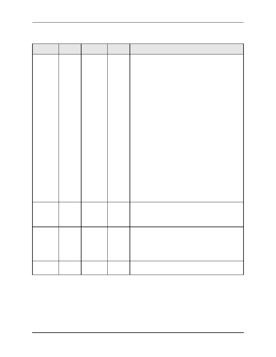
5.0 S Registers
RC224ATL/224ATLV
EmbeddedModem Family
5-8
Conexant
D224ATLVDSC
S23
07
Bit Mapped
--
Bit Mapped Options.
Bit 0
Obey request from remote modem for a Remote Digital
Loopback (See &T4 and &T5 Commands)
0
&T5 selected
--
RDL disabled
1
&T4 selected
--
RDL enabled (factory default)
Bit 1, 2
Communications Rate
2 1
0 0
300 bps
0 1
Reserved
1 0
1200 bps
1 1
2400 bps (factory default)
Bit 3
Reserved
Bit 4, 5
Parity Option
5 4
0 0
Even parity (factory default)
0 1
Space parity
1 0
Odd parity
1 1
Mark/None parity
Bit 6, 7
Guard Tones (See &G Command)
7 6
0 0
&G0
--
Guard tone disabled (factory default)
0 1
Reserved
1 0
&G2
--
1800 Hz guard tone
1 1
Reserved
S24
00
0-255
Seconds
Sleep Mode Inactivity Timer. S24 is used to set the amount of
time the modem may be inactive before it will enter sleep mode.
The range of S24 is 0
S24
4, and Sleep Mode is inhibited when
S24 = 255. (Also see Sleep Mode Signals in
Table 3-5
.)
S25
05
0-255
0.01 or 1
Seconds
Detect DTR Change. If &Q1 is selected, S25 is the delay in
seconds after a connection has been made, but before the modem
examines the DTR lead.
If in the on-line or on-line command state, changes in DTR that last
less than the time specified by S25, in 0.01 sec increments, are
ignored by the modem.
S26
01
0-255
0.01
Seconds
RTS to CTS Delay Intervals. Reserved
Table 5-2. S Register Description (6 of 8)
Register
Default
Range
Units
Description

RC224ATL/224ATLV
5.0 S Registers
EmbeddedModem Family
D224ATLVDSC
Conexant
5-9
S27
40h
Bit Mapped
--
Bit Mapped Options.
Bit 3, 1, 0Communications Mode Option (See &D Command)
3 1 0
0 0 0
&Q0 selected
--
Asynchronous (factory
default)
0 0 1
&Q1 selected
--
Synchronous (not supported)
0 1 0
&Q2 selected
--
Synchronous (not supported)
0 1 1
&Q3 selected
--
Synchronous (not supported)
1 0 0
Reserved
1 0 1
Reserved
1 1 0
Reserved
1 1 1
Reserved
Bit 2
Dial Up/Leased Line Option
0
Dial Up (factory default)
1
Leased Line (not supported)
Bit 4, 5
Synchronous Transmit Clock Source Selection (See &X
Command)
5 4
0 0
&X0
--
Internal Clock (factory default)
0 1
&X1
--
External DTE Clock (not supported)
1 0
&X2
--
Receive Clock (not supported)
1 1
Reserved
Bit 6
Communications Standard Option (See B Command)
0
B0
--
CCITT V.22 bis/V.22
1
B1
--
Bell 212A (factory default)
Bit 7
Data/Fax Discrimination (i.e., AT+FAA Status)
0
Data/Fax auto answer mode disabled
(AT+FAA = 0)
1
Data/Fax auto answer mode enabled
(AT+FAA = 1)
Table 5-2. S Register Description (7 of 8)
Register
Default
Range
Units
Description

5.0 S Registers
RC224ATL/224ATLV
EmbeddedModem Family
5-10
Conexant
D224ATLVDSC
S28
00
Bit Mapped
--
Bit Mapped Options.
Bit 2, 1, 0Transmit Level Attenuation (See %Ln Command)
2 1 0
Description
0 0 0
0 dB attenuation
0 0 1
2 dB attenuation
0 1 0
4 dB attenuation
0 1 1
6 dB attenuation
1 0 0
8 dB attenuation
1 0 1
10 dB attenuation
1 1 0
12 dB attenuation
1 1 1
14 dB attenuation
Bit 5, 4, 3DTMF Transmit Level Attenuation (See %Dn Command)
5 4 3
Description
0 0 0
0 dB attenuation
0 0 1
2 dB attenuation
0 1 0
4 dB attenuation
0 1 1
6 dB attenuation
1 0 0
8 dB attenuation
1 0 1
10 dB attenuation
1 1 0
12 dB attenuation
1 1 1
14 dB attenuation
Bit 6
Dialing Pulses per Second
0
10 pps
1
20 pps
Bit 7
Secondary Defaults (See %J Command)
0
&F defaults
1
%J defaults
NOTE(S):
(1)
Bit 5 is set or reset if the dial command string contains a P (pulse dial) or T (tone dial), respectively. If a subsequent dial
command string is used with a P or T, the modem uses the option specified by this bit.
Table 5-2. S Register Description (8 of 8)
Register
Default
Range
Units
Description
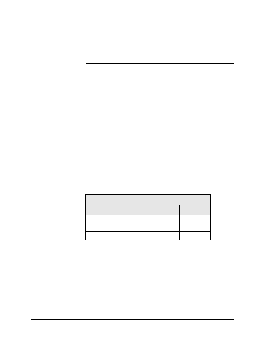
D224ATLVDSC
Conexant
6-1
6
6.0 Operation
Modem operation supports data modem processing, fax modem processing and
common call progress processing.
The AT+FCLASS command allows the operator to select either data or fax
operation.
AT+FCLASS=0 Data mode
AT+FCLASS=1 Fax mode Class 1
6.1 Data Modes
6.1.1 Data Mode Selection
Data mode operation is defined by the AT commands and S register settings
described in Chapter 4 and Chapter 5. Data rate selection is determined by the
speed of the originating and answering modems as listed in
Table 6-1
.
6.1.2 Data Modem Processing
Data modem processing is explicitly defined in CCITT V.22 bis, CCITT V.22,
Bell 212A, and Bell 103 documentation. All modulation, waveform spectrum,
and data processing functions conform to the appropriate specifications with the
following exceptions:
1.
CTS is ON all the time and does not go OFF during handshake.
2.
DSR is always ON in parallel mode operation.
3.
The rate change request option is not supported for V.22 bis.
4.
V.22 operation supports only Alternative B, mode ii (1200 bps
asynchronous, 10 bit characters)
Table 6-1. Data Rate Selection
Answer Mode
Originate Mode
300
1200
2400
300
300
1200
1200
1200
300
1200
1200
2400
300
1200
2400

6.0 Operation
RC224ATL/224ATLV
6.1 Data Modes
EmbeddedModem Family
6-2
Conexant
D224ATLVDSC
6.1.3 Call Origination
Automatic and manual origination of calls is supported. Automatic call
origination is supported by the ATDS command. The modem automatically enters
the data handshaking mode upon completion of the dial function.
6.1.4 Call Answering
Automatic and manual answering of calls is supported. Incoming ring signals are
detected by the modem and indicated by the RING result code. Answering can be
performed by the DTE acknowledging the RING result code and issuing the ATA
command or by having the modem automatically go off-hook after N rings are
detected. The number of rings, N, is determined by the setting of the S0 register.
Upon going off-hook, the DCE will transmit 2100 Hz (or 2225 Hz for Bell
modes) for a duration of not less than 2.6 seconds and not more than 4.0 seconds.
6.1.5 Call Termination
A call is terminated by the DTE sending the ATH command to the modem.

RC224ATL/224ATLV
6.0 Operation
EmbeddedModem Family
6.2 Fax Modes
D224ATLVDSC
Conexant
6-3
6.2 Fax Modes
6.2.1 Fax Mode Selection
Fax modes and rates are determined by the AT+F commands and are defined in
Chapter 4.0, AT Commands
.
6.2.2 Fax Mode Processing
Fax modem processing is explicitly defined in CCITT V.29, CCITT V.27 ter, and
CCITT V.21 recommendations. All modulation, waveform spectrum, and data
processing functions conform to the appropriate specifications with the following
exceptions:
1.
V.29 receive functions are not supported.
2.
V.29 4800 bps is not supported; V.27 ter 4800 bps is used instead.
3.
V.29 half-duplex continuous carrier mode only is supported.
4.
V.29 channel multiplexer option is not supported.
5.
V.27 ter 75-baud backward channel option is not supported.
6.
V.27 ter short train mode is not supported.
6.2.3 Fax Origination
Automatic origination of fax call is supported by the ATDS command. Upon
completion of the dial function, a calling tone at 1100 Hz (± 38 Hz) with an ON
duration of 0.5 seconds (± 75 ms) and OFF duration of 3 seconds (± 450 ms) is
transmitted.
6.2.4 Fax Answering
Answering of fax calls is identical to answering of data calls, with the exception
that the DCE enters the fax handshaking mode instead of the data handshaking
mode after going off-hook.

6.0 Operation
RC224ATL/224ATLV
6.2 Fax Modes
EmbeddedModem Family
6-4
Conexant
D224ATLVDSC
6.2.5 Fax Data Transmission
Fax data transmission is initiated by the +FTM command. Upon recognition of
the command, the modem initiates the selected modulation mode and issues the
CONNECT result code. The proper training sequence for the selected mode is
transmitted, followed by constant 1 bits, until data is received from the DTE. DTE
data is buffered and processed prior to being transmitted. The transmission is
terminated when the transmit buffer becomes empty and the last transmitted
character was not a NUL character. The modem then turns off the carrier and
issues the OK result code. If the last character was a NUL character (00), the
modem continues to transmit NUL characters until more data is received by the
DTE or until 5 seconds have elapsed. After 5 seconds, the modem turns off the
carrier and issues the ERROR result code.
6.2.6 Fax Data Reception
Fax data reception is initiated by the +FRM command. Upon recognition of the
command, the modem initiates the selected demodulation mode and looks for the
proper carrier. When the selected carrier is detected, the modem issues the
CONNECT result code +FCERROR. If a signal other than the selected carrier is
detected, the modem returns to the command state. Demodulated data is stored in
an output buffer for additional I/O processing and eventual output to the DTE.
Detection of loss of carrier will cause the modem to issue the NO CARRIER
result code and will cause the modem to return to the command state. Any
character other than flow control characters issued while the receiver is outputting
data will cause the receiver to abort and return to the command state.
6.2.7 Fax Control Transmission
Fax control transmission is initiated by the +FTH command or after answering a
call. The modem initiates the selected modulation mode, issues the CONNECT
result code, transmits one second of flags, then transmits data sent by the DTE.
DTE data is buffered and processed prior to transmission.
Processed I/O data is grouped into frames and encoded with a CRC generator.
The generator polynomial is X
16
+ X
12
+ X
5
+ 1. The CRC parity or frame check
sequence (FCS) is appended to the end of the frame. The end of the frame is
indicated by an empty I/O buffer. Transmission frames begin and end with a flag
sequence (7Eh). The ending flag may serve as the beginning flag for the next
frame. To prevent data from looking like flags, a 0 is inserted into the data stream
after five consecutive 1s are detected.

RC224ATL/224ATLV
6.0 Operation
EmbeddedModem Family
6.2 Fax Modes
D224ATLVDSC
Conexant
6-5
Each frame is checked to see if the current frame is the last frame of the
transmission. If the final frame bit (5th received bit of the second byte of the
frame) is 1, indicating that the current frame is the final frame, the modem
completes the frame transmission, issues the OK result code, and returns to the
command state. If the final frame bit is a 0, the modem issues the CONNECT
result code and continues to transmit flags until one of the following actions is
taken by the DTE:
1.
If additional data is sent by the DTE, the modem transmits another frame.
2.
If the transmission is terminated by the <DLE> <ETX> string, the modem
turns off the carrier and issues the OK result code.
3.
If no data is sent by the DTE within 5 seconds of receiving the CONNECT
message, the modem turns off the carrier and issues the ERROR result
code.
6.2.8 Fax Control Reception
Fax control reception is initiated by the +FRH command or after dialing. Upon
recognition of the command, the modem initiates the selected demodulation mode
and looks for the proper carrier. When the selected carrier is detected, the modem
issues the CONNECT result code. If a signal other than the selected carrier is
detected, the modem issues an +FCERROR result code and returns to the
command state.
The modem removes the flags, removes transmitter inserted 0 bits (a 0
following five consecutive 1s), performs the CRC error checking, and stores the
data in the internal I/O buffer for further processing and eventual passing to the
DTE.
The modem indicates the end of a frame by issuing the <DLE> <ETX>
characters and an OK result code if the frame was received correctly, or by issuing
an ERROR result code if one or more errors were detected in the frame. The first
frame received is stripped of flags (CONNECT result code indicates that a valid
flag has been received) and output to the DTE. Subsequent frames are buffered
and output to the DTE when additional +FRH commands are received.
Any characters other than flow control that are received while demodulating
data and prior to issuance of the status result code will result in the receive
process being aborted, an OK result code being issued, and the modem returning
to the command state. After the status result code is issued, the modem continues
to demodulate data. Additional +FRH commands specifying the same modulation
rate will result in the issuance of a CONNECT result code, output of the next data
frame, and continuation of normal demodulation. Any other commands will result
in the receive process being aborted, buffered data being discarded, and the
command being implemented.
Detection of loss of carrier will result in the modem issuing the NO
CARRIER result code and returning to the command state.
6.2.9 Fax I/O Processing
The fax I/O interface supports asynchronous serial and parallel interfaces. The
interface rate is 19.2 kbps. Start and stop elements are removed from the
incoming serial data stream and are added to the outgoing serial data (receive).

6.0 Operation
RC224ATL/224ATLV
6.2 Fax Modes
EmbeddedModem Family
6-6
Conexant
D224ATLVDSC
Both transmit and receive data are buffered. Flow control using X-on/X-off
(DC1/DC3) is provided.
Unique control character strings are identified, filtered, or reinserted into the
I/O data stream. These control characters and their resultant action are shown
below.
The modem also identifies the end of a frame by inserting <DLE> <ETX>
into the data stream after the FCS bytes.
DTE to Modem Transmit Data Stream
<DLE> <data>
Delete <DLE> <data> characters.
<DLE> <ETX>
Recognize as a string terminator and take
appropriate action.
<DLE> <DLE>
Replace with single <DLE> character.
Modem to DTE Receive Data Stream
<DLE>
Insert extra <DLE> ahead of <DLE>

RC224ATL/224ATLV
6.0 Operation
EmbeddedModem Family
6.3 Fax Enhanced Flow Control
D224ATLVDSC
Conexant
6-7
6.3 Fax Enhanced Flow Control
The fax Class 1 standard provides for bidirectional X-on/X-off flow control.
However, in multitasking "windowing" environments, the DTE communication
package can be suspended long enough to miss a 19,200 bps serial asynchronous
character sent by the DCE (520.83 µs). X-on/X-off flow control will not solve this
problem because the DTE software does not always know when it is going to be
suspended. To solve this problem, a new enhanced flow control mechanism is
provided. This mechanism is enabled/disabled by issuing an AT+FF=1/0
command.
6.3.1 Parallel/Serial Interface Selection
For parallel host interface operation, the enhanced flow control takes advantage of
the fact that the DCE hardware knows if the DTE has read the last character. The
DCE will not send a new character until the DTE reads the previous one. The
modem fax receiver has an internal 223-byte buffer. Therefore, the DTE can stop
reading characters for 371 ms (4800 bps receive) before any data is lost.
For serial interface operation, the enhanced flow control mechanism utilizes
the fact that the Fax Class 1 serial interface is only required to operate half
duplex. The scheme involves sending characters to the DTE and waiting for the
DTE to send an acknowledgment (if the DTE reads the character OK) or a request
for re-transmission (if the DTE misses a character and detects an overrun). The
required DTE operation using the enhanced flow control mechanism is defined
below.
6.3.2 Fax V.42 Buffer Sizes
Fax V.42 buffer sizes are shown below.
Buffer Type
Size in Bytes
Fax V.27/V.29 Tx
255 (9600:212 ms)
Fax V.21 (HDLC) Tx
255 (300:6.8 sec)
RPI (HDLC) Tx
238 (2400:793 ms)
Fax V.27 Rx
223 (4800:371 ms)
Fax V.21 (HDLC) Rx
255 (300:6.8 sec)

6.0 Operation
RC224ATL/224ATLV
6.4 Data/Fax Auto Answering
EmbeddedModem Family
6-8
Conexant
D224ATLVDSC
6.3.3 DTE Flow Control Operation
Normal operation:
DTE does not miss character. The DTE reads the serial character sent by the
DCE. The DTE checks serial hardware overrun status and determines that an
overrun did not occur. The DTE can therefore use the character. The DTE must
send the following acknowledgment character back to the DTE.
11111110 (FEh)
Overrun Operation:
DTE misses character. The DTE returns after being suspended and reads the
serial character sent by the DCE. The DTE checks serial hardware overrun status
and determines that an overrun occurred. The DTE does not use the received
character. The DTE then sends the following re-transmission request character
back to the DCE.
11110000 (F0h)
6.4 Data/Fax Auto Answering
Data/fax auto answering, when used with appropriate DTE host software, will
automatically recognize whether an incoming call is a data or fax modem. This
mechanism can be used with an integrated data/fax communication package or
with separate data/fax communication packages operating together in a
foreground/background configuration.
The auto answering mechanism is structured such that the DTE is initially
operating in the fax mode. The DTE enables auto answering using the
AT+FAA=1 command (saved in NVRAM under S27). This command should be
issued while AT+FCLASS=1. The DTE will then change its communication rate
from 19,200 bps (fax class 1 rate) to the rate expected in data mode (2400, 1200,
or 300 bps).
The DCE will attempt to establish a connection with the incoming call as a
data modem. If the incoming call is a fax, the DCE will switch to the fax mode
and establish the connection. To minimize incompatibilities with various fax and
data modems, the 59 register is used to define the length of time that the DCE has
to establish a data connection.
S9 (Range: 0≠255; Default: 06) defines the time (in seconds) after going off-hook
that the DCE waits for the entire data mode handshaking process to complete
before switching to fax mode.
When a call is received (DCE sends RING result code), the DTE can initiate
the answer manually by sending an ATA command. Alternatively, the DTE can
allow the DCE to answer automatically by setting S0=non-zero value. After the
DCE goes off-hook, it will automatically determine the caller type (data or fax),

RC224ATL/224ATLV
6.0 Operation
EmbeddedModem Family
6.4 Data/Fax Auto Answering
D224ATLVDSC
Conexant
6-9
establish the appropriate connection, and inform the DTE of the caller type with
the following result codes:
It is assumed initially for auto answer operation that the DTE is running the
fax communication package.
It is impractical to force the fax package to use the same options selected by
the data package. Therefore, some method must be provided to allow the DTE fax
package to restore the DCEs registers after the DCE has connected as a data
modem. The DCE accommodates this by automatically entering the on-line
command mode after connecting. After the DTE receives the DATA result code, it
can then send any necessary AT commands to the DCE. The DCE will wait in the
on-line command mode and delay sending the "data" connect message until the
DTE sends an ATO command. After sending the ATO command, the DTE then
transfers control to the data communication package.
For DTEs running separate data and fax packages in a foreground/background
configuration, a method is provided to allow the fax package to regain control
after the data connection has terminated during auto answer mode without
requiring changes to existing data packages. The RC224ATLV accommodates
this through the use of the data carrier detect (DCD) indicator. Initially, in auto
answer mode DCD will be off. When connected in data mode, the DCE will turn
DCD on. When the data connection is terminated, the DCE will turn DCD off
again. The fax package, running in the background, can poll DCD (160450
modem status register bit 7) to ascertain the data connection status. The DTE
must send AT&C1 to cause DCD to operate in this manner.
During auto answer mode, when the caller is a fax machine, the DCE will
behave as a normal fax DCE (as defined by +FCLASS=1) with the following
exceptions:
1.
The transmission of the fax 2100 Hz answer tone will be delayed by the
time needed to determine that the caller is a fax machine (S9 seconds).
2.
The DCE sends FAX message at the data mode DTE rate (as defined by
the previous AT command autobaud rate) and automatically sets
+FCLASS=1 after detecting that the caller is a fax.
3.
After the answer tone is sent and the DCE enters the V.21 transmit mode,
the CONNECT result code will be sent at 19,200.
During auto answer mode, if the DCE determines that the caller is not a data
modem nor a fax machine, then DCE will send the NO CARRIER result code, go
on-hook and remain in data mode.
Table 6-2
describes a procedure to configure a terminal being called by a 1200
bps data modem.
Table 6-3
describes a procedure to configure a terminal being
called by a fax machine with or without calling tone.
Numeric Verbose
Description
13 (0Dh)
DATA
DCE sends this result code only during auto answering or
when DCE has connected as a data modem.
15 (0Fh)
FAX
DCE sends this result code only during auto answer
mode when DCE has connected as a fax modem.

6.0 Operation
RC224ATL/224ATLV
6.4 Data/Fax Auto Answering
EmbeddedModem Family
6-10
Conexant
D224ATLVDSC
Table 6-2. Terminal Called by a 1200 bps Data Modem
DTE Command
DCE Response
Comments
--
--
Assume DCE in fax mode (FCLASS = 1), DTE running fax
communication package, and DCD is off.
AT&C1
OK
DTE commands DCD to follow data carrier.
ATS9=n
OK
DTE defines the data mode connection time.
AT+FAA=1
OK
DTE enables data/fax auto answer mode.
--
--
DTE sets the communication rate to the data modem rate (e.g., 2400
bps) prior to an incoming call.
--
RING
Terminal is being called.
ATA
--
DTE commands DCE to go off-hook and start auto answer.
--
--
DCE determines caller as data modem and establishes connection
with caller.
--
--
DCE turns on DCD to indicate data connection is established.
--
--
DCE then waits in on-line command mode.
--
DATA
DCE indicates data modem connection is established.
AT commands
OK
DTE optionally sends any commands to DCE to restore conditions
required by data modem communications package.
ATO
CONNECT 1200
DTE instructs DCE to switch from on-line command to data state.
--
--
DTE then transfers control to data modem package.
--
--
Fax package remains in background polling DCD to check connection
status.
--
--
DCE response will then be read by data modem communication rate
to 1200 bps.
--
"Callers data"
DTE sends/receives data.
--
--
Caller hangs up. DTE detects carrier loss and turns off DCD.
--
NO CARRIER
DCE indicates connection with caller has terminated.
--
--
DTE fax communications software, running in background, sees DCD
turn off, and regains control from data modem package.

RC224ATL/224ATLV
6.0 Operation
EmbeddedModem Family
6.4 Data/Fax Auto Answering
D224ATLVDSC
Conexant
6-11
Table 6-3. Terminal Called by a Fax Machine
DTE Command
DCE Response
Comments
--
--
Assume DCE in fax mode (FCLASS = 1), DTE is running fax
communication package, and DCD is off.
AT&C1
OK
DTE commands DCD to follow data carrier.
ATS9=n
OK
DTE defines the data mode connection time.
AT+FAA=1
OK
DTE enables data/fax auto answer mode.
--
--
DTE sets the communication rate to the data modem rate (e.g., 2400
bps) prior to an incoming call.
--
RING
Terminal is being called.
ATA
--
DTE commands DCE to go off-hook and start auto answer.
--
--
DCE starts data modem handshaking. If receive data signal is not
detected within S9 seconds from going off-hook, DCE switches to fax
mode and automatically sets FCLASS=1.
--
FAX
DCE switches to fax mode handshaking and sends "FAX" message at
the data modem rate (e.g., 2400 bps).
--
--
DCE sends 3 seconds of 2100 Hz answer tone, enters V.21 transmit
mode, and sends HDLC flags.
--
CONNECT
DCE ends CONNECT response at the fax rate (i.e., 19,200 bps).

6.0 Operation
RC224ATL/224ATLV
6.5 Call Progress
EmbeddedModem Family
6-12
Conexant
D224ATLVDSC
6.5 Call Progress
6.5.1 Call Progress Algorithms
Data call progress algorithms measure the power and/or relative power of the
highband and lowband channels and determine signal presence and cadence
correlations. Highband channel signals include 2100 and 2225 Hz signalling
tones. Lowband channel signals include dial tones, busy tones, ringback tones and
voice ranging in frequency from 120 to 620 Hz.
Characteristics of the tones detected by the RC224ATLV are listed in
Table 6-4
.
Fax answer tone detection requirements include 2100 and 1100 Hz. The call
progress detection requirements are identical to the lowband data signals
identified above.
Table 6-4. Tone Characteristics
Tone
Cadence
Frequency (Hz)
Dial Tone
Continuous
350 + 440
Old Dial Tone
Continuous
600+120/133
Busy
0.5 sec ON
0.5 sec OFF
480 + 620
480 + 620
Old Busy
0.5 sec ON
0.5 sec OFF
600 + 120
600 + 120
Precision Reorder
0.3 sec ON
0.2 sec OFF
480 + 620
480 + 620
Old Reorder (local)
0.25 sec ON
0.25 sec OFF
600 + 120
600 + 120
Old Reorder (toll)
0.2 sec ON
0.3 sec OFF
600 + 120
600 + 120
Ringback
0.8-1.2 sec ON
2.7-3.3 OFF
440 + 480
440 + 480
Old Ringback
2 sec ON
4 sec OFF
420 + 40
420 + 40
Double Ringback
0.8 sec ON
0.3 sec OFF
0.8 sec ON
4 sec OFF
440 + 480
440 + 480
440 + 480
440 + 480

RC224ATL/224ATLV
6.0 Operation
EmbeddedModem Family
6.5 Call Progress
D224ATLVDSC
Conexant
6-13
6.5.2 Ring Detection
Ring detection is based on a digital input to the modem. External circuitry not
part of the modem is required to convert the analog 40 to 150 V
RMS
ring signal to
a digital single-bit data stream representation. Valid ring frequencies of 15.3 to 68
Hz are detected. Detection is achieved by counting valid high to low ring signal
transitions. Valid transitions consist of a high state of 2 to 34 ms followed by a low
state of 2 to 42 ms. Ring signals that have transition counts less than the nominal
value are discarded.
In addition to valid high to low transitions, ring detection depends on the
cadence of the ring ON time (valid transitions occurring) and ring OFF time (no
valid transitions). Ring OFF times must be greater than 0.5 seconds. Ring ON
times must be greater than 125 ms at 20 Hz (100 ms at 68 Hz).
Ring detection is integrated over 8 seconds. All counters and timers are reset
at 8 second intervals. The modem will answer the ring after N valid ON/OFF ring
cycles. N is programmable via the S0 register. Upon detecting N rings, the
modem verifies that the current ring state has been in the OFF state for 0.5
seconds before seizing the line.
Table 6-5
lists the Fax Class 1 calling sequence;
Table 6-6
lists the answering
sequence.
Table 6-5. Fax Class 1 Calling Sequence (1 of 2)
DTE Commands
(Host)
DCE Responses
(Modem)
Remote Fax
Notes
(1) AT+FCLASS=1
(2) OK
--
Set to Class 1
PHASE A
(3) ATDT6163
(4) Dials
(6) CONNECT
(5) Answers
(7) Send HDLC flags
+FRH=3 implied by Dialing
PHASE B
--
--
(8) Send NSF frame
--
--
(9) <NSF>, OK
--
--
(10) AT+FRH=3
(11) CONNECT
--
--
--
--
(12) Send CSI frame
--
--
(13) <CIS>, OK
--
--
(14) AT+FRH=3
(15) CONNECT
--
--
--
--
(16) Send DIS frame
Last frame bit = 1
--
(17) <DIS>, OK
(18) Drop carrier
--
(19) AT+FTH=3
(20) Send HDLC flags
(21) Receive flags
--
--
(21) CONNECT
--
--
(22) <TSI>
(23) Send TSI frame
(24) Receive TSI
Last frame bit = 0
--
(25) CONNECT
--
--
(26) <DCS>
(27) Send DCS frame
(28) Received DCS
Last frame bit = 1
--
(29) Detect last frame bit
--
--

6.0 Operation
RC224ATL/224ATLV
6.5 Call Progress
EmbeddedModem Family
6-14
Conexant
D224ATLVDSC
--
(30) OK, drop carrier
--
--
(31) AT+FTS=8
(32) OK, wait 80 ms
--
--
(33) AT+FTM=96
(34) Send F.29
--
--
--
(35) CONNECT
--
--
(36) <TCF>
(37) Send TCF data
(38) Receive and check
--
--
(39) OK
--
--
(40) AT+FRH=3
(41) CONNECT
--
--
--
--
(42) Send CFR frame
Last frame bit = 1
--
(43) <CFR>, OK
(44) Drop carrier
--
--
(45) OK
--
--
PHASE C
(46) AT+FRM=06
(47) Send V.29
--
--
--
(48) CONNECT
--
--
(49) Page data
(50) Send page data
(51) Receive data
--
--
(52) OK
--
--
(53) AT+FTH=3
(54) Send HDLC flags
(55) Receive flags
--
--
(56) CONNECT
--
--
PHASE D
(57) <EOP>
(58) Send EOP frame
(59) Receive EOP
Last frame bit = 1
--
(60) OK, drop carrier
--
--
(61) AT+FRH=3
(62) CONNECT
--
--
--
--
(63) Send MCF frame
Last frame bit = 1
--
(64) <MCF>,OK
--
--
(65) AT+FTH=3
(66) Send HDLC flags
(67) Receive flags
--
--
(68) CONNECT
--
--
(69) <DCN>
(70) Send DCN frame
(71) Receive DCN
Last frame bit = 1
--
(72) OK, drop carrier
--
--
PHASE E
(73) ATH0
(74) OK, hang up
(75) Hang up
--
Table 6-5. Fax Class 1 Calling Sequence (2 of 2)
DTE Commands
(Host)
DCE Responses
(Modem)
Remote Fax
Notes

RC224ATL/224ATLV
6.0 Operation
EmbeddedModem Family
6.5 Call Progress
D224ATLVDSC
Conexant
6-15
Table 6-6. Fax Class 1 Answering Sequence (1 of 2)
DTE Commands
(Host)
DCE Responses
(Modem)
Remote Fax
Notes
(1) AT+FCLASS=1
(2) OK
--
Set to Class 1
(2b) AT+FRM=?
24,48
--
--
--
OK
--
--
PHASE A
--
--
(3) FAX machine dials
--
--
(4) RING
--
--
(5) ATA
(6) Modem answers
--
--
--
(7) Send HDLC flags
(8) Receive flags
+FTH=3 implied by answering
--
(9) CONNECT
--
--
PHASE B
(10) <NSF>
(11) Send NSF frame
(12) Receive NSF
Last frame bit = 0
--
(13) CONNECT
--
--
(14) <CSI>
(15) Send CSI frame
(16) Receive CSI
Last frame bit = 0
--
(17) CONNECT
--
--
(18) <DSI>
(19) Send DSI frame
(20) Receive DSI
Last frame bit = 1
--
(21) OK, drop carrier
--
--
(22) AT + FRH=3
(23) CONNECT
--
--
--
--
(24) Send TSI frame
Last frame bit = 0
--
(25) <TSI>,OK
--
--
(26) AT+FRH=3
(27) CONNECT
--
--
--
--
(28) Send DCS frame
Last frame bit = 1
--
(29) <DCS>,OK
(30) Drop carrier
--
(31) AT+FTH=3
--
--
--
--
--
(32) Send V.27 (4800)
--
--
(33) CONNECT
(34) Send TCF frame
--
--
(35) <TCF>
(36) Drop carrier
--
--
(37) NO CARRIER
--
--
(38) AT+FRM=48
(39) CONNECT
--
--
(40) <CFR>
(41) Send CFR frame
(42) Receive CFR
Last frame bit = 1
--
(43) OK, drop carrier
--
--

6.0 Operation
RC224ATL/224ATLV
6.5 Call Progress
EmbeddedModem Family
6-16
Conexant
D224ATLVDSC
PHASE C
(44) AT+FRM-48
--
--
--
--
--
(45) Send page data
--
--
(46) <page data>
(47) Drop carrier
--
--
(48) NO CARRIER
--
--
PHASE D
(49) AT+FRH=3
(50) CONNECT
--
--
--
--
(51) Send EOP frame
Last frame bit = 1
--
(52) <EOP>, OK
--
--
(53) AT+FTH=3
(54) CONNECT
--
--
(55) <MCF>
(56) Send MCF frame
(57) Receive MCF
Last frame bit = 1
--
(58) OK, drop carrier
--
--
(59) AT+FRH=3
(60) CONNECT
--
--
--
--
(61) Send DCN frame
Last frame bit = 1
--
(62) <DCN>, OK
--
--
PHASE E
(73) ATH0
(74) OK, hang up
(75) Hang up
--
Table 6-6. Fax Class 1 Answering Sequence (2 of 2)
DTE Commands
(Host)
DCE Responses
(Modem)
Remote Fax
Notes
D224ATLVDSC
Conexant
7-1
7
7.0 Electrical/Mechanical Specifications
7.1 Interfacing the RC224ATLV
The RC224ATLV is not 5.0 V I/O logic tolerant. It is recommended that a series
resistor of 150
be added to current limit the digital inputs to the RC224ATLV
when interfacing to + 5.0 V logic output lines. The digital outputs of the
RC224ATLV should not go to resistor pullups that are connected to the + 5 V
power supply. These precautions will help prevent the modem chip from going
into latchup due to raising any input or output pin level more than + 0.3 V above
the + 3.3 V power rail of the RC224ATLV.
7.2 Environmental Requirements
The environmental specifications are listed in
Table 7-1
.
Table 7-1. Environmental Specifications
Parameter
Specification
Operating Temperature
0 ∞C to + 70 ∞C (32 ∞F to 158 ∞F)
Storage Temperature
≠ 55 ∞C to + 125 ∞C (≠ 67 ∞F to + 257 ∞F)
Relative Humidity
Up to 90 % noncondensing, or a wet bulb temperature up
to 35 ∞C, whichever is less.
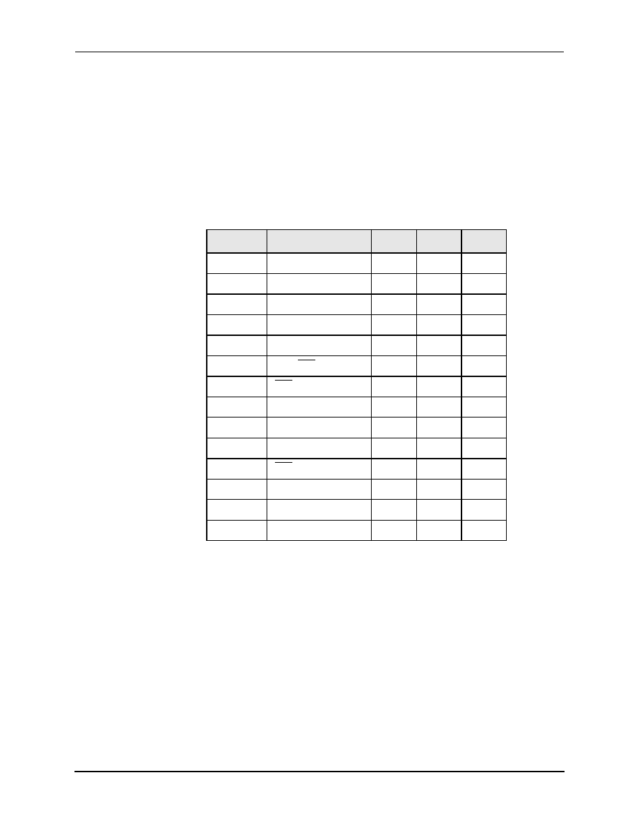
7.0 Electrical/Mechanical Specifications
RC224ATL/224ATLV
7.3 Interface Timing and Waveforms
EmbeddedModem Family
7-2
Conexant
D224ATLVDSC
7.3 Interface Timing and Waveforms
Table 7-2
lists the host bus interface timing parameters.
Figure 7-1
illustrates the
interface waveforms.
Table 7-3
lists the current and power requirements, and
Table 7-4
lists absolute maximum ratings.
Table 7-2. Timing≠Host Bus Interface
Symbol
Parameter
Min
Max
Units
t
AS
Address Setup
25
--
ns
t
AH
Address Hold
0
--
ns
t
CS
Chip Select Setup
10
--
ns
t
CH
Chip Select Hold
0
--
ns
t
RD
Read Strobe Width
100
--
ns
t
DD
Delay HRD to Data
--
75
ns
t
DRH
HRD to Data Hold
10
--
ns
t
WT
Write Strobe Width
75
--
ns
t
DS
Write Data Setup
30
--
ns
t
DWH
Write Data Hold
10
--
ns
t
DF
HRD to Driver Off
--
30
ns
t
DIS
HDIS Enable
--
40
ns
t
DIH
HDIS Hold
40
--
ns
t
INH
Interrupt Hold
--
100
ns
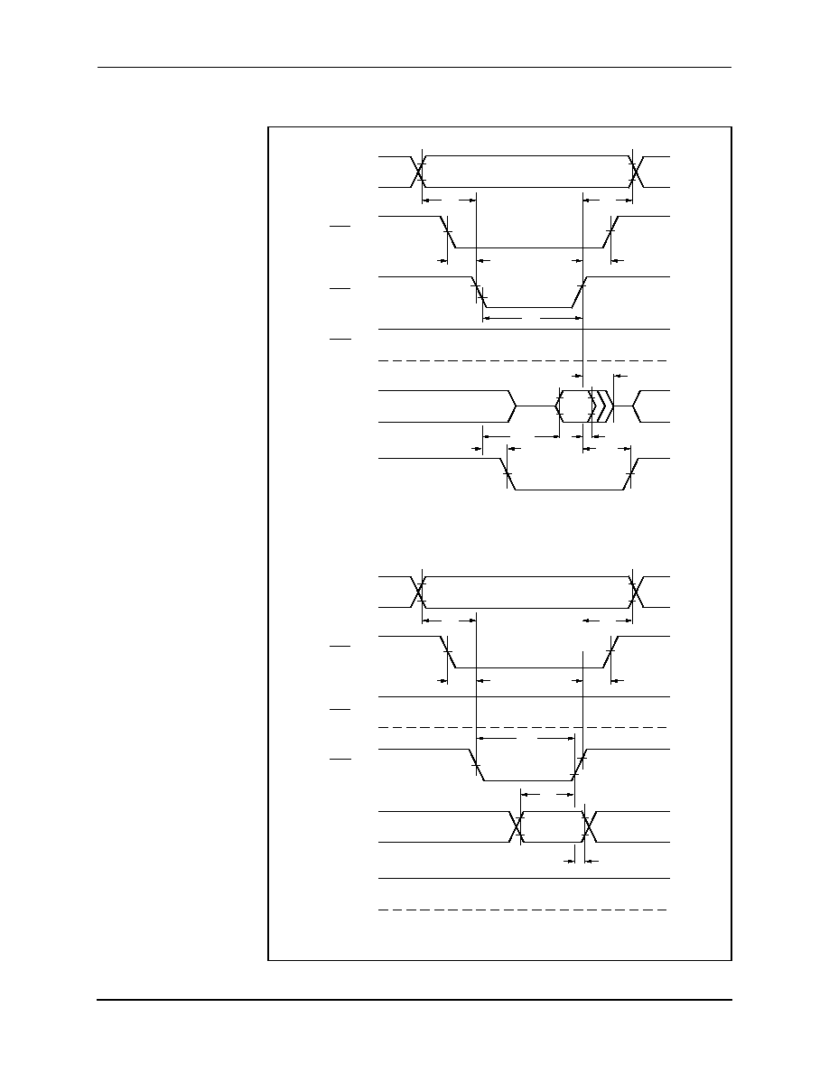
RC224ATL/224ATLV
7.0 Electrical/Mechanical Specifications
EmbeddedModem Family
7.3 Interface Timing and Waveforms
D224ATLVDSC
Conexant
7-3
Figure 7-1. Timing Waveform
tDD
tDIH
tDIS
tRD
tDF
tDRH
tAS
tCS
tCH
tAH
HA0-HA2
HCS
HRD
HWT
HD0-HD7
HDIS
a. Host Read
tDS
tWT
tDWH
tAS
tCS
tCH
tAH
HA0-HA2
HCS
HRD
HWT
HD0-HD7
HDIS
b. Host Write
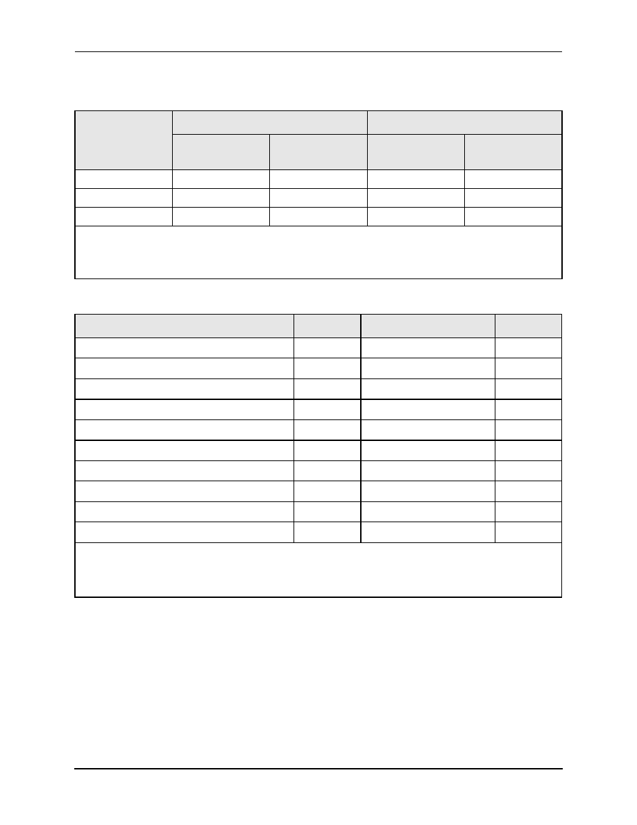
7.0 Electrical/Mechanical Specifications
RC224ATL/224ATLV
7.3 Interface Timing and Waveforms
EmbeddedModem Family
7-4
Conexant
D224ATLVDSC
Table 7-3. Current and Power Requirements
Mode
Current (ID)
Power (PD)
Typical
Current @ 25∞C
Maximum Current
@ 0∞C
Typical
Power @ 25∞C
Maximum
Power @ 0∞C
Operating
20 mA
22 mA
100 mW
110 mW
Sleep - Idle
5 mA
6 mA
25 mW
30 mW
Sleep - Stop
1 mA
1 mA
5 mW
5 mW
NOTE(S):
1. Test conditions: VDD = 5.0 V
DC
for typical values; VDD = 5.25 V
DC
for maximum values.
2. Test conditions: VDD = 3.3 V
DC
for typical values; VDD = 3.6 V
DC
for maximum values.
Table 7-4. Absolute Maximum Ratings
Parameter
Symbol
Limits
Units
Supply Voltage
V
DD
≠ 0.5 to + 7.0
V
Input Voltage
V
IN
≠ 0.5 to VCC + 0.5
V
Analog Inputs
V
IN
≠ 0.3 to + 5 VAA + 0.3
V
Voltage Applied to Outputs in High Z State
V
HZ
≠ 0.5 to + 5 VDD + 0.5
V
DC Input Clamp Current
I
IK
20
mA
DC Output Clamp Current
I
OK
20
mA
Static Discharge Voltage (@ 25∞C)
V
ESD
3000
V
Latch-Up Current (@ 25∞C)
I
TRIG
200
mA
Operating Temperature Range
T
A
≠ 0 to + 70
C
Storage Temperature Range
T
STG
≠ 40 to + 80
C
NOTE(S):
Stresses above those listed may cause permanent damage to the device. This is a stress rating only, and functional
operation at these or any other conditions above those listed in the operational section of this specification is not implied.
Exposure to absolute maximum rating conditions for extended periods may affect device reliability.

RC224ATL/224ATLV
7.0 Electrical/Mechanical Specifications
EmbeddedModem Family
7.3 Interface Timing and Waveforms
D224ATLVDSC
Conexant
7-5
Table 7-5
lists digital interface characteristics, and
Table 7-6
lists analog interface
characteristics.
Table 7-5. Digital Interface Characteristics
Parameter
Symbol
Min.
Typ.
Max
Units
Test Conditions
(1)
Input High Voltage
Type IA
Type DIO
Type IH
V
IH
2.0
2.4
≠ 30
--
--
--
V
CC
V
CC
30
V
DC
--
Input Low Voltage
Type IA, IC, and DO
V
IL
≠ 0.3
--
0.8
V
DC
--
Input Low Voltage
Type IF
V
IL
38
--
--
V
RMS
(2)
Input Leakage Current
IA and IC
I
IN
--
--
10
µAdc
V
IN
= 0 to V
CC
Output High Voltage
Type OA
Type OD
Type OG
Type OH
V
OH
2.4
--
--
5
--
--
--
8
--
V
CC
V
CC
--
V
DC
I
LOAD
= -100 µA
I
LOAD
= 0 mA
Output Low Voltage
Type OA
Type OB
Type OD
Type OG
Type OH
V
OL
--
--
--
0.5
≠ 8
--
--
0.75
--
≠ 5
0.4
0.4
--
--
--
V
DC
I
LOAD
= 1.6 mA
I
LOAD
= 0.8 mA
I
LOAD
= 15 mA
I
LOAD
= 8 mA
Three-State (off) Current
I
TS
--
--
25
µAdc
V
IN
= 0.8 V to 4.5 V
NOTE(S):
(1)
RC224ATL Test Conditions: V
CC
= 5 V 5%
,
T
A
= 0∞C to 70∞C (unless otherwise stated).
RC224ATLV Test Conditions: V
CC
= 3.3 V 5%
,
T
A
= 0∞C to 70∞C (unless otherwise stated).
Output loads: 50 pF + one TTL.
(2)
AC V
RMS
voltage between Tip and Ring, using the on-board modular DAA.

7.0 Electrical/Mechanical Specifications
RC224ATL/224ATLV
7.3 Interface Timing and Waveforms
EmbeddedModem Family
7-6
Conexant
D224ATLVDSC
Figure 7-2
shows the mechanical drawing of the 68-pin PLCC.
Table 7-7
lists its
dimensions.
Figure 7-3
shows the mechanical drawing of the 100-pin PQFP.
Table 7-8
lists
its dimensions.
Table 7-6. Analog Interface Characteristics
Name
Type
Characteristic
Value
RXA
I (DA)
Input impedance
>50 k
--
--
Voltage range
2.5 ± 1.6 V
TXA1, TXA2
O (DD)
Minimum load
300
--
--
Maximum capacitive load
0.01 µF
--
--
Output impedance
10
--
--
Output voltage
2.5 ± 1.6 V
--
--
DC offset
<200 mV
(1)
SPKR
O (DF)
Minimum load
300
--
--
Maximum capacitive load
0.01 µF
--
--
Output impedance
10
--
--
Output voltage
2.5 ± 1.6 V
--
--
DC offset
<20 mV
(1)
NOTE(S):
(1)
With Reference to VC (2.5 V nominal).
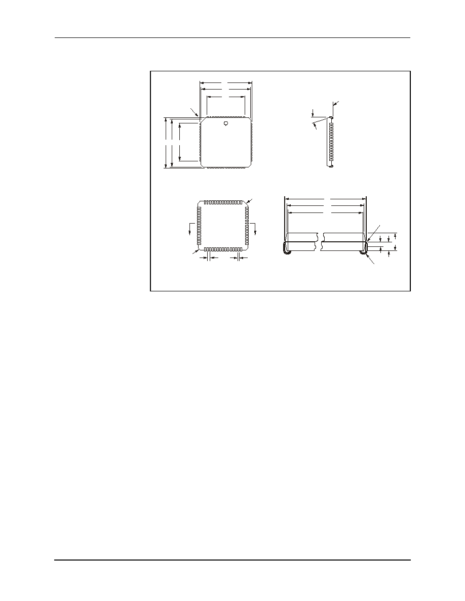
RC224ATL/224ATLV
7.0 Electrical/Mechanical Specifications
EmbeddedModem Family
7.3 Interface Timing and Waveforms
D224ATLVDSC
Conexant
7-7
Figure 7-2. 68-Pin PLCC
D D1 D2
D
D1
D2
D
D1
D3
INDEX
CORNER
TOP VIEW
TOP VIEW
BOTTOM VIEW
TYP. FOR EACH AXIS
(EXCEPT FOR BEVELED EDGE)
SECTION A-A
A
A
b
e
CHAM.
h x 45 DEG.
3 PLCS
CHAM.
J x 45 DEG.
SEATING
PLANE
R1
R
A
A1
A2

7.0 Electrical/Mechanical Specifications
RC224ATL/224ATLV
7.3 Interface Timing and Waveforms
EmbeddedModem Family
7-8
Conexant
D224ATLVDSC
Table 7-7. 68-Pin PLCC Dimensions
Dim
Millimeters
Inches
Min
Max
Min
Max
A
4.14
4.39
0.163
0.173
A1
1.37
1.47
0.054
0.058
A2
2.31
2.46
0.091
0.097
b
0.457 TYP
0.018 TYP
D
25.02
25.27
0.985
0.995
D1
24.00
24.26
0.945
0.955
D2
20.19
20.45
0.795
0.805
D3
23.24
23.5
0.915
0.925
e
1.27 BSC
0.050 BSC
h
0.254 TYP
0.010 TYP
J
1.15 TYP
0.045 TYP
45∞ TYP
45∞ TYP
R
0.89 TYP
0.035 TYP
R1
0.254 TYP
0.010 TYP
NOTE(S):
Reference: PD68J/GP00-D164
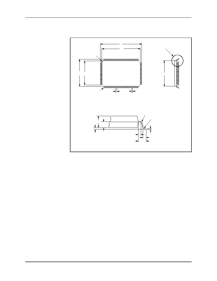
RC224ATL/224ATLV
7.0 Electrical/Mechanical Specifications
EmbeddedModem Family
7.3 Interface Timing and Waveforms
D224ATLVDSC
Conexant
7-9
Figure 7-3. 100-Pin PQFP
D
D1
E1
D
D1
TOP VIEW
SIDE VIEW
DETAIL A
b
a
PIN 1
REF
See
Detail A
CHAM.
H x 45 DEG.
(4x)
R1
R2
A
A1
K1
A2
K2
K3
J

7.0 Electrical/Mechanical Specifications
RC224ATL/224ATLV
7.3 Interface Timing and Waveforms
EmbeddedModem Family
7-10
Conexant
D224ATLVDSC
Table 7-8. 100-Pin PQFP Dimensions
Dim
Millimeters
Inches
Min
Max
Min
Max
A
1.95
2.05
0.077
0.081
A1
0.95
1.05
0.037
0.041
A2
0.15
0.25
0.006
0.010
D
22.96
23.44
0.904
0.923
D1
19.89
20.09
0.783
0.791
E
16.94
17.45
0.667
0.687
E1
13.89
14.10
0.547
0.555
K1
0.70
0.90
0.028
0.035
K2
0.40
--
0.016
--
K3
1.60 REF
0.083 REF
R1
0.13
--
0.005
--
R2
0.15
0.25
0.008
0.010
a
0.60
0.70
0.024
0.028
b
0.26
0.36
0.010
0.014
H
--
0.25
--
0.010
J
0.13
0.17
0.005
0.007
NOTE(S):
Reference: GP00-D234

D224ATLVDSC
Conexant
A-1
A
Appendix A: RC224ATF Modem Designs
This appendix describes two modem design examples. The schematics and parts
lists are provided for designs incorporating the RC224ATF packaged in a 68-pin
PLCC and implemented with either a parallel or serial interface.
A.1 68-Pin PLCC Design for Serial Interface
Figure A-1
and
Figure A-2
provide the schematic of a RC224ATF 68-pin PLCC
serial interface board design.
Table A-1
lists the bill of materials for this design.
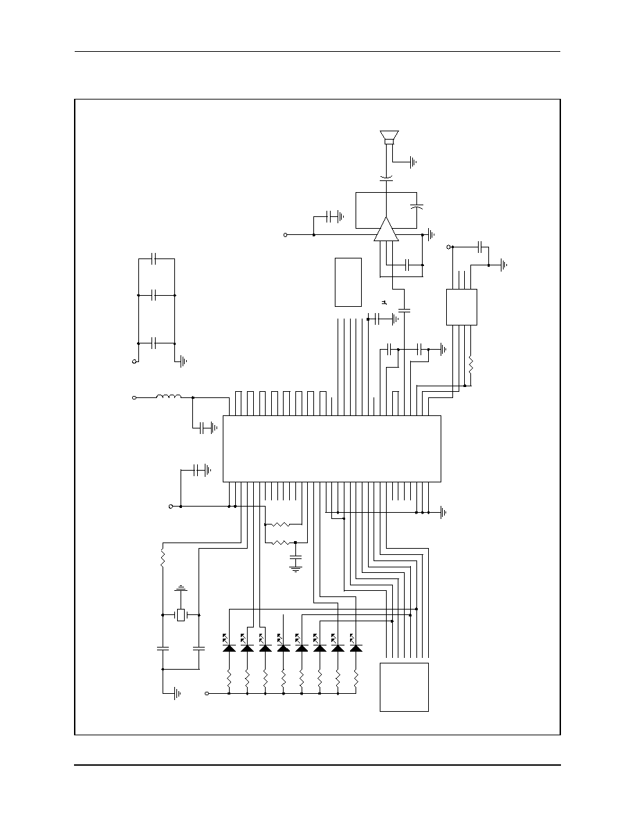
Appendix A: RC224ATF Modem Designs
RC224ATL/224ATLV
A.1 68-Pin PLCC Design for Serial Interface
EmbeddedModem Family
A-2
Conexant
D224ATLVDSC
Figure A-1. Serial Interface Design
DECOUPLING CA
P
S
TO V.24
EIA-232-
C
INTERFAC
E
TRANSCEIVE
R
S
TO DAA
INTERFACE
OH*
TXA2
TXA1
RXA
DTR*
RI*
CTS*
DSR*
RXD*
CI*
DCD*
TXD*
RING*
VCC
VCC
VCC
VCC
VCC
VCC
C5
2200
pF
R4
2.2K
C10
.1
C11 .1
C13
10
16V
LS1
16120
1
L1
47
C18
1000 p
F
C19
.1
F
C6 22 10V
C7
56 pF
5%
C17
56 pF
5%
Y1
1
6
.000312MHZ
1
2
3
C14
.1
+
-
U6
LM386
2
3
5
6
1
4
8
7
U2
HY93C46J
3
5
2
8
4
6
7
1
CS
DI
VCC
NC
SK
DO
GND
NC
C16
220
16V
C15
.1
C12
.1
C22 .1
C9 12
10%
20V
C21
.1
R17
4.7K
U7
R6781-11
15
66
59
58
10
1
56
30
46
44
41
37
57
14
11
67
2
20
21
6
19
68
63
13
65
64
62
4
12
17
18
5
60
61
53
29
49
28
52
27
50
26
47
25
45
24
51
48
23
22
43
38
40
33
32
31
36
3
9
35
34
55
42
54
39
8
16
7
VCC
NMI*
XTLO
XTLI
AAE*
DCDL*
PH2
NC
NC
NC
NC
NC
TEST*
RESET*
DTRL*
MR*
IDLENO
DTR*
IDLEN1
WAKEUP*
TXD*
RI*
CTS*
RXD*
CI*/HS
DCD*
DSR*
NC
NC
NC
NC
SEREN*
DGND1
DGND2
VAA
TDACO
TDACI
MODEO
MODEI
TRSTO
TRSTI
RRSTO
RRSTI
RSTBO
RSTBI
TSTBO
TSTBI
RADCO
RADCI
RAGCO
RAGCI
TLKRLY*
OHRLY*
RXA
TXA1
TXA2
VC
RING*
A/A1*
AGCIN
RFILO
SLEEP*
SLEEPI*
SPKR
AGND
NVRDIO
NVRSK
NVRCS
R13
2K
D6
R14
2K
D7
R15
2K
D8
R18
2
K
D9
R19
2K
D10
R20
2K
D11
R21
2K
D12
R22
2K
D13
R16
330K
C8
.1
R12
100
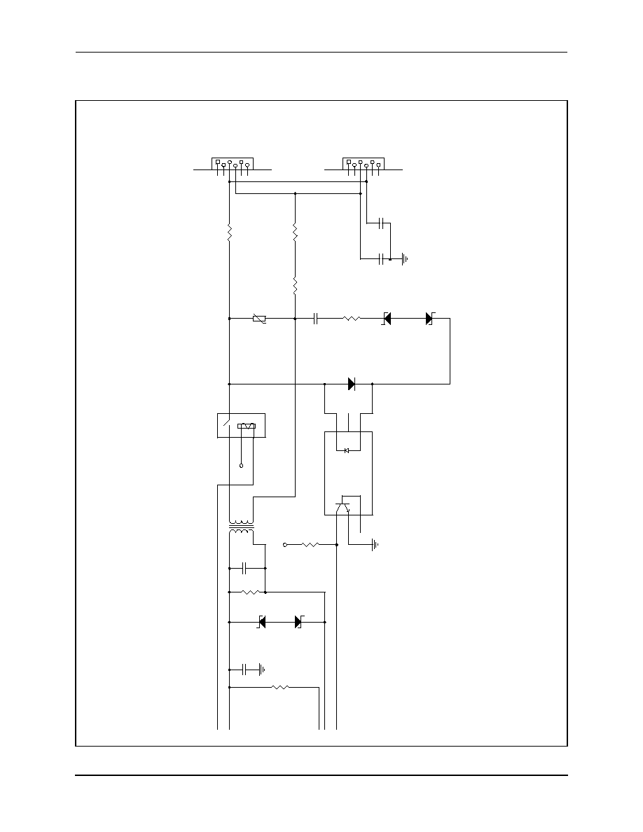
RC224ATL/224ATLV
Appendix A: RC224ATF Modem Designs
EmbeddedModem Family
A.1 68-Pin PLCC Design for Serial Interface
D224ATLVDSC
Conexant
A-3
Figure A-2. Serial Interface Design DAA
OH*
TXA1
TXA2
RING*
RXA
VCC
VCC
R1
18
1W
RV1
V150LA
2
TOP
J4
T
E
L
CO4/6
1
2
3
4
5
6
8
7
R2
7.5K
1W
D1
1
N
970B
D2
1
N
970B
LINE
T1
TTC14
3
K1
RELAY
1
4
2
3
C4 .01
D5
1
N
749A
R3
100K
R6
536 1%
R9
1.5K
D4
1
N
749A
C20 .1
U1
4N3
5
6
4
5
1
3
2
D3
1
N
4148
R11
0
R10
0
C2 .001 10%
1KV
C3 .47 10% 250V
C1
.001
10% 1KV
TOP
J3
T
E
L
CO4/6
1
2
3
4
5
6
8
7

Appendix A: RC224ATF Modem Designs
RC224ATL/224ATLV
A.1 68-Pin PLCC Design for Serial Interface
EmbeddedModem Family
A-4
Conexant
D224ATLVDSC
Table A-1. Serial Bill of Materials (1 of 2)
Item
Quantity
Reference
Part
1
2
C2,C1
0.001
2
1
C3
0.47
3
1
C4
.01
4
1
C5
2200 pF
5
1
C6
22
6
2
C7,C17
56 pF
7
9
C8,C10,C11,C12,C14,C15,C19,
C20,C21
0.1
8
1
C9
12
9
1
C13
10
10
1
C16
220
11
1
C18
1000 pF
12
2
D1,D2
1N970B
13
1
D3
1N4148
14
2
D5,D4
1N749A
15
8
D6,D7,D8,D9,D10,D11,D12,D13
16
2
J4,J3
TELCO4/6
17
1
K1
RELAY
18
1
LS1
161201
19
1
L1
47
20
1
RV1
V150LA2
21
1
R1
18
22
1
R2
7.5 k
23
1
R3
100 k
24
1
R4
2.2 k
25
1
R6
536
26
1
R9
1.5 k
27
2
R11,R10
0
28
1
R12
100
29
8
R13,R14,R15,R18,R19,R20,R21,
R22
2 k
RC224ATL/224ATLV
Appendix A: RC224ATF Modem Designs
EmbeddedModem Family
A.1 68-Pin PLCC Design for Serial Interface
D224ATLVDSC
Conexant
A-5
30
1
R16
330 k
31
1
R17
4.7 k
32
1
T1
TTC143
33
1
U1
4N35
34
1
U2
HY93C46J
35
1
U6
LM386
36
1
U7
R6781-11
37
1
Y1
16.000312 MHz
Table A-1. Serial Bill of Materials (2 of 2)
Item
Quantity
Reference
Part

Appendix A: RC224ATF Modem Designs
RC224ATL/224ATLV
A.2 68-Pin PLCC Design for Parallel Interface
EmbeddedModem Family
A-6
Conexant
D224ATLVDSC
A.2 68-Pin PLCC Design for Parallel Interface
Figure A-3
and
Figure A-4
provide the schematic of a RC224ATF 68-pin PLCC
parallel interface board design.
Table A-2
lists the bill of materials for this design.
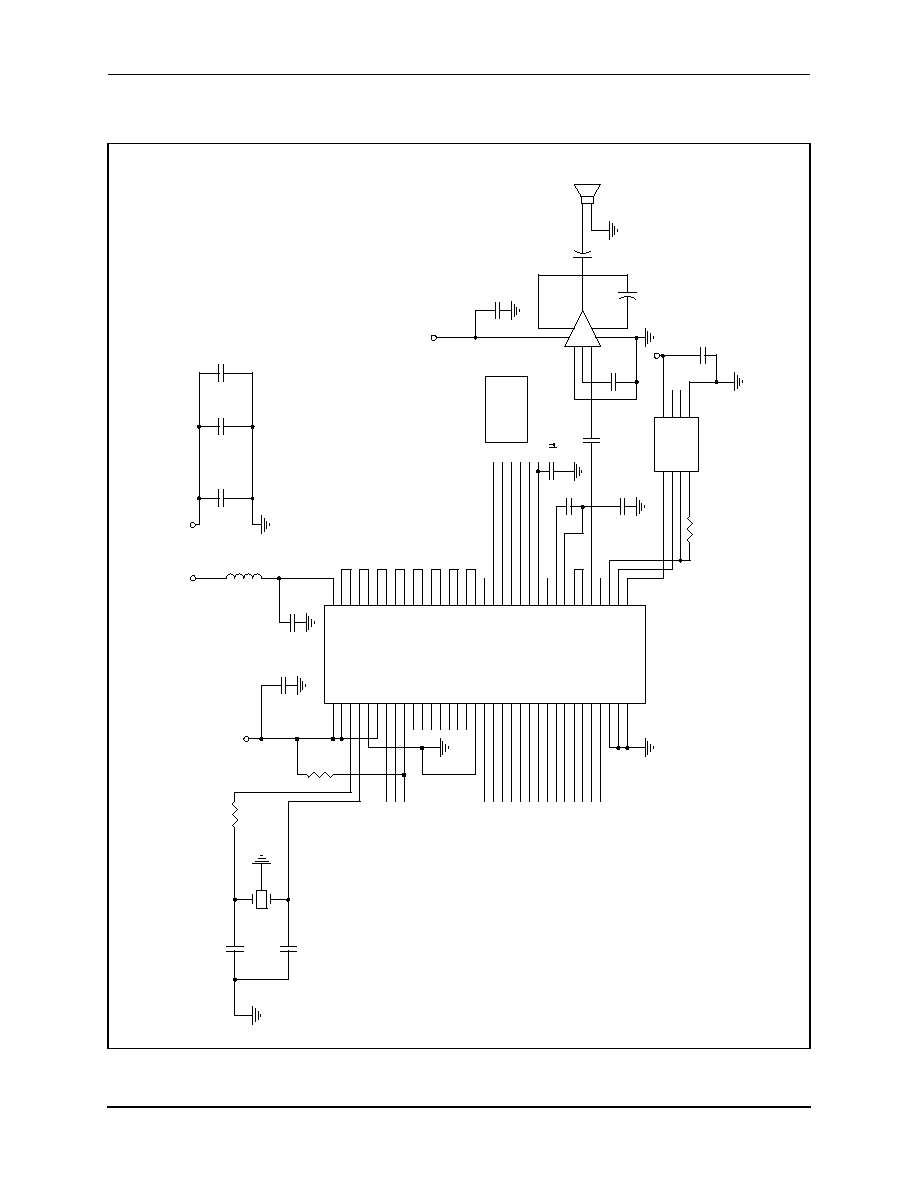
RC224ATL/224ATLV
Appendix A: RC224ATF Modem Designs
EmbeddedModem Family
A.2 68-Pin PLCC Design for Parallel Interface
D224ATLVDSC
Conexant
A-7
Figure A-3. Parallel Interface Design
DECOUPLING CA
P
S
TO DAA
INTERFAC
E
HCS*
HDIS
OH*
TXA2
RING*
HWT*
HRD*
HA0
HA1
HA2
RESE
T
*
HINT
HD0
HD1
HD2
HD3
HD4
HD5
HD6
HD7
TXA1
RXA
VCC
VCC
VCC
VCC
VCC
C5 2200
pF
R4
2.2K
C10
.1
C11
.1
C13
10
16V
L1 47
C6
22 10V
C
56P
F
5%
C1
56P
5%
C14
.1
+
-
U6
LM386
2
3
5
6
1
4
8
7
U2
HY93C46J
3
5
2
8
4
6
7
1
CS
DI
VCC
NC
SK
DO
GND
NC
C15
.1
C8
.1
C9 12 10%
20V
C21
.1
R13
10K
U7
R
6
781
15
66
59
58
12
57
16
6
17
37
41
44
46
30
18
20
21
62
63
64
65
67
68
1
2
5
4
11
10
8
14
60
61
39
53
29
49
28
52
27
50
26
47
25
45
24
51
48
23
22
43
38
40
33
32
31
36
3
9
35
34
55
42
54
56
19
13
7
VCC
NMI*
XTLO
XTLI
IDLENO
TEST*
HINT
HCS*
HDIS
NC
NC
NC
NC
NC
NC
NC
IDLENI
HD0
HD1
HD2
HD3
HD4
HD5
HD6
HD7
HWT*
HRD*
HA0
HA1
HA2
RESET*
DGND1
DGND2
AGND
VAA
TDACO
TDACI
MODEO
MODEI
TRSTO
TRSTI
RRSTO
RRSTI
RSTBO
RSTBI
TSTBO
TSTBI
RADCO
RADCI
RAGCO
RAGCI
TLKRLY*
OHRLY*
RXA
TXA1
TXA2
VC
RING*
A/A1*
AGCIN
RFILO
SLEEP*
SLEEPI*
SPKR
PH2
NVRDIO
NVRSK
NVRCS
C19 .1
F
R12
100
C16 220
16V
C18 1000 p
F
C12
.1
Y1
1
6
.000312MHZ
1
2
3
LS1
16120
1
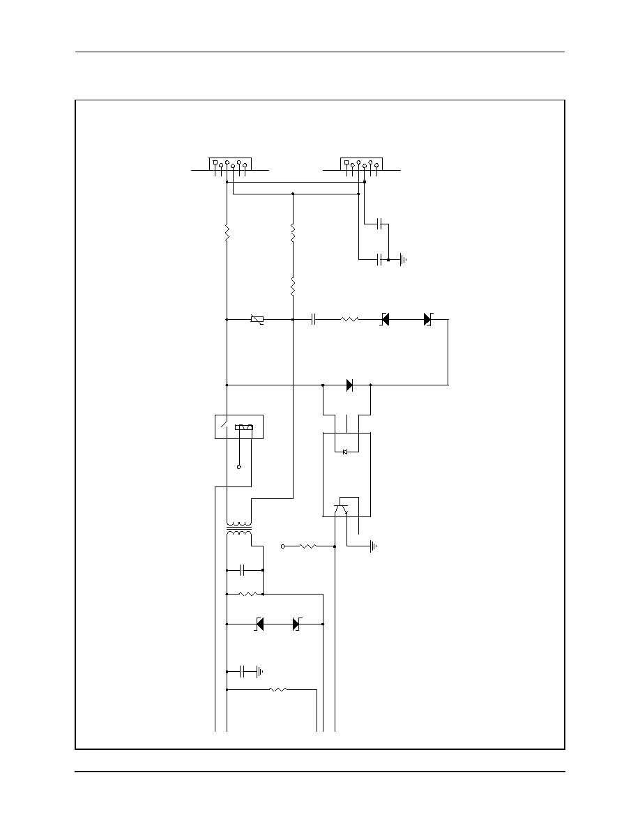
Appendix A: RC224ATF Modem Designs
RC224ATL/224ATLV
A.2 68-Pin PLCC Design for Parallel Interface
EmbeddedModem Family
A-8
Conexant
D224ATLVDSC
Figure A-4. Parallel Interface Design DAA
OH*
TXA1
TXA2
RING*
RXA
VCC
VCC
R1
18 1W
RV1
V150LA
2
TOP
J4
T
E
L
CO4/6
1
2
3
4
5
6
8
7
R2
7.5K
1W
D1
1
N
970B
D2
1
N
970B
LINE
T1
TTC14
3
K1
RELAY
1
4
2
3
C4 .01
D5
1
N
749A
R3
100K
R6
536
1%
R9
1.5K
D4
1
N
749A
C20 .1
U1
4N3
5
6
4
5
1
3
2
D3
1
N
4148
R11
0
R10
0
C2 .001 10% 1KV
C3
.47 10% 250V
C1 .001 10% 1KV
TOP
J3
T
E
L
CO4/6
1
2
3
4
5
6
8
7

RC224ATL/224ATLV
Appendix A: RC224ATF Modem Designs
EmbeddedModem Family
A.2 68-Pin PLCC Design for Parallel Interface
D224ATLVDSC
Conexant
A-9
Table A-2. Parallel Billing Materials (1 of 2)
Item
Quantity
Reference
Part
1
2
C2,C1
0.001
2
1
C3
0.47
3
1
C4
0.01
4
1
C5
2200 pF
5
1
C6
22
6
2
C7,C17
56 pF
7
8
C8,C10,C11,C12,C14,C15,C20,
C21
0.1
8
1
C9
12
9
1
C13
10
10
1
C16
220
11
1
C18
1000 pF
12
1
C19
0.1 µF
13
2
D1,D2
1N970B
14
1
D3
1N4148
15
2
D5,D4
1N749A
16
2
J4,J3
TELCO4/6
17
1
K1
RELAY
18
1
LS1
161201
19
1
L1
47
20
1
RV1
V150LA2
21
1
R1
18
22
1
R2
7.5 k
23
1
R3
100 k
24
1
R4
2.2 k
25
1
R6
536
26
1
R9
1.5 k
27
2
R11,R10
0
28
1
R12
100
29
1
R13
10 k
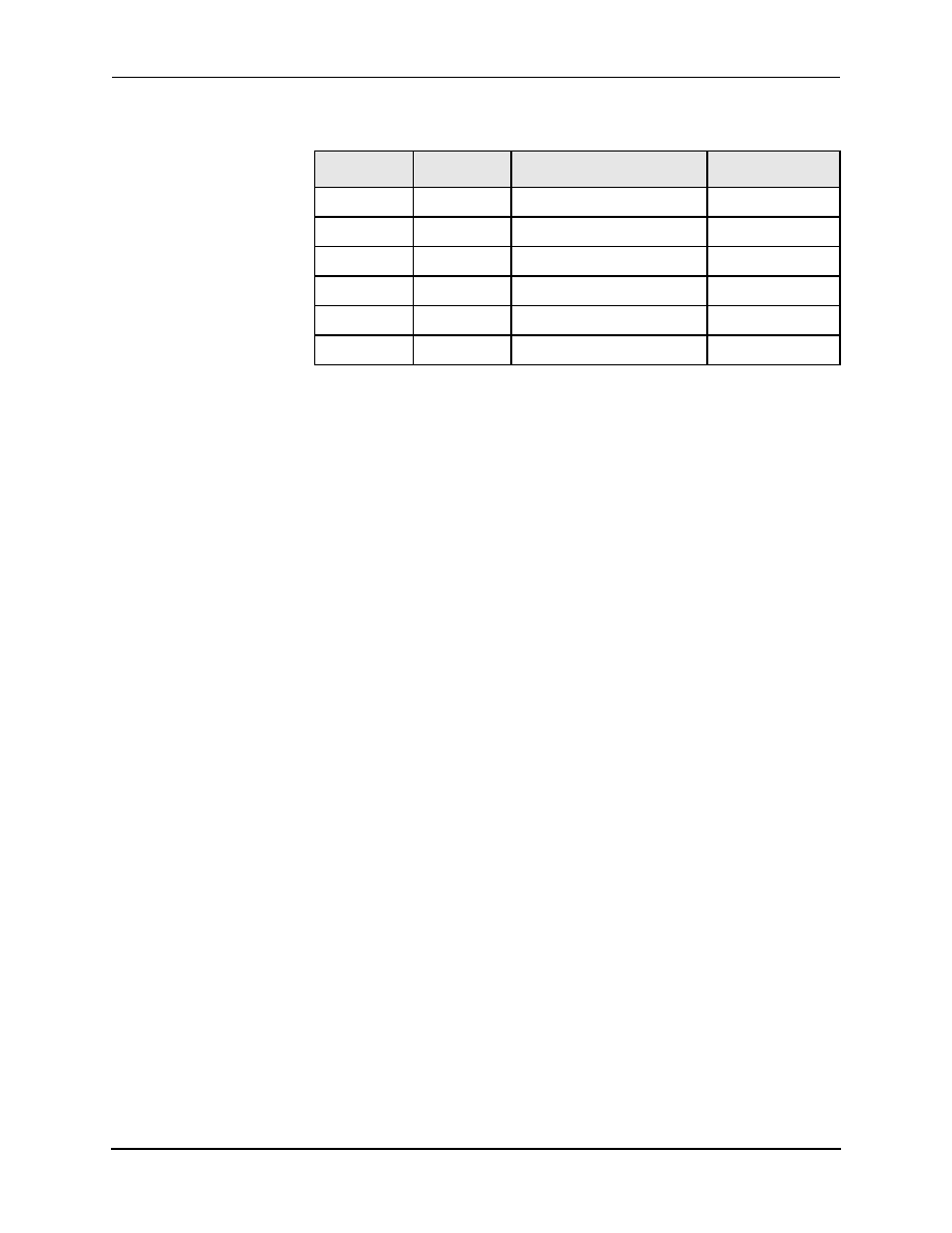
Appendix A: RC224ATF Modem Designs
RC224ATL/224ATLV
A.2 68-Pin PLCC Design for Parallel Interface
EmbeddedModem Family
A-10
Conexant
D224ATLVDSC
30
1
T1
TTC143
31
1
U1
4N35
32
1
U2
HY93C46J
33
1
U6
LM386
34
1
U7
R6781
35
1
Y1
16.000312 MHz
Table A-2. Parallel Billing Materials (2 of 2)
Item
Quantity
Reference
Part

D224ATLVDSC
Conexant
B-1
B
Appendix B: Acronyms/Abbreviations
A-B
AGC
Automatic Gain Control
AT
Attention Code
C
CCITT
International Telegraph and Telephone Consultative
Committee
CRC
Cyclic Redundancy Check
CTS
Clear to Send
D
DAC
Digital-to-Analog Converter
DCE
Data Communication Equipment
DTE
Host Data Terminal Equipment
DTMF
Dual-Tone Multifrequency
DTR
Data Terminal Ready (name of bit and function)
E-F
EOP
End of Process
FCS
Frame Check Sequence
I
IER
Interrupt Enable Register
IIR
Interrupt Identifier Register
L
LCR
Line Control Register
LED
Light Emitting Diode
LSR
Line Status Register

Appendix B : Acronyms/Abbreviations
RC224ATL/224ATLV
EmbeddedModem Family
B-2
Conexant
D224ATLVDSC
M
MCR
Modem Control Register
MCU
Microcontroller Unit
MSR
Modem Status Register
O-P
OEM
Original Equipment Manufacturer
op amp
operational amplifier
PBX
Private Branch Exchange
R-S
RBR
Receiver Buffer Register
RTS
Request to Send (name of bit and function)
SCR
Scratchpad Register
T-U
THR
Transmit Holding Register
TTL
Transistor-to-Transistor Logic
UART
Universal Asynchronous Receiver/Transmitter
X
X-on/X-off
Transistor On/Off


Further Information
literature@conexant.com
1-800-854-8099 (North
America)
33-14-906-3980
(International)
Web Site
www.conexant.com
World Headquarters
Conexant Systems, Inc.
4311 Jamboree Road
P. O. Box C
Newport Beach, CA
92658-8902
Phone: (949) 483-4600
Fax: (949) 483-6375
U.S. Florida/South America
Phone: (813) 799-8406
Fax: (813) 799-8306
U.S. Los Angeles
Phone: (805) 376-0559
Fax: (805) 376-8180
U.S. Mid-Atlantic
Phone: (215) 244-6784
Fax: (215) 244-9292
U.S. North Central
Phone: (630) 773-3454
Fax: (630) 773-3907
U.S. Northeast
Phone: (978) 692-7660
Fax: (978) 692-8185
U.S. Northwest/Pacific West
Phone: (408) 249-9696
Fax: (408) 249-7113
U.S. South Central
Phone: (972) 733-0723
Fax: (972) 407-0639
U.S. Southeast
Phone: (770) 246-8283
Fax: (770) 246-0018
U.S. Southwest
Phone: (949) 483-9119
Fax: (949) 483-9090
APAC Headquarters
Conexant Systems
Singapore,
Pte. Ltd.
1 Kim Seng Promenade
Great World City
#09-01 East Tower
Singapore 237994
Phone: (65) 737 7355
Fax: (65) 737 9077
Australia
Phone: (61 2) 9869 4088
Fax: (61 2) 9869 4077
China
Phone: (86 2) 6361 2515
Fax: (86 2) 6361 2516
Hong Kong
Phone: (852) 2827 0181
Fax: (852) 2827 6488
India
Phone: (91 11) 692 4780
Fax: (91 11) 692 4712
Korea
Phone: (82 2) 565 2880
Fax: (82 2) 565 1440
Europe Headquarters
Conexant Systems France
Les Taissounieres B1
1681 Route des Dolines
BP 283
06905 Sophia Antipolis
Cedex
France
Phone: (33 4) 93 00 33 35
Fax: (33 4) 93 00 33 03
Europe Central
Phone: (49 89) 829 1320
Fax: (49 89) 834 2734
Europe Mediterranean
Phone: (39 02) 9317 9911
Fax: (39 02) 9317 9913
Europe North
Phone: (44 1344) 486 444
Fax: (44 1344) 486 555
Europe South
Phone: (33 1) 41 44 36 50
Fax: (33 1) 41 44 36 90
Middle East Headquarters
Conexant Systems
Commercial (Israel) Ltd.
P. O. Box 12660
Herzlia 46733, Israel
Phone: (972 9) 952 4064
Fax: (972 9) 951 3924
Japan Headquarters
Conexant Systems Japan
Co., Ltd.
Shimomoto Building
1-46-3 Hatsudai,
Shibuya-ku, Tokyo
151-0061 Japan
Phone: (81 3) 5371-1567
Fax: (81 3) 5371-1501
Taiwan Headquarters
Conexant Systems, Taiwan
Co., Ltd.
Room 2808, 333
International Trade Building
Keelung Road, Section 1
Taipei 110, Taiwan, ROC
Phone: (886 2) 2720 0282
Fax: (886 2) 2757 6760
cross ref
0.0 Sales Offices