 | –≠–ª–µ–∫—Ç—Ä–æ–Ω–Ω—ã–π –∫–æ–º–ø–æ–Ω–µ–Ω—Ç: RC56D-USB | –°–∫–∞—á–∞—Ç—å:  PDF PDF  ZIP ZIP |

'DWD 6KHHW
2UGHU 1R 0'
5HY 'HFHPEHU
5&'86%
,QWHJUDWHG9.IOH[
0RGHP'HYLFH6HWVZLWK86%,QWHUIDFHIRU'HVNWRS$SSOLFDWLRQV
Introduction
The CONEXANT
TM
RC56D Modem Device Set supports
the USB (Universal Serial Bus), as described by the
Universal Serial Bus Specification Revision 1.0. USB
provides a flexible interconnect between a PC and a wide
range of peripherals, such as to a CONEXANT modem
device set.
The CONEXANT RC56D family devices, in conjunction
with the R8292 USB controller provide a complete USB
modem solution. The supported modem feature set for the
USB modem solution is the same as the standard RC56D
parallel host interface device set (see "RC56D and
RC336D Integrated V.90/K56flex/V.34 Modem Device Set
for Desktop Applications" Data Sheet, Order No. MD211).
The modem models, which include the R8292 UCU (USB
Controller Unit in 68-PLCC), are listed in Table 1.
Hardware
A complete accelerator kit implementing the USB solution
is offered as "Perth" (AK56-D540). This design consists of
the RC56D parallel host interface device set and the
R8292 USB Controller Unit (UCU). The R8292 operates
with a 12 MHz crystal. A 32K x 8, 150 ns EEPROM is
required for USB controller firmware. Additionally, one
latch, one transistor, and two bus transceivers are
required.
The R8292 USB Controller is based on the MCS
Æ
51
microcontroller. It is a hubless USB peripheral controller
that supports suspend/resume modes and
isochronous/non-isochronous transfers.
Firmware
Firmware for the R8292 controller is provided in object
form, however, vendor specific descriptors can be
customized with a supplied utility. Vendor ID, Product ID,
Device Release Number, Manufacturer Name, Product
Name, and Serial Number can all be modified.
Drivers
A complete set of software drivers is provided for
Windows 98 and Windows 95 OSR 2.1 support. Sample
INF files are also provided.
Features
∑
All features supported by the RC56D family (see data
sheet Order No. MD211)
∑
Universal Serial Bus Specification Rev 1.0 compliant
∑
Three function endpoint pairs with corresponding
transmit/receive FIFO pairs
∑
Automatic transmit/receive FIFO management
∑
USB full speed 12Mbps
∑
USB low speed 1.5Mbps
∑
Reset separation
∑
Four LED driver outputs
∑
On-chip phase-locked loop (PLL)
∑
On-chip USB transceivers
∑
256 bytes on-chip Data RAM
∑
Suspend/Resume
∑
Vendor specific descriptors
∑
Windows 98 support
∑
Windows 95 OSR 2.1 support
∑
Extension pickup/remote hang-up detection
∑
Line-in-use detection
5&'86%
,QWHJUDWHG9.IOH[0RGHP'HYLFH6HWVZLWK86%,QWHUIDFH
0'
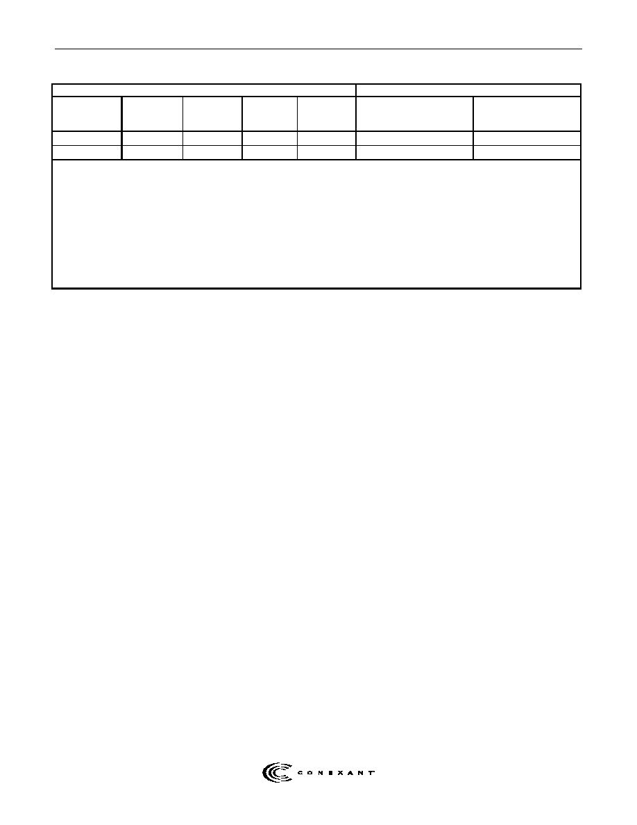
Table 1. Modem Models and Functions
0RGHO2UGHU3DUW 1XPEHUV
6XSSRUWHG )XQFWLRQV
0DUNHWLQJ
0RGHO 1XPEHU
'HYLFH 6HW
2UGHU 1XPEHU
0&8
>34)3@
3DUW 1R
0'3
>34)3@
3DUW 1R
8&8
>3/&&@
3DUW 1R
9 .IOH[ 'DWD 9 )D[
)D[ &O DQG 9RLFH7$0
+RVW '69' 9
)'63 $XGLR6SDQ
5&'6386%
'6/
/
5
5
<
<
5&'86%
'6/
/
5
5
<
±
1RWHV
0RGHO RSWLRQV
'
'RZQORDGDEOH
63
6SHDNHUSKRQH
86%
86% LQWHUIDFH
6XSSRUWHG IXQFWLRQV < 6XSSRUWHG ± 1RW VXSSRUWHG�
$XGLR6SDQ
$QDORJ VLPXOWDQHRXV YRLFH DQG GDWD
'69'
'LJLWDO VLPXOWDQHRXV YRLFH DQG GDWD
)D[ &O DQG
)D[ &ODVV DQG )D[ &ODVV VXSSRUW
)'63
)XOOGXSOH[ VSHDNHUSKRQH
9RLFH7$0
9RLFH DQG WHOHSKRQH DQVZHULQJ PDFKLQH VXSSRUW KDQGVHW VXSSRUW UHTXLUHV 63 PRGHO�
5 LV WKH &21(;$17 LQWHUQDO SDUW QXPEHU IRU WKH ,QWHO $$
Information provided by CONEXANT SYSTEMS, INC. is believed to be accurate and reliable. However, no responsibility is assumed by CONEXANT for its use, nor
any infringement of patents or other rights of third parties which may result from its use. No license is granted by implication or otherwise under any patent rights of
CONEXANT other than for circuitry embodied in CONEXANT products. CONEXANT reserves the right to change circuitry at any time without notice. This document
is subject to change without notice.
K56flex is a trademark of CONEXANT SYSTEMS, INC. and Lucent Technologies.
CONEXANT, "What's Next in Communications Technologies", MNP 10EC, and ConfigurACE are trademarks of CONEXANT SYSTEMS, INC.
MNP is a trademark of Compaq Computer Corporation.
MCS is a registered trademark of Intel Corporation.
©1998, CONEXANT SYSTEMS, INC.
Printed in U.S.A.
All Rights Reserved
,QWHJUDWHG9.IOH[0RGHP'HYLFH6HWVZLWK86%,QWHUIDFH
5&'86%
0'
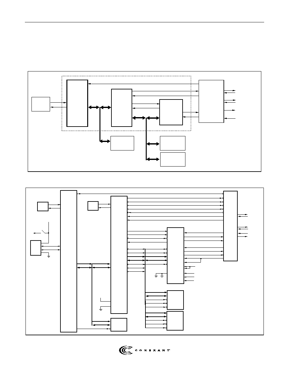
System Architecture
Hardware Interface
A system block diagram is shown in Figure 1.
The major interface signals are shown in Figure 2.
MD234F1 BD
TELEPHONE
LINE/
TELEPHONE
HANDSET/
AUDIO
INTERFACE
CIRCUIT
TELEPHONE
LINE
TEL HANDSET
MICROPHONE
HEADPHONE/
SPEAKER
MODEM DEVICE SET
MICRO
CONTROLLER
UNIT
(MCU)
[80-PIN PQFP]
(L2800)
MODEM
DATA PUMP
(MDP)
[100-PIN PQFP]
(R6764)
USB
CONTROLLER
UNIT
(UCU)
[68-PIN PLCC]
(R8292/
80931AA)
1M (128K x 8)
RAM
2M (256K x 8)
ROM/FLASH ROM
32K x 8
ROM
USB
INTERFACE
Figure 1. Block Diagram
MICRO
CONTROLLER
UNIT
(MCU)
MD234F2 IF
MODEM
DATA
PUMP
(MDP)
RS0-RS4
~CS
EXTERNAL
BUS
RIN
TXA1
TXA2
TELIN*
TELOUT*
SPKM
MICV*
MICM**
~RINGWAKE
~RLY1 (~OH)
~RLY2 (~VOICE)
~RLY3 (~MUTE)
~RLY4 (~CALLID)
~EXTOH
LCS
RINGD
VD3.3
CLKOUT
~WKRESOUT
DPIRQ
~READ
~WRITE
A0-A17
D0-D7
~DPSEL
~ROMSEL
~RAMSEL
~READ
~WRITE
A0-A4
D0-D7
~DPSEL
TELEPHONE
LINE
TELEPHONE
HANDSET
MICROPHONE
TELEPHONE
LINE/
TELEPHONE
HANDSET/
AUDIO
INTERFACE
CIRCUIT
HEADPHONE/
SPEAKER
~RES1
~RES2
2M (256K X 8)
ROM/
FLASH ROM
A0-A16
D0-D7
~READ
~WRITE
~RAMSEL
1M (128K X 8)
RAM
A0-A17
D0-D7
~READ
~WRITE
~ROMSEL
VGG
AVDD
VAA
DGND, AGND
SVCC (+5V)
SVCC (+5V)
SVCC (+5V)
VCC
~RESET
A0-A2
D0-D7
A0-A15
D0-D7
32K X 8
ROM
USB
CONTROLLER
UNIT
(UCU)
USB
A0-A15
D0-D7
~READ
D+
D-
VDD
SVCC (+5V)
DGND
CRYSTAL
CIRCUIT
XTAL1
XTAL2
SVCC
VDD
CLKIN
~WKRES
IRQ
CRYSTAL
CIRCUIT
XTLI
XTLO
* SP MODEL.
** NON-SP MODEL.
Figure 2. Hardware Interface Signals
5&'86%
,QWHJUDWHG9.IOH[0RGHP'HYLFH6HWVZLWK86%,QWHUIDFH
0'
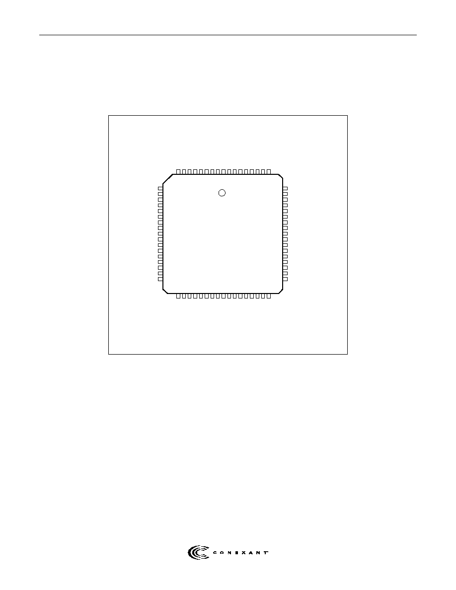
R8292 Signal Pin Assignments and Descriptions
The R8292 68-pin PLCC signal pin assignments are shown in Figure 3.
The R8292 68-pin PLCC signals are described in Table 2.
P0.7
P0.6
P0.5
P0.4
P0.3
P0.2
P0.1
P0.0
VSS
VCC
P3.0
P3.1/SOF#
P3.2/INT0#
P3.3/INT1#
P3.4
P3.5
WR#
Reserved (NC)
Reserved (NC)
Reserved (NC)
Reserved (NC)
VCC
DP0
DM0
ECAP
VSSP
VCCP
VSS
Reserved (NC)
Reserved (NC)
VSSP
Reserved (NC)
Reserved (NC)
LED0
P2.0
P2.1
P2.2
P2.3
P2.4
P2.5
P2.6
P2.7
VSS
VCCP
EA#
ALE
PSEN#
FSSEL
VSSP
Reserved (NC)
Reserved (NC)
RD#
P1.0/T2
P1.1/T2EX
P1.2
P1.3
P1.4
P1.5
P1.6
P1.7
LED3
LED2
XTAL1
XTAL2
AVCC
RST
PLLSEL
LED1
9
8
7
6
5
4
3
2
1
68
67
66
65
64
63
62
61
60
59
58
57
56
55
54
53
52
51
50
49
48
47
46
45
44
10
11
12
13
14
15
16
17
18
19
20
21
22
23
24
25
26
27
28
29
30
31
32
33
34
35
36
37
38
39
40
41
42
43
MD234F3 PO R8292 68PLCC
Figure 3. R8292 68-Pin PLCC Pin Signals

,QWHJUDWHG9.IOH[0RGHP'HYLFH6HWVZLWK86%,QWHUIDFH
5&'86%
0'
Table 2. R8292 68-Pin PLCC Pin Signal Descriptions
Signal Name
Type
Description
ALE
O
Address Latch Enable. ALE signals the start of an external bus cycle and indicates that valid address
information is available on lines A15:8 and AD7:0. An external latch can use ALE to demultiplex the address
from the address/data bus.
AVCC
PWR
Analog VCC. AVCC input for the phase locked loop circuitry.
DM0, DP0
I/O
USB Port 0. DP0 and DM0 are the differential data plus and data minus signals of USB port 0, the upstream
differential port. These lines do not have internal pullup resistors. Provide an external 1.5 K
pullup resistor
at DP0. If DP0 is not pulled high, a continuous SEO (USB reset) will be applied to these inputs causing the
8x931 to stay in reset.
EA#
I
External Access. Directs program memory accesses to on-chip or off-chip code memory. For EA# strapped
to ground, all program memory accesses are off-chip. For EA# strapped to VCC , program accesses on-chip
ROM if the address is within the range of the on-chip ROM; otherwise the access is off-chip. The value of
EA# is latched at reset. For devices without on-chip ROM, EA# must be strapped to ground.
ECAP
I
External Capacitor. Connect a 2.2 µF capacitor between this pin and VSS to ensure proper operation of the
differential line drivers.
FSSEL
I
Full Speed Select. Connect to VCC for 12MHz Xtal and 12Mbps full speed USB rate.
INT1#
I
HINT. Host bus interrupt input is set high by MCU when the MCU receiver error flag, received data available,
transmitter holding register empty, or modem status interrupt is asserted.
INT0#
I
RINGWAKE. Used to notify the host of an incoming ring in order to come out of suspend mode.
LED3:0
O
LED Drivers. Designed to drive LEDs connected directly to VCC. NC.
OVRI#/P3.0
I
Overcurrent Sense. Sense input to indicate an overcurrent condition on an external down-stream port.
Active low with an internal pullup. NC.
P0.7:0
I/O
Address/Data Lines. Eight-bit, open-drain, bidirectional I/O lines with Schmitt trigger inputs that represent
lower byte of external memory address multiplexed with data.
P1.7
I/O
NC. Quasi-bidirectional I/O port with internal pullup.
P1.6
O
Ready Indicate. Active low output to drive READY LED. Port has internal pullup.
P1.5
O
DCD Indicate. Active low output to drive DCD LED. Port has internal pullup.
P1.4
O
DATA Indicate. Active low output to drive DATA LED. Port has internal pullup.
P1.3
O
MODEMPWRCNTRL. Active low output used to control power supply to non-USB side of isolation. Port has
internal pullup.
P1.2
O
MDMRESET. Active low output used to reset the MCU and MDP. This port has an internal pullup.
P1.1
I/O
NC. Quasi-bidirectional I/O port with internal pullup.
P1.0
I/O
NC. Quasi-bidirectional I/O port with internal pullup.
P2.7:0
O
Address Lines. Eight-bit port with internal pullups used for upper byte of external memory address.
P3.5
I/O
NC. Quasi-bidirectional I/O port with internal pullup.
P3.4
I/O
NC. Quasi-bidirectional I/O port with internal pullup.
PLLSEL
I
Phase-locked Loop Select. Connect to VCC for 12MHz Xtal and 12Mbps full speed USB rate.
PSEN#
O
Program Store Enable. Read signal output. Asserted for read accesses to external program memory.
RD#
O
Read. Asserted for read accesses to external data memory.
RST
I
Reset. Reset input to the chip. Holding this pin high for 64 oscillator periods while the oscillator is running
resets the device. The port pins are driven to their reset conditions when a voltage greater than VIH1 is
applied, whether or not the oscillator is running. This pin has an internal pulldown resistor which allows the
device to be reset by connecting a capacitor between this pin and VCC.
Asserting RST when the chip is in idle mode or powerdown mode returns the chip to normal operation.
SOF#/P3.1
O
Start of Frame. Start of frame pulse. Active low. Asserted for 8 states when frame timer is locked to USB
frame timing and SOF token or artificial SOF is detected. NC.

5&'86%
,QWHJUDWHG9.IOH[0RGHP'HYLFH6HWVZLWK86%,QWHUIDFH
0'
Table 2. R8292 68-Pin PLCC Pin Signal Descriptions (Cont'd)
Signal Name
Type
Description
VCC
PWR
Supply Voltage. Connect this pin to the +5v supply voltage.
VSS
GND
Circuit Ground. Connect this pin to ground.
WR#
O
Write. Write signal output to external memory.
XTAL1
I
Oscillator Amplifier Input. When implementing the on-chip oscillator, connect the external crystal or
ceramic resonator across XTAL1 and XTAL2. If an external clock source is used, connect it to this pin.
XTAL2
O
Oscillator Amplifier Output. When implementing the on-chip oscillator, connect the external crystal or
ceramic resonator across XTAL1 and XTAL2. If an external oscillator is used, leave XTAL2 unconnected.

,QWHJUDWHG9.IOH[0RGHP'HYLFH6HWVZLWK86%,QWHUIDFH
5&'86%
0'
USB General Operation
Descriptors
USB devices report their attributes using descriptors. A descriptor is a data structure with a defined format, which begins with
a byte-wide field that contains the total number of bytes in the descriptor followed by a byte-wide field that identifies the
descriptor type.
Class and vendor specific descriptors may be returned in one of two ways. Class and vendor specific descriptors that are
related to standard descriptors are returned in the same data buffer as the standard descriptor. If a class or vendor specific
descriptor is not related to a standard descriptor, it is returned using class or vendor specific requests.
Device Descriptor
A device descriptor describes general information about a USB device, which applies globally to the device and all of the
device's configurations (see Table 3). A USB device has only one device descriptor. Vendor ID, Product ID, and Device
Release Number can be changed. The Manufacturer Name, Product Name, and Serial Number can also be customized.

5&'86%
,QWHJUDWHG9.IOH[0RGHP'HYLFH6HWVZLWK86%,QWHUIDFH
0'
Table 3. Device Descriptors
Offset
Field
Size
Value
Default
Description
0
bLength
1
Number
12
Size of this descriptor in bytes.
1
bDescriptorType
1
Constant
01
DEVICE Descriptor Type.
2
bcdUSB
2
BCD
0100
USB Specification Release Number in Binary-Coded Decimal (i.e.,
2.10 is 0x210). This field identifies the release of the USB
Specification that the device and its descriptors are compliant with.
4
bDeviceClass
1
Class
00
Class code (assigned by USB).
If this field is reset to 0, each interface within a configuration
specifies its own class information and the various interfaces operate
independently.
If this field is set to a value between 1 and 0xFE, the device supports
different class specifications on different interfaces and the
interfaces may not operate independently. This value identifies the
class definition used for the aggregate interfaces. (For example, a
CD-ROM device with audio and digital data interfaces that require
transport control to eject CDs or start them spinning.)
If this field is set to 0xFF, the device class is vendor specific.
5
bDeviceSubClass
1
SubClass
00
Subclass code (assigned by USB).
These codes are qualified by the value of the bDeviceClass field.
If the
bDeviceClass field is reset to 0, this field must also be reset to
0.
If the
bDeviceClass field is not set to 0xFF, all values are reserved
for assignment by USB.
6
bDeviceProtocol
1
Protocol
00
Protocol code (assigned by USB). These codes are qualified by the
value of the
bDeviceClass and the bDeviceSubClass fields. If a
device supports class-specific protocols on a device basis as
opposed to an interface basis, this code identifies the protocols that
the device uses as defined by the specification of the device class.
If this field is reset to 0, the device does not use class specific
protocols on a device basis. However, it may use class specific
protocols on an interface basis.
If this field is set to 0xFF, the device uses a vendor specific protocol
on a device basis.
7
bMaxPacketSize0
1
Number
08
Maximum packet size for endpoint zero (only 8, 16, 32, or 64 are
valid).
8
idVendor
2
ID
1394
Vendor ID (assigned by USB).
10
idProduct
2
ID
7470
Product ID (assigned by the manufacturer).
12
bcdDevice
2
BCD
0100
Device release number in binary-coded decimal.
14
iManufacturer
1
Index
01
Index of string descriptor describing manufacturer.
15
iProduct
1
Index
02
Index of string descriptor describing product.
16
iSerialNumber
1
Index
03
Index of string descriptor describing the device's serial number.
17
bNumConfigurations
1
Number
02
Number of possible configurations.

,QWHJUDWHG9.IOH[0RGHP'HYLFH6HWVZLWK86%,QWHUIDFH
5&'86%
0'
Configuration Descriptor
A configuration descriptor describes information about a specific device configuration (see Table 4). The descriptor describes
the number of interfaces provided by the configuration.
Table 4. Configuration Descriptors
Offset
Field
Size
Value
Default
Description
0
bLength
1
Number
09
Size of this descriptor in bytes.
1
bDescriptorType
1
Constant
02
CONFIGURATION.
2
wTotalLength
2
Number
002E
Total length of data returned for this configuration. Includes the
combined length of all descriptors (configuration, interface,
endpoint, and class or vendor specific) returned for this
configuration.
4
bNumInterfaces
1
Number
01
Number of interfaces supported by this configuration.
5
bConfigurationValue
1
Number
01
Value to use as an argument to Set Configuration to select this
configuration.
6
iConfiguration
1
Index
00
Index of string descriptor describing this configuration.
7
bmAttributes
1
Bitmap
A0
Configuration characteristics
D7
Bus Powered
D6
Self Powered
D5
Remote Wakeup
D4..0 Reserved (reset to 0)
A device configuration that uses power from the bus and a local
source sets both D7 and D6. The actual power source at runtime
may be determined using the Get Status device request.
If a device configuration supports remote wakeup, D5 is set to 1.
8
MaxPower
1
mA
C8
Maximum power consumption of USB device from the bus in this
specific configuration when the device is fully operational.
Expressed in 2 mA units (i.e., 50 = 100 mA).
Note: A device configuration reports whether the configuration is
bus-powered or self-powered. Device status reports whether the
device is currently self-powered. If a device is disconnected from its
external power source, it updates device status to indicate that it is
no longer self-powered.
A device may not increase its power draw from the bus, when it
loses its external power source, beyond the amount reported by its
configuration.
If a device can continue to operate when disconnected from its
external power source, it continues to do so. If the device cannot
continue to operate, it fails operations it can no longer support. Host
software may determine the cause of the failure by checking the
status and noting the loss of the device's power source.

5&'86%
,QWHJUDWHG9.IOH[0RGHP'HYLFH6HWVZLWK86%,QWHUIDFH
0'
Interface Descriptor
An interface descriptor describes a specific interface provided by the associated configuration (see Table 5). It is always
returned as part of a configuration descriptor. An interface descriptor never includes endpoint zero in the number of
endpoints.
Table 5. Interface Descriptors
Offset
Field
Size
Value
Default
Description
0
bLength
1
Number
09
Size of this descriptor in bytes.
1
bDescriptorType
1
Constant
04
INTERFACE Descriptor Type.
2
bInterfaceNumber
1
Number
00
Number of interface. Zero-based value identifying the index in the
array of concurrent interfaces supported by this configuration.
3
bAlternateSetting
1
Number
00
Value used to select alternate setting for the interface identified in
the prior field.
4
bNumEndpoints
1
Number
04
Number of endpoints used by this interface (excluding endpoint
zero). If this value is 0, this interface only uses endpoint zero.
5
bInterfaceClass
1
Class
00
Class code (assigned by USB).
If this field is reset to 0, the interface does not belong to any USB
specified device class.
If this field is set to 0xFF, the interface class is vendor specific.
All other values are reserved for assignment by USB.
6
bInterfaceSubClass
1
SubClass
00
Subclass code (assigned by USB). These codes are qualified by the
value of the bInterfaceClass field.
If the bInterfaceClass field is reset to 0, this field must also be reset
to 0.
If the bInterfaceClass field is not set to 0xFF, all values are reserved
for assignment by USB.
7
bInterfaceProtocol
1
Protocol
00
Protocol code (assigned by USB). These codes are qualified by the
value of the bInterfaceClass and the bInterfaceSubClass fields. If an
interface supports class-specific requests, this code identifies the
protocols that the device uses as defined by the specification of the
device class.
If this field is reset to 0, the device does not use a class specific
protocol on this interface.
If this field is set to 0xFF, the device uses a vendor specific protocol
for this interface.
8
iInterface
1
Index
00
Index of string descriptor describing this interface.

,QWHJUDWHG9.IOH[0RGHP'HYLFH6HWVZLWK86%,QWHUIDFH
5&'86%
0'
Endpoint Descriptor
Each endpoint used for an interface has its own descriptor, which contains the information required by the host to determine
the bandwidth requirements of each endpoint (see Table 6). An endpoint descriptor, like an Interface Descriptor, is always
returned as part of a configuration descriptor. The default values are:
Bulk In 1:
07058102100000
Bulk Out 1:
07050102100000
Bulk In 2:
07058203080064
Bulk Out 2:
07050202080000
Table 6. Endpoint Descriptors
Offset
Field
Size
Value
Description
0
bLength
1
Number
Size of this descriptor in bytes.
1
bDescriptorType
1
Constant
ENDPOINT Descriptor Type.
2
bEndpointAddress
1
Endpoint
The address of the endpoint on the USB device described by this
descriptor. The address is encoded as follows:
Bit 0..3: The endpoint number
Bit 4..6: Reserved, reset to 0
Bit 7:
Direction, ignored for control endpoints
0
OUT endpoint
1
IN endpoint
3
bmAttributes
1
Bit Map
This field describes the endpoint's attributes when it is configured using
the bConfigurationValue.
Bit 0..1: Transfer Type
00
Control
01
Isochronous
10
Bulk
11
Interrupt
All other bits are reserved
4
wMaxPacketSize
2
Number
Maximum packet size this endpoint is capable of sending or receiving
when this configuration is selected.
For isochronous endpoints, this value is used to reserve the bus time in
the schedule, required for the per frame data payloads. The pipe may,
on an ongoing basis, actually use less bandwidth than that reserved.
The device reports, if necessary, the actual bandwidth used via its
normal, non-USB defined mechanisms.
For interrupt, bulk, and control endpoints smaller data payloads may be
sent, but will terminate the transfer and may or may not require
intervention to restart. Refer to Chapter 5 for more information.
6
bInterval
1
Number
Interval for polling endpoint for data transfers. Expressed in
milliseconds.
This field is ignored for bulk and control endpoints. For isochronous
endpoints this field must be set to 1. For interrupt endpoints, this field
may range from 1 to 255.
5&'86%
,QWHJUDWHG9.IOH[0RGHP'HYLFH6HWVZLWK86%,QWHUIDFH
0'
Enumeration
The R8292 enumeration process consists of the following steps:
1. Get device descriptor. The host requests and reads the device descriptor to determine maximum packet size.
2. Set address. The host sends the R8292's function address in a data packet using function endpoint 0. Device firmware
interprets this data.
3. Get device descriptor. The host requests and reads the device descriptor to determine such information as device class,
USB Specification compliance level, maximum packet size for endpoint 0, vendor id, product id. Etc.
4. Get configuration descriptor. The host requests and reads the device configuration descriptor to determine such
information as the number of interfaces and endpoints; endpoint transfer type, packet size, and direction; power source
;maximum power; etc. When the host requests the configuration descriptor, all related interface and endpoint descriptors
are returned.
5. Set configuration. The host assigns a configuration value to the device to establish the current configuration.
Endpoint Pairs
Data transfers with the host are made to/from endpoint pairs on the USB module. The R8292 provides three function endpoint
pairs as follows.
Table 7. Endpoint Pairs
Endpoint Pair
Transmit FIFO
Receive FIFO
USB Data Transfer Types
Function Endpoint 0
8 bytes
8 bytes
Control
Function Endpoint 1
16 bytes
16 bytes
Control, Interrupt, Bulk, Isochronous
Function Endpoint 2
8 bytes
8 bytes
Control, Interrupt, Bulk

,QWHJUDWHG9.IOH[0RGHP'HYLFH6HWVZLWK86%,QWHUIDFH
5&'86%
0'
Design Considerations
In addition to the design considerations found in the RC56D/RC336D Designer's Guide (Order No. 1154), the following should
be taken into account when designing a USB solution.
Series Resistor Requirement for Impedance Matching
Per USB rev. 1.0 specification, the impedance of the differential driver must be between 29
and 33
should be connected
to each USB line; i.e., on D
P0
and D
M0
. If the USB line is improperly terminated or not matched, then signal quality will suffer.
This condition can be seen on an oscilloscope as excessive overshoot and undershoot, and will introduce errors and lower
throughput.
Pullup Resistor Requirement
The USB specification requires a pullup resistor to allow the host to identify which devices are low speed and which devices
are high speed in order to communicate at the appropriate data rate. For R8292, add a 1.5K
pullup to 3.0V ≠ 3.6V, such as
pin 53 (ECAP). These pullup resistors should be placed as close to the R8292 as possible. If ECAP is used, a 1 µF capacitor
should be connected between ECAP and GND.
Noise Considerations
The R8292 high-speed logic can produce noise spikes on power and signal lines. Decoupling capacitors and transient
absorbers will keep noise to a minimum. Connect 0.1µF bypass caps between VCC/AVCC and each VSS pin.
Noise spikes on XTAL1 and XTAL2 can disrupt the timing of the R8292. Place the crystal and capacitors near the device and
connect with short, direct traces. This will help minimize coupling between other digital circuits and the crystal. Additionally,
place guard rings around the oscillator circuitry and ground the metal crystal case.
Power-on Reset
To automatically generate a reset when power is applied, connect the RST pin to VCC through a 0.33 µF capacitor. When
VCC is applied, the RST pin rises to VCC, and does not decay below the threshold before the crystal stabilizes, plus two
machine cycles.
Excessive LED Current
Pins LED3:0 (36, 37, 43, 44) were designed to drive LEDs connected directly to VCC. The LED driver is too strong, causing
the device to sink excessive current. When all of the LED drivers are turned on at the same time, the current sinking
capability of the device will be exceeded, causing excessive heating and reducing reliability of the device. By using a 250
resistor in series with each LED, to avoid this problem.
Electrical Characteristics and Timing
For R8292 electrical characteristics and timing information, refer to Intel "8x931AA/8x931HA Universal Serial Bus Peripheral
Controllers", Order Number: 273108-002.
R8292 power consumption is 70 mA active and 40 mA idle.

5&'86%
,QWHJUDWHG9.IOH[0RGHP'HYLFH6HWVZLWK86%,QWHUIDFH
:RUOGZLGH +HDGTXDUWHUV
-DPERUHH 5RDG
32 %R[ &
1HZSRUW %HDFK &$
3KRQH �
)D[
�
)RU PRUH LQIRUPDWLRQ
&DOO
,QWHUQDWLRQDO LQIRUPDWLRQ
&DOO
85/ $GGUHVV
KWWSZZZFRQH[DQWFRP
(0DLO $GGUHVV
OLWHUDWXUH#FRQH[DQWFRP
5(*,21$/ 6$/(6 2)),&(6
86 1RUWKZHVW3DFLILF 1RUWKZHVW
3UXQHULGJH $YHQXH
6XLWH
6DQWD &ODUD &$
3KRQH �
)D[
�
86 /RV $QJHOHV
%XVLQHVV &HQWHU &LUFOH
6XLWH
7KRXVDQG 2DNV &$
3KRQH �
)D[
�
86 6RXWKZHVW
9RQ .DUPDQ $YH
6XLWH
1HZSRUW %HDFK &$
3KRQH �
)D[
�
86 1RUWK &HQWUDO
7ZR 3LHUFH 3ODFH
&KDQFHOORU\ 3DUN
6XLWH
,WDVFD ,/
3KRQH �
)D[
�
86 6RXWK &HQWUDO
3UHVWRQ 5RDG
6XLWH
'DOODV 7;
3KRQH �
)D[
�
86 1RUWKHDVW
/LWWOHWRQ 5RDG
6XLWH $
:HVWIRUG 0$
3KRQH �
)D[
�
86 6RXWKHDVW
3DUNZD\ /DQH 6XLWH
1RUFURVV *$
3KRQH �
)D[
�
86 )ORULGD6RXWK $PHULFD
2QH 3UHVWLJH 3ODFH
0F&RUPLFN 'ULYH
6XLWH
&OHDUZDWHU )/
3KRQH �
)D[
�
86 0LG$WODQWLF
3ULQFHWRQ 3LNH &RUSRUDWH &HQWHU
/HQR[ 'ULYH 6XLWH
/DZUHQFHYLOOH 1-
3KRQH �
)D[
�
(XURSHDQ +HDGTXDUWHUV
/HV 7DLVVRXQLHUHV %
5RXWH GHV 'ROLQHV
%3
6RSKLD $QWLSROLV &HGH[
)UDQFH
3KRQH �
)D[
�
(XURSH &HQWUDO
3DXO*HUKDUGW$OOHH D
0QFKHQ
*HUPDQ\
3KRQH �
)D[
�
(XURSH 0HGLWHUUDQHDQ
9LD * 'L 9LWWRULR
0D]]R 'L 5KR 0,�
,WDO\
3KRQH �
)D[
�
(XURSH 1RUWK
%HUNVKLUH &RXUW
:HVWHUQ 5RDG
%UDFNQHOO
%HUNVKLUH 5* 5(
(QJODQG
3KRQH �
)D[
�
(XURSH 1RUWK 6DWHOOLWH�
*DOJDOH\ +DSODGD 6WUHHW
32 %R[
+HU]OLD
,VUDHO
3KRQH �
)D[
�
(XURSH 6RXWK
7RXU *$1
&HGH[
3DULV /D 'pIHQVH
)UDQFH
3KRQH �
)D[
�
$3$& +HDGTXDUWHUV
.LP 6HQJ 3URPHQDGH
(DVW 7RZHU
*UHDW :RUOG &LW\
6LQJDSRUH
3KRQH �
)D[
�
$XVWUDOLD
6XLWH 5DZVRQ 6WUHHW
(SSLQJ 16:
$XVWUDOLD
3KRQH �
)D[
�
&KLQD
6KDQJKDL 5HSUHVHQWDWLYH 2IILFH
/7 6TXDUH %XLOGLQJ 6XLWH
&KHQJGX 1RUWK 5RDG
6KDQJKDL 35&
3KRQH
)D[
+RQJ .RQJ
WK )ORRU 6XLWHV
+DUERXU &HQWUH
+DUERXU 5RDG
:DQFKDL
+RQJ .RQJ
3KRQH �
)D[
�
,QGLD
5HJLRQDO 2IILFH 6RXWK $VLD
&DSLWDO 7UXVW +RXVH
&RPPXQLW\ &HQWUH
)ULHQGV &RORQ\
1HZ 'HOKL
,QGLD
3KRQH �
)D[
�
.RUHD
5RRP 1R
.RUHD 7H[WLOH &HQWUH %XLOGLQJ
'DHFKLGRQJ
.DQJQDP 32 %R[
.DQJQDPNX
6HRXO
.RUHD
3KRQH �
)D[
�
7DLZDQ +HDGTXDUWHUV
5RRP ,QWHUQDWLRQDO 7UDGH %OGJ
.HHOXQJ 5RDG 6HFWLRQ ,
7DLSHL
7DLZDQ
52&
3KRQH �
)D[
�
-DSDQ +HDGTXDUWHUV
6KLPRPRWR %OGJ
+DWVXGDL 6KLEX\DNX
7RN\R
-DSDQ
3KRQH �
)D[
�
628'