
'DWD 6KHHW
&RQH[DQW 3URSULHWDU\ ,QIRUPDWLRQ
2UGHU 1R 0' 5HY
'LVVHPLQDWLRQ RU XVH RI WKLV LQIRUPDWLRQ LV QRW SHUPLWWHG ZLWKRXW WKH ZULWWHQ SHUPLVVLRQ RI &RQH[DQW 6\VWHPV ,QF -DQXDU\
5+'3&,
+RVW&RQWUROOHG9.IOH[
TM
0RGHP'HYLFH)DPLO\IRU'HVNWRS$SSOLFDWLRQV
Introduction
The Conexant
TM
RH56D-PCI V.90/K56flex
TM
Host
Controlled Modem Device Family supports high speed
analog data up to 56 kbps, 14.4 kbps fax, voice/TAM, and
speakerphone (optional) operation. The modem operates
with PSTN telephone lines in the U.S. and world-wide.
The modem is available with or without speakerphone
support (see Table 1).
The modem is packaged in a single 144-pin thin quad flat
pack (TQFP) that combines PCI Bus Interface (BIF) and
Modem Data Pump (MDP) functions. This modem is pin-
compatible with the SoftK56-PCI modem, part number
R6793 (see SoftK56-PCI data sheet Order No. MD231).
Host modem software is also provided.
Operating with +3.3V power, this device set supports 32-
bit host applications in such designs as embedded
motherboards and PCI half cards. Downloadable
architecture allows updating of MDP executable code.
In ITU-T V.90/K56flex data mode, the modem can receive
data at speeds up to 56 kbps from a digitally connected
V.90 or K56flex-compatible central site modem. A
V.90/K56flex modem takes advantage of the PSTN which
is primarily digital except for the client modem to central
office local loop and is ideal for applications such as
remote access to an Internet Service Provider (ISP), on-
line service, or corporate site. In this mode, the modem
can transmit data at speeds up to V.34 rates.
In V.34 data mode, the modem operates at line speeds up
to 33.6 kbps. When applicable, error correction
(V.42/MNP 2-4) and data compression (V.42 bis/MNP 5)
maximize data transfer integrity and boost average data
throughput. Non-error-correcting mode is also supported.
All models support remote audio recording and remote
audio playback over the telephone line interface using A-
Law,
�
-Law, or linear coding at 8000 or 7200 Hz sample
rate to support applications such as digital telephone
answering machine (TAM).
The SP model supports position independent, full-duplex
speakerphone (FDSP) operation.
Fax Group 3 send and receive rates are supported up to
14.4 kbps with T.30 protocol.
V.80 synchronous access mode supports host-controlled
communication protocols, e. g., H.324 video conferencing.
Reference design kits are available to minimize
application design time and costs.
Features
�
Data modem
-
ITU-T V.90, K56flex, V.34 (33.6 kbps), V.32 bis, V.32,
V.22 bis, V.22, V.23, and V.21; Bell 212A and 103
-
V.42 LAPM and MNP 2-4 error correction
-
V.42 bis and MNP 5 data compression
-
V.250 (ex V.25 ter) and V.251 (ex V.25 ter Annex A)
commands
-
Fax modem send and receive rates up to 14.4 kbps
ITU-T V.17, V.29, V.27 ter, and V.21 channel 2
-
EIA/TIA 578 Class 1 and T.31 Class 1.0 commands
�
Voice, telephony, TAM
-
V.253 commands
-
8-bit
�
-Law/A-Law coding (G.711)
-
8-bit/16-bit linear coding
-
8000/7200 Hz sample rate
-
Music on hold from host or analog hardware input
-
TAM support with concurrent DTMF detect, ring detect
and caller ID
�
V.80 synchronous access mode supports host-controlled
communication protocols
-
H.324 interface support
�
V.8/V.8bis and V.251 (ex V.25 ter Annex A) commands
�
Full-duplex Speakerphone (FDSP) Mode (SP model)
-
Telephone handset interface
-
External microphone and speaker interface
-
Microphone gain and muting
-
Speaker volume control and muting
-
Adaptive acoustic, line, and handset echo cancellation
-
Loop gain control, transmit and receive path AGC
�
Data/Fax/Voice call discrimination
�
Multiple country support
-
Call progress, blacklisting
�
Single profile stored in host
�
Modem and audio paths concurrent across PCI Bus
�
System compatibilities
-
Windows 95, Windows 95 OSR2, Windows 98,
Windows NT 4.0, Windows NT 5.0 operating systems
-
Microsoft's PC 98 Design Initiative compliant
-
Unimodem/V compliant
-
Pentium 133 MHz equivalent or greater
-
16 Mbyte RAM or more
�
32-bit PCI Local Bus interface
-
Conforms to the PCI Local Bus Specification,
Production Version, Revision 2.1
-
PCI Bus Mastering interface to the MDP
-
33 MHz PCI clock support

5+'3&,
9.IOH[0RGHP'HYLFH6HWIRU'HVNWRS$SSOLFDWLRQV
&RQH[DQW
0'
&RQH[DQW 3URSULHWDU\ ,QIRUPDWLRQ
Features (Continued)
�
Supports PCI Bus Power Management
-
Conforms to PCI Bus Power Management
Specification, Rev. 1.1
-
ACPI Power Management Registers
-
APM support
-
PME# support
�
Device package
-
R6795 Modem: 144-pin TQFP (1.6 mm max. height)
�
+3.3V operation with +5V tolerant digital inputs
�
+5V or +3.3V analog operation
7DEOH 0RGHP 0RGHOV DQG )XQFWLRQV
0DUNHWLQJ
0RGHO 1XPEHU
&RPELQHG 3&, %XV ,QWHUIDFH %,)�
DQG 0RGHP 'DWD 3XPS 0'3�
3DUW 1R >3LQ 74)3@
6LJQDO
3URFHVVLQJ
+RVW %XV
9.IOH[ 'DWD
9 )D[
9RLFH7$0
)'63
5+'3&,
5
+DUGZDUH '63
3&,
<
�
5+'633&,
5
+DUGZDUH '63
3&,
<
<
1RWHV
0RGHO RSWLRQV
63
)XOOGXSOH[ VSHDNHUSKRQH )'63�
3&,
3&, %XV LQWHUIDFH
6XSSRUWHG IXQFWLRQV < 6XSSRUWHG � 1RW VXSSRUWHG�
9RLFH7$0
9RLFH SOD\EDFN DQG UHFRUG WKURXJK OLQH
)'63
)XOOGXSOH[ VSHDNHUSKRQH DQG YRLFH SOD\EDFN DQG UHFRUG WKURXJK OLQH KDQGVHW DQG PLFVSHDNHU
Information provided by Conexant Systems, Inc. is believed to be accurate and reliable. However, no responsibility is assumed by Conexant for its use, nor any
infringement of patents or other rights of third parties which may result from its use. No license is granted by implication or otherwise under any patent rights of
Conexant other than for circuitry embodied in Conexant products. Conexant reserves the right to change circuitry at any time without notice. This document is
subject to change without notice.
K56flex is a trademark of Conexant Systems, Inc. and Lucent Technologies.
Conexant and "What's Next in Communications Technologies" are trademarks of Conexant Systems, Inc.
Product names or services listed in this publication are for identification purposes only, and may be trademarks or registered trademarks of their respective
companies. All other marks mentioned herein are the property of their respective owners.
�1999, Conexant Systems, Inc.
Printed in U.S.A.
All Rights Reserved
9.IOH[0RGHP'HYLFH6HWIRU'HVNWRS$SSOLFDWLRQV
5+'3&,
0'
&RQH[DQW
&RQH[DQW 3URSULHWDU\ ,QIRUPDWLRQ
MD239F1 BD
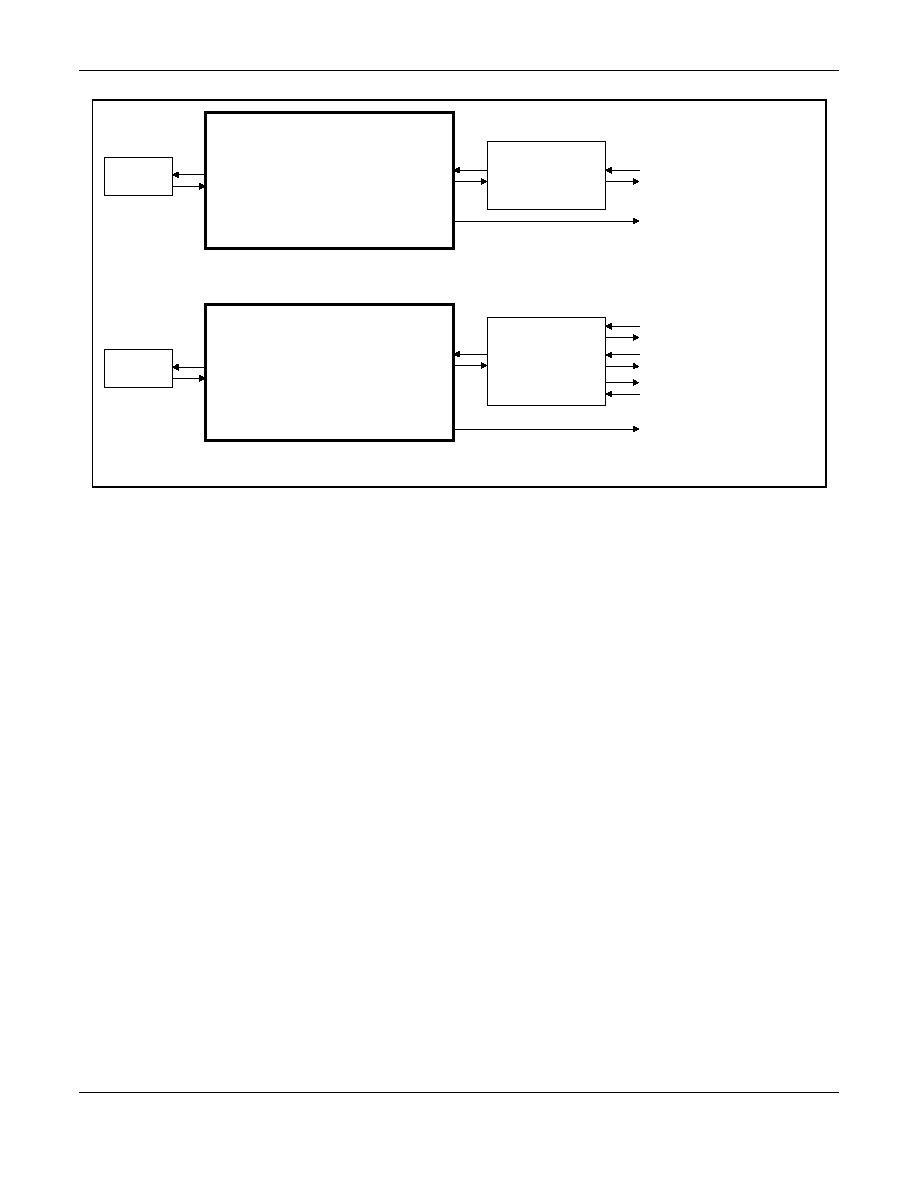
a. Typical Interface for Data/Fax/Remote TAM
b. Typical Interface for Data/Fax/Voice/Speakerphone
RH56D-PCI MODEM DEVICE
C O M B I N E D P C I B U S I N T E R F A C E
A N D M O D E M D A T A P U M P
[R6795-12: 144-PIN TQFP]
PCI BUS
PSTN
TELEPHONE LINE
TELEPHONE LINE/
TELEPHONE HANDSET/
MIC AND SPEAKER
INTERFACE CIRCUIT
RH56D/SP-PCI MODEM DEVICE
C O M B I N E D P C I B U S I N T E R F A C E
A N D M O D E M D A T A P U M P
[R6795-11: 144-PIN TQFP]
PCI BUS
PSTN
TELEPHONE LINE
SPEAKER (OPTIONAL) [SP MODEL]
TELEPHONE LINE/
TELEPHONE HANDSET/
MIC AND SPEAKER
INTERFACE CIRCUIT
MIC (OPTIONAL) [SP MODEL]
HANDSET (OPTIONAL) [SP MODEL]
DIGITAL SPEAKER
(CALL PROGRESS)
DIGITAL SPEAKER
(CALL PROGRESS)
)LJXUH 5+'3&, 0DMRU ,QWHUIDFHV

5+'3&,
9.IOH[0RGHP'HYLFH6HWIRU'HVNWRS$SSOLFDWLRQV
&RQH[DQW
0'
&RQH[DQW 3URSULHWDU\ ,QIRUPDWLRQ
Description
General
The RH56D-PCI modem provides the processing core for
a complete system design featuring data/fax modem,
voice/TAM, and speakerphone support, depending on
specific model (Table 1).
Note: The term, "RH56D-PCI Device Set", refers to the
family of modem models listed in Table 1.
Modem operation, including dialing, call progress,
telephone line interface, telephone handset interface,
audio interface, and host interface functions are supported
and controlled through the command set.
The modem hardware connects to the host processor via
a PCI Bus interface. The OEM adds a crystal circuit,
EEPROM, telephone line interface, telephone handset
interface (optional), and audio interface (optional) to
complete the system.
Host Modem Software
The host modem software performs two distinct tasks:
1. General modem control which includes command
sets, fax Class 1, voice/TAM, speakerphone, error
correction, data compression, and operating system
interface functions.
2. Modem data pump control. Binary executable code
controlling MDP operation is downloaded as required
during operation.
Configurations of the modem software are provided to
support modem models listed in Table 1.
Binary executable modem software is provided for the
OEM.
Data/Fax Modes
As a V.90/K56flex data modem, the modem can receive
data from a digital source using a V.90- or K56flex-
compatible central site modem over the digital telephone
network portion of the PSTN at line speeds up to 56 kbps.
Asymmetrical data transmission supports sending data up
to V.34 rates. This mode can fallback to full-duplex V.34
mode, and to lower rates as dictated by line conditions.
As a V.34 data modem, the modem can operate in 2-wire,
full-duplex, asynchronous modes at line rates up to 33.6
kbps. Data modem modes perform complete handshake
and data rate negotiations. Using V.34 modulation to
optimize modem configuration for line conditions, the
modem can connect at the highest data rate that the
channel can support from 33600 bps down to 2400 bps
with automatic fallback. Automode operation in V.34 is
provided in accordance with PN3320 and in V.32 bis in
accordance with PN2330. All tone and pattern detection
functions required by the applicable ITU or Bell standard
are supported.
In fax modem mode, the modem can operate in 2-wire,
half-duplex, synchronous modes and can support Group 3
facsimile send and receive speeds of 14400, 12000,
9600, 7200, 4800, or 2400 bps. Fax data transmission
and reception performed by the modem are controlled and
monitored through the fax EIA/IA-578 Class 1 and T.31
Class 1.0 command interface. Full HDLC formatting, zero
insertion/deletion, and CRC generation/checking are
provided.
Synchronous Access Mode (SAM) - Video
Conferencing
V.80 synchronous access mode between the modem and
the host/DTE is provided for host-controlled
communication protocols, e.g., H.324 video conferencing
applications.
Voice-call-first (VCF) before switching to a videophone
call is also supported.
Voice/TAM Mode
Voice/TAM Mode features include 8-bit
�
-Law, A-Law, and
linear coding at 8000 Hz and 7200 Hz sample rates. Tone
detection/generation, call discrimination, and concurrent
DTMF detection are also supported. ADPCM (4-bit IMA)
coding is also supported to meet Microsoft WHQL logo
requirements.
Voice/TAM Mode is supported by three submodes:
1. Online Voice Command Mode supports connection to
the telephone line or, for the SP model, a handset.
2. Voice Receive Mode supports recording voice or
audio data input at the RIN pin, typically from the
telephone line or, for the SP model, a
microphone/handset.
3. Voice Transmit Mode supports playback of voice or
audio data to the TXA1/TXA2 output, typically to the
telephone line or, for the SP model, a
speaker/handset.
Speakerphone Mode (SP Model)
The SP model includes additional telephone handset,
external microphone, and external speaker interfaces
which support voice and full-duplex speakerphone (FDSP)
operation.
Hands-free full-duplex telephone operation is supported in
Speakerphone Mode under host control. Speakerphone
Mode features an advanced proprietary speakerphone
algorithm which supports full-duplex voice conversation
with acoustic, line, and handset echo cancellation.
Parameters are constantly adjusted to maintain stability
with automatic fallback from full-duplex to pseudo-duplex
operation. The speakerphone algorithm allows position
independent placement of microphone and speaker. The
host can separately control volume, muting, and AGC in
microphone and speaker channels.
9.IOH[0RGHP'HYLFH6HWIRU'HVNWRS$SSOLFDWLRQV
5+'3&,
0'
&RQH[DQW
&RQH[DQW 3URSULHWDU\ ,QIRUPDWLRQ
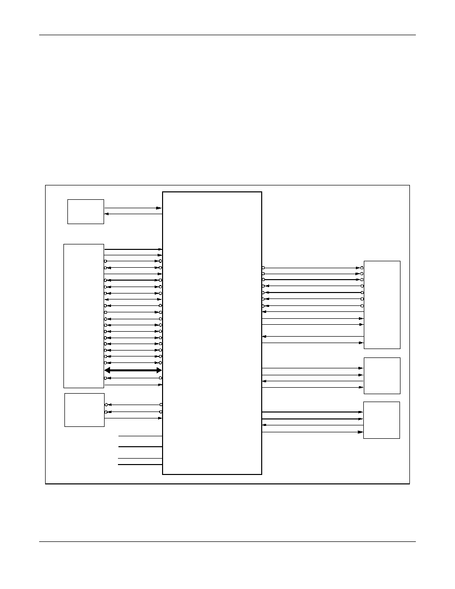
Hardware Interface
The major functional interface signals are shown in Figure
2.
The R6795 144-pin TQFP hardware interface signals are
shown in Figure 3.
The R6795 144-pin TQFP pin signals are shown in Figure
4.
A schematic showing the R6795 interface for a typical
application (data/fax) is shown in Figure 5.
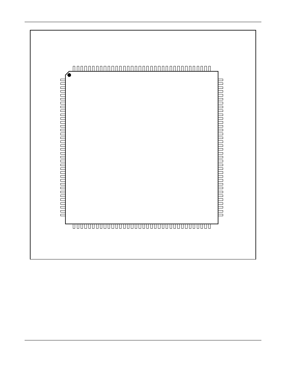
Package Dimensions
The package dimensions for the 144-pin TQFP are shown
in Figure 6.
Power Requirements
The current and power requirements are listed in Table 2.
Absolute Maximum Ratings
The absolute maximum ratings are listed in Table 3.
Additional Information
Additional information is described in the RH56D-PCI
Designer's Guide (Order No. 1213) and in the Command
Reference Manual (Order No. 1118).
MD239F2 R6795 SI
PCI
BUS
PCICLK
PCIRESET#
FRAME#
IDSEL
DEVSEL#
IRDY#
TRDY#
PAR
REQ#
GNT#
INTA#
STOP#
PERR#
SERR#
CBE0#
CBE1#
CBE2#
CBE3#
AD[31:0]
SROMCLK
SROMCS
SROMOUT
SROMIN
AUDIO
INTERFACE
DSPKOUT
SPKOUT*
MIC_V*
SPKMUTE (GPIO8)
XIN
XOUT
28.224 MHZ
CRYSTAL
CIRCUIT
RH56D-PCI
SINGLE DEVICE
MODEM
[R6795: 144-PIN TQFP]
DAA AND
TELEPHONE
INTERFACE
CID# (GPIO1)
VOICE# (GPIO2)
IRING# (INPUT3)
EXT_L# (INPUT4)
LCS_L#/RH_L# (INPUT5)
RXA
TXA1
TXA2
TELIN*
TELOUT*
256 x 16
OR
128 X 16
SERIAL
EEPROM
VDD
AVDD
GND
AGND
+3.3V (VDD)
+3.3VA OR +5VA
GND
AGND
PME#
VpciEN#
VauxEN#
VpciDET
VauxDET
POWER
DETECTION
AND
SWITCHING
CIRCUIT
LCS# (INPUT2)
VIO
* SP MODEL ONLY.
OH# (GPIO0)
)LJXUH 5+'3&, 0DMRU +DUGZDUH ,QWHUIDFH 6LJQDOV

5+'3&,
9.IOH[0RGHP'HYLFH6HWIRU'HVNWRS$SSOLFDWLRQV
&RQH[DQW
0'
&RQH[DQW 3URSULHWDU\ ,QIRUPDWLRQ
XIN
XOUT
AD0
AD1
AD2
AD3
AD4
AD5
AD6
AD7
AD8
AD9
AD10
AD11
AD12
AD13
AD14
AD15
AD16
AD17
AD18
AD19
AD20
AD21
AD22
AD23
AD24
AD25
AD26
AD27
AD28
AD29
AD30
AD31
CBE0#
CBE1#
CBE2#
CBE3#
PCICLK
FRAME#
IDSEL
DEVSEL#
IRDY#
TRDY#
PAR
REQ#
GNT#
INTA#
STOP#
PERR#
SERR#
PME#
PCIRST#
VIO
VIO
VauxDET
VauxEN#
VpciEN#
VpciDET
VDD
VDD
VDD
VDD
VDD
VDD
VDD
VDD
VDD
VDD
VDD
VDD
VDD
VDD
AVDD
AGND
AGND
AGND
AGND
AGNDM
AGNDV/NC*
GND
GND
GND
GND
GND
GND
GND
83
82
44
43
42
41
39
38
37
36
32
31
29
28
27
26
24
23
11
10
9
8
6
5
4
3
138
137
136
134
133
132
131
130
33
22
12
139
126
13
144
16
14
15
21
128
127
123
17
18
19
85
124
1
140
114
116
117
125
2
7
20
25
30
34
40
71
79
81
97
105
115
135
59
54
55
70
78
67
57
35
84
98
113
141
142
143
27pF
5%
28.224
MHz
1M
27pF
5%
PCI BUS
SROMCS
SROMCLK
SROMIN
SROMOUT
RINGWAKE# (INPUT0)
OH# (GPIO0)
CID# (GPIO1)
VOICE# (GPIO2)
LCS# (INPUT2)
IRING# (INPUT3)
EXT_L# (INPUT4)
LCS_L#/RH_L# (INPUT 5)
RXA
TXA1
TXA2
VREF
VC
SPKMUTE (GPIO8)
DSPKOUT
SPKOUT*
MIC_V/NC*
TELIN/NC*
TELOUT/NC*
SLEEPO (GPIO15)
IASLEEP
M_CLK
V_SCLK
M_SCLK
V_STROBE
M_STROBE
V_TXSIN
M_TXSIN
V_RXOUT
M_RXOUT
V_CTRL
M_CTRL
MCTRLSIN
VCTRLSIN/NC*
MRXOUT
VRXOUT/NC*
MTXSIN
VTXSIN/NC*
MSTROBE
VSTROBE/NC*
MSCLK
VSCLK/NC*
MCLKIN
VCLKIN/NC*
GPOL1
GPIO3
GPIO14
INPUT1
NC
SET3V#
CLKRUN#
DRESET# (GPOL0)
RESET#
119
122
121
120
106
104
103
102
108
110
111
112
66
61
62
63
64
100
69
60
65
56
58
46
53
95
88
93
90
91
87
94
89
92
86
96
72
52
76
48
74
50
77
47
75
49
73
51
118
101
99
107
109
80
129
45
68
EEPROM
DAA
AUDIO CIRCUIT
NC
MD239F3 HIS R6795
NC (AVDD = +5V) or
GND (AVDD = +3.3V)
POWER DETECTION AND
SWITCHING CIRCUIT
+3.3V
AGND
+3.3VA or +5VA
GND
10
10
0.1 CER
0.1 CER
FB
RH56D-PCI
R6795
144-PIN TQFP
+3.3V
10K
)LJXUH 5 3LQ 74)3 +DUGZDUH ,QWHUIDFH 6LJQDOV
9.IOH[0RGHP'HYLFH6HWIRU'HVNWRS$SSOLFDWLRQV
5+'3&,
0'
&RQH[DQW
&RQH[DQW 3URSULHWDU\ ,QIRUPDWLRQ
MD239F4 PO R6795 144T
1
2
3
4
5
6
7
8
9
10
11
12
13
14
15
16
17
18
19
20
21
22
23
24
25
26
27
28
29
30
31
32
33
34
35
36
37
38
39
40
41
42
43
44
45
46
47
48
49
50
51
52
53
54
55
56
57
58
59
60
61
62
63
64
65
66
67
68
69
70
71
72
108
107
106
105
104
103
102
101
100
99
98
97
96
95
94
93
92
91
90
89
88
87
86
85
84
83
82
81
80
79
78
77
76
75
74
73
144
143
142
141
140
139
138
137
136
135
134
133
132
131
130
129
128
127
126
125
124
123
122
121
120
119
118
117
116
115
114
113
112
111
110
109
VIO
VDD
AD23
AD22
AD21
AD20
VDD
AD19
AD18
AD17
AD16
CBE2#
FRAME#
IRDY#
TRDY#
DEVSEL#
STOP#
PERR#
SERR#
VDD
PAR
CBE1#
AD15
AD14
VDD
AD13
AD12
AD11
AD10
VDD
AD9
AD8
CBE0#
VDD
GND
AD7
LCS# (INPUT2)
INPUT1
RINGWAKE# (INPUT0)
VDD
OH# (GPIO0)
CID# (GPIO1)
VOICE# (GPIO2)
GPIO3
SPKMUTE (GPIO8)
GPIO14
GND
VDD
M_CTRL
M_CLK
M_TXSIN
M_SCLK
M_RXOUT
M_STROBE
V_STROBE
V_RXOUT
V_SCLK
V_TXSIN
V_CTRL
PME#
GND
XIN
XOUT
VDD
SET3V#
VDD
AGND
MSTROBE
MRXOUT
MSCLK
MTXSIN
MCLKIN
IDSEL
GND
GND
GND
VIO
CBE3#
AD24
AD25
AD26
VDD
AD27
AD28
AD29
AD30
AD31
CLKRUN#
REQ#
GNT#
PCICLK
VpciDET
PCIRST#
INTA#
SROMCLK
SROMIN
SROMOUT
SROMCS
GPOL1
VpciEN#
VauxEN#
VDD
VauxDET
GND
LCS_L#/RH_L# (INPUT5)
EXT_L# (INPUT4)
IRING# (INPUT3)
NC
AD6
AD5
AD4
VDD
AD3
AD2
AD1
AD0
DRESET# (GPOL0)
SLEEPO (GPIO15)
VSTROBE/NC*
VRXOUT/NC*
VSCLK/NC*
VTXSIN/NC*
VCLKIN/NC*
VCTRLSIN/NC*
IASLEEP
AGND
AGND
TELIN/NC*
AGNDV/NC*
TELOUT/NC*
AVDD
SPKOUT/NC*
TXA1
TXA2
VREF
VC
MIC_V/NC*
RXA
AGNDM
RESET#
DSPKOUT
AGND
VDD
MCTRLSIN
* PIN IN NC ON R6795-12
)LJXUH 5 3LQ 74)3 3LQ 6LJQDOV

5+'3&,
9.IOH[0RGHP'HYLFH6HWIRU'HVNWRS$SSOLFDWLRQV
&RQH[DQW
0'
&RQH[DQW 3URSULHWDU\ ,QIRUPDWLRQ
+ 3 . 3 V
+ 3 . 3 V
E E P R O M V C C
VI/O
V C C
V A U X
A N A L O G _ I A _ P O W E R
A D 7
A D 1 5
A D 1 9
I R I N G #
C / B E 3 #
A D 2 5
I N T A #
A D 3 1
P C I R E S E T #
D R E S E T #
I R D Y #
A D 1 2
A D 2 0
A D 2 3
V _ T X S I N
A D 3
M _ C L K
A D 6
A D 2 4
S E R R #
A D 1 0
I A S L E E P
O H #
T R D Y #
C / B E 0 #
M _ T X S I N
T X A 1
D E V S E L #
A D 2
C / B E 1 #
A D 2 2
R X A
T X A 2
V _ C T R L
R I N G W A K E #
A D 2 6
M _ S C L K
V _ S C L K
D R E S E T #
A D 1
A D 9
A D 1 8
A D 2 1
V _ R X O U T
A D 1 6
P A R
A D 2 9
A D 4
A D 1 1
A D 1 3
C / B E 2 #
A D 2 8
A D 3 0
A D 1 7
P E R R #
A D 0
A D 5
A D 1 4
S T O P #
M _ R X O U T
F R A M E #
I D S E L
M _ C T R L
D S P K O U T
S R O M I N
G N T #
V _ S T R O B E
V C
P C I C L K
A D 8
A D 2 7
R E Q #
M _ S T R O B E
V R E F
P C I P M E #
S R O M C L K
S R O M C S
S P E A K M U T E
S R O M O U T
+
C 3 1
1 0 u F
C 3 0
0 . 1 u F
C 2 8
0 . 1 u F
L 2
R 1 5
1 M
Y 1
2 8 . 2 2 4 M H z
C 3 2
2 7 p F
5 %
C 3 3
2 7 p F
5 %
+
C 2 9
1 0 u F
R 1 6
0
I N 1
I N S U L A T O R
for Y1
R 1 2
1 0 K
D 1
B A S 1 6
R6795
5 9
8 9
7 1
8 7
7 9
8 8
8 0
1 1 7
9 3
1 3 0
5 7
7 8
7 0
9 0
1 1 6
9 1
6 7
9 5
1 3 1
1 1 8
1 3 2
1 2 3
9 4
9 2
9 6
1 2 7
1 2 8
4 5
1 3 3
8 3
2 1
1 7
1 3 4
1 8
8 2
1 9
1 3 6
1 3 7
1 3 8
1 3 9
1 1 1
1 1 4
1 1 2
3
4
5
1 2
1 0 6
1 0 7
1 0 8
1 1 0
6
8
9
2 2
1 0
1 1
2 3
2 4
2 6
2 7
2 8
3 3
3 1
3 2
1
3 6
3 7
3 8
3 9
4 1
4 2
4 3
4 4
8 5
1 2 4
1 2 6
1 2 9
1 4 4
1 3
1 4
1 5
1 6
9 9
1 0 1
1 0 3
1 0 4
1 1 9
1 2 0
1 2 1
1 2 2
1 4 0
4 6
7 2
8 6
5 2
7 6
4 8
7 4
5 0
7 7
4 7
4 9
6 9
6 0
6 1
6 2
6 6
6 4
6 3
5 6
5 8
6 5
5 3
6 8
5 4
5 5
1 0 0
1 0 2
105
135
97
81
1 2 5
40
34
30
25
115
20
143
142
141
113
98
84
7
2
35
5 1
1 0 9
7 5
7 3
2 9
A V D D
V _ R X O U T
V D D
V _ T X S I N
V D D
V _ S C L K
S E T 3 V #
G P O H 1 / V p c i E N
M _ S C L K
A D 3 1
A G N D V
A G N D
A G N D
V _ S T R O B E
G P O H 0 / V a u x E N
M _ S T R O B E
A G N D M
M _ C L K
A D 3 0
G P O L 1
A D 2 9
I N T A #
M _ T X S I N
M _ R X O U T
M _ C T R L
G N T #
R E Q #
G P O L 0 / D R E S E T #
A D 2 8
S D X T A L 1 / X I N
P A R
S T O P #
A D 2 7
P E R R #
S D X T A L 2 / X O U T
S E R R #
A D 2 6
A D 2 5
A D 2 4
C B E 3 #
I N P U T 4 / E X T _ L #
I N P U T 7 / V a u x D E T
I N P U T 5 / L C S _ L # / R H _ L #
A D 2 3
A D 2 2
A D 2 1
C B E 2 #
I N P U T 0 / R I N G W A K E #
I N P U T 1
I N P U T 2 / L C S #
I N P U T 3 / I R I N G #
A D 2 0
A D 1 9
A D 1 8
C B E 1 #
A D 1 7
A D 1 6
A D 1 5
A D 1 4
A D 1 3
A D 1 2
A D 1 1
C B E 0 #
A D 9
A D 8
V I O 1
A D 7
A D 6
A D 5
A D 4
A D 3
A D 2
A D 1
A D 0
P M E #
P C I R S T #
P C I C L K
C L K R U N #
I D S E L
F R A M E #
I R D Y #
T R D Y #
D E V S E L #
R E S E T E N / G P I O 1 4
G P I O 3
C I D # / G P I O 1
O H # / G P I O 0
S R O M C S
S R O M O U T
S R O M I N
S R O M C L K
V I O 2
S L E E P O / G P I O 1 5
M C T R L S I N
V _ C T R L
V C T R L S I N
M R X O U T
V R X O U T
M T X S I N
V T X S I N
M S T R O B E
V S T R O B E
V S C K
D S P K O U T
S P K O U T
T X A 1
T X A 2
R X A
V C
V R E F
T E L I N
T E L O U T
M I C _ V
I A S L E E P
R E S E T #
A G N D
A G N D
G P I O 8
V O I C E # / G P I O 2
VDD
VDD
VDD
VDD
V p c i D E T
VDD
VDD
VDD
VDD
VDD
VDD
GND
GND
GND
GND
GND
GND
VDD
VDD
GND
V C L K I N
N C
M S C K
M C L K I N
A D 1 0
R 1 0
1 k
U 3
N M 9 3 C 6 6 M 8
8
6
4
2
7
1
3
5
V D D
P E
D O
S K
P R E
C S
DI
G N D
AD[0..31]
R E Q #
S T O P #
I N T A #
O H #
C / B E 3 #
P E R R #
T X A 2
T X A 1
I R I N G #
C / B E 2 #
D E V S E L #
I D S E L
C / B E 0 #
P A R
I R D Y #
R X A
P C I C L K
G N T #
D S P K O U T
S E R R #
F R A M E #
T R D Y #
P C I R E S E T #
C / B E 1 #
P C I P M E #
S P K O U T
M I C _ V
S P E A K M U T E
Ferrite
F o r L a y o u t : P l a c e V r e f a n d V C
C o m p o n e n t s n e a r U 7 ( R 6 7 9 3 )
R16 Not Installed = +5V IA Operation
R16 Installed = +3.3V IA Operation
1 0 K
V C C
)LJXUH 6FKHPDWLF 5 ,QWHUIDFH �6SHDNHUSKRQH $SSOLFDWLRQ

9.IOH[0RGHP'HYLFH6HWIRU'HVNWRS$SSOLFDWLRQV
5+'3&,
0'
&RQH[DQW
&RQH[DQW 3URSULHWDU\ ,QIRUPDWLRQ
e
b
D
DETAIL A
DETAIL A
A1
L1
c
L
A
D2
D1
D1
A2
Millimeters
0.05
21.75
0.5
0.17
0.11
1.6 MAX
0.15
1.4 REF
22.25
20.0 REF
17.5 REF
0.75
1.0 REF
0.50 BSC
0.27
0.17
0.08 MAX
0.0020
0.8563
0.0197
0.0067
0.0043
A
A1
A2
D
D1
D2
L
L1
e
b
c
Coplanarity
Min.
Max.
Min.
Max.
Inches*
Dim.
Ref: 144-PIN TQFP (GP00-D252)
* Metric values (millimeters) should be used for
PCB layout. English values (inches) are
converted from metric values and may include
round-off errors.
0.0630 MAX
0.0059
0.0551 REF
0.8760
0.7874 REF
0.6890 REF
0.0295
0.0394 REF
0.0197 BSC
0.0106
0.0067
0.0031 MAX
PD-TQFP-144 (040395)
D1
D
D2
D1
PIN 1
REF
)LJXUH 3DFNDJH 'LPHQVLRQV 3LQ 74)3

5+'3&,
9.IOH[0RGHP'HYLFH6HWIRU'HVNWRS$SSOLFDWLRQV
&RQH[DQW
0'
&RQH[DQW 3URSULHWDU\ ,QIRUPDWLRQ
7DEOH &XUUHQW DQG 3RZHU 5HTXLUHPHQWV
Conditions
Current
Power
Device State (Dx)
and Bus State (Bx)
PCI Bus
Power
PCI Clock
(PCICLK)
Line
Connection
Typical
Current (mA)
Maximum
Current (mA)
Typical
Power (mW)
Maximum
Power (mW)
D0, B0
On
Running
Yes
TBD
TBD
TBD
TBD
D0, B0
On
Running
No
TBD
TBD
TBD
TBD
D3, B0
On
Running
No
TBD
TBD
TBD
TBD
D3, B1
On
Running
No
TBD
TBD
TBD
TBD
D3, B2, B3 (D3 hot)
On
Stopped
No
TBD
TBD
TBD
TBD
D3, B3 (D3 cold)
Off
Stopped
No
TBD
TBD
TBD
TBD
Notes:
Operating voltage: VDD = +3.3V � 0.3V.
Test conditions: VDD = +3.3 VDC for typical values; VDD = +3.6 VDC for maximum values.
For all modes, +3.3V is supplied to BIF and MDP.
Definitions:
PCI Bus Power
On: PCI Bus +5V and +3.3V on (modem normally powered by +3.3V from PCI Bus +3.3V
or regulated down from PCI Bus +5V); PCIRST# not asserted.
Off: PCI Bus +5V and +3.3V off (modem normally powered by +3.3V from Vaux or Vpci); PCIRST# asserted.
PCI Clock (PCICLK)
Running: PCI Bus signal PCICLK running;
Stopped: PCI Bus signal PCICLK stopped (off).
Line connection:
Yes: Off-hook, IA powered.
No: On-hook, IA powered down.
Device States:
D3: Low power state. Suspend state can change the system power state; the resulting power state depends
on the system architecture (OS, BIOS, hardware) and system configuration (i.e., other PCI installed cards).
D0: Full power state.
Device and Bus States: D0, B0:
Any PCI transaction, PCICLK running, VCC present.
D3, B1:
No PCI Bus transactions, PCICLK running, VCC present.
D3, B2, B3: No PCI transactions, PCICLK stopped, VCC may be present.
D3, B3:
No PCI transactions, PCICLK stopped, no VCC.
Refer to the PCI Bus Power Management Interface Specification for additional information.
7DEOH $EVROXWH 0D[LPXP 5DWLQJV
Parameter
Symbol
Limits
Units
Supply Voltage
V
DD
-0.5 to +4.0
V
Input Voltage
V
IN
-0.5 to (VIO +0.5)*
V
Operating Temperature Range
T
A
-0 to +70
�C
Storage Temperature Range
T
STG
-55 to +125
�C
Analog Inputs
V
IN
-0.3 to (VAA + 0.5)
V
Voltage Applied to Outputs in High Impedance (Off) State
V
HZ
-0.5 to (VIO +0.5)*
V
DC Input Clamp Current
I
IK
�20
mA
DC Output Clamp Current
I
OK
�20
mA
Static Discharge Voltage (25�C)
V
ESD
�2500
V
Latch-up Current (25�C)
I
TRIG
�400
mA
* VIO = +3.3V � 0.3V or +5V � 5%.

9.IOH[0RGHP'HYLFH6HWIRU'HVNWRS$SSOLFDWLRQV
5+'3&,
0'
&RQH[DQW
&RQH[DQW 3URSULHWDU\ ,QIRUPDWLRQ
NOTES

5+'3&,
9.IOH[0RGHP'HYLFH6HWIRU'HVNWRS$SSOLFDWLRQV
:RUOGZLGH +HDGTXDUWHUV
-DPERUHH 5RDG
32 %R[ &
1HZSRUW %HDFK &$
3KRQH �
)D[
�
)RU PRUH LQIRUPDWLRQ
&DOO
,QWHUQDWLRQDO LQIRUPDWLRQ
&DOO
85/ $GGUHVV
KWWSZZZFRQH[DQWFRP
(0DLO $GGUHVV
OLWHUDWXUH#FRQH[DQWFRP
5(*,21$/ 6$/(6 2)),&(6
86 1RUWKZHVW3DFLILF 1RUWKZHVW
3UXQHULGJH $YHQXH
6XLWH
6DQWD &ODUD &$
3KRQH �
)D[
�
86 /RV $QJHOHV
%XVLQHVV &HQWHU &LUFOH
6XLWH
7KRXVDQG 2DNV &$
3KRQH �
)D[
�
86 6RXWKZHVW
9RQ .DUPDQ $YH
6XLWH
1HZSRUW %HDFK &$
3KRQH �
)D[
�
86 1RUWK &HQWUDO
7ZR 3LHUFH 3ODFH
&KDQFHOORU\ 3DUN
6XLWH
,WDVFD ,/
3KRQH �
)D[
�
86 6RXWK &HQWUDO
3UHVWRQ 5RDG
6XLWH
'DOODV 7;
3KRQH �
)D[
�
86 1RUWKHDVW
/LWWOHWRQ 5RDG
6XLWH $
:HVWIRUG 0$
3KRQH �
)D[
�
86 6RXWKHDVW
3DUNZD\ /DQH 6XLWH
1RUFURVV *$
3KRQH �
)D[
�
86 )ORULGD6RXWK $PHULFD
2QH 3UHVWLJH 3ODFH
0F&RUPLFN 'ULYH
6XLWH
&OHDUZDWHU )/
3KRQH �
)D[
�
86 0LG$WODQWLF
3ULQFHWRQ 3LNH &RUSRUDWH &HQWHU
/HQR[ 'ULYH 6XLWH
/DZUHQFHYLOOH 1-
3KRQH �
)D[
�
(XURSHDQ +HDGTXDUWHUV
/HV 7DLVVRXQLHUHV %
5RXWH GHV 'ROLQHV
%3
6RSKLD $QWLSROLV &HGH[
)UDQFH
3KRQH �
)D[
�
(XURSH &HQWUDO
3DXO*HUKDUGW$OOHH D
0QFKHQ
*HUPDQ\
3KRQH �
)D[
�
(XURSH 0HGLWHUUDQHDQ
9LD * 'L 9LWWRULR
0D]]R 'L 5KR 0,�
,WDO\
3KRQH �
)D[
�
(XURSH 1RUWK
%HUNVKLUH &RXUW
:HVWHUQ 5RDG
%UDFNQHOO
%HUNVKLUH 5* 5(
(QJODQG
3KRQH �
)D[
�
(XURSH 1RUWK 6DWHOOLWH�
*DOJDOH\ +DSODGD 6WUHHW
32 %R[
+HU]OLD
,VUDHO
3KRQH �
)D[
�
(XURSH 6RXWK
7RXU *$1
&HGH[
3DULV /D 'pIHQVH
)UDQFH
3KRQH �
)D[
�
$3$& +HDGTXDUWHUV
.LP 6HQJ 3URPHQDGH
(DVW 7RZHU
*UHDW :RUOG &LW\
6LQJDSRUH
3KRQH �
)D[
�
$XVWUDOLD
6XLWH 5DZVRQ 6WUHHW
(SSLQJ 16:
$XVWUDOLD
3KRQH �
)D[
�
&KLQD
6KDQJKDL 5HSUHVHQWDWLYH 2IILFH
/7 6TXDUH %XLOGLQJ 6XLWH
&KHQJGX 1RUWK 5RDG
6KDQJKDL 35&
3KRQH
)D[
+RQJ .RQJ
WK )ORRU 6XLWHV
+DUERXU &HQWUH
+DUERXU 5RDG
:DQFKDL
+RQJ .RQJ
3KRQH �
)D[
�
,QGLD
5HJLRQDO 2IILFH 6RXWK $VLD
&DSLWDO 7UXVW +RXVH
&RPPXQLW\ &HQWUH
)ULHQGV &RORQ\
1HZ 'HOKL
,QGLD
3KRQH �
)D[
�
.RUHD
5RRP 1R
.RUHD 7H[WLOH &HQWUH %XLOGLQJ
'DHFKLGRQJ
.DQJQDP 32 %R[
.DQJQDPNX
6HRXO
.RUHD
3KRQH �
)D[
�
7DLZDQ +HDGTXDUWHUV
5RRP ,QWHUQDWLRQDO 7UDGH %OGJ
.HHOXQJ 5RDG 6HFWLRQ ,
7DLSHL
7DLZDQ
52&
3KRQH �
)D[
�
-DSDQ +HDGTXDUWHUV
6KLPRPRWR %OGJ
+DWVXGDL 6KLEX\DNX
7RN\R
-DSDQ
3KRQH �
)D[
�
628'