
Data Sheet
Preliminary
Doc. No. MD233
Rev. 2, July 9, 1999
RL56CSMV/3 and RL56CSM/3
AnyPortTM Multi-Service Access Processor
The RL56CSMV/3 and RL56CSM/3 are members of the Conexant
TM
AnyPortTM family of
multi-service access processors, and provide a complete solution to the transport of
multiple media types between circuit-switched remote access and a variety of back-end
networks (Table 1). AnyPort processors are ideally suited for the network infrastructures
resulting from the convergence of voice and data networking, addressing new
requirements such as Voice and Fax over packet networks, ISDN and Cellular Data, while
maintaining support of traditional PSTN Data/Fax needs.
Note: RL56CSMV/3 and CSMV/3 refer to both RL56CSMV/3 and RL56CSM/3 except as
noted. Any reference to voice applies only to the RL56CSMV/3.
The CSMV/3 transcends existing modem solutions by providing a complete system
solution for multi-service remote access. The combined DSP/RISC architecture provides
an ideal engine to run Conexant's extensive suite of field-proven modulations, echo
cancellers, voice coders, and communications protocols. In addition, performing
functions such as T.38, V.120, async-to-sync HDLC conversion for PPP, V.110, and
synchronous HDLC for PPP on ISDN connections, in the access processor allows system
designers to reduce system overhead and increase scalability.
The CSMV/3 is a low-power system providing three communication channels in a single
package. Powerful and downloadable DSP-based data pumps employ on-chip SRAM to
allow upgrades to future voice and communication modulation schemes. An advanced
RISC microcontroller manages three data pumps simultaneously. An innovative host
interface to the Multi-Service Access Processor system uses a shared SDRAM memory
to increase data throughput while reducing system cost and space. A programmable time
slot selection feature provides direct digital connection to a T1/E1/PRI framing device.
A 35mm BGA package houses the CSMV/3 with extra balls available for thermal vias to
minimize heat. A built-in phase lock loop (PLL) minimizes board noise while easing
design. A quick-wake, sleep mode further reduces the power of this +3.3V access
processor system.
Features
Generic
�
Three access channels in one package
�
+3.3V operation with +5V tolerant inputs
�
Downloadable controller firmware and data
pump code
�
Advanced RISC Machines (ARM) architecture
�
Low-power sleep mode with quick wake
�
Glueless interface to Bt8370 T1/E1/PRI framer
with time slot selection
�
Built-in phase lock loop (PLL)
Signaling
�
DTMF detection and generation
�
Multi-frequency tone support for legacy
network equipment (R1 and R2)
Data
�
Data modem modes
-
PSTN: ITU-T V.90, K56flex, K56Plus, V.34
(33.6 kbps), V.FC, V.32 bis, V.32, V.22 bis,
V.22A/B, V.23, and V.21; Bell 212A and 103
-
ISDN: 64/56 kbps ISDN Basic Rate Interface
B Channel HDLC control, or data pass-
through mode for HDLC processing
elsewhere in the central site system
�
Internal error correction and data compression
(ECC)
-
V.42 LAPM and MNP 2-4 error correction
-
V.42 bis and MNP 5 data compression
-
MNP 10EC
TM
enhanced cellular
�
Async/sync HDLC conversion
�
V.120 ISDN data
�
V.110 cellular data
�
LAP-B X.75
Voice (RL56CSMV/3 only)
�
Baseline configuration:
-
G.723.1 and G.723.1 Annex A
-
G.711
�
-law and A-law
-
G.729 Annex A and Annex B
-
G.168 128 ms Network Echo Canceller
�
Patented robust jitter buffer
�
Voice API using Mailbox Messages
FAX
�
Fax modem send and receive rates up to 14.4 kbps
�
V.17, V.33, V.29, V.27 ter, and V.21 channel 2,
Group 3, T.30 protocol and Class 1, 2
supported
�
T.38 real-time fax protocol
Communications software-compatible
AT commands

RL56CSMV/3 and RL56CSM/3
AnyPortTM Multi-Service Access Processor
2
Conexant
MD233
Table 1. RL56CSMV/3 Family Models and Functions
Model/Order/Part Numbers
Supported Functions
Marketing Model Number
Part Number (340-Pin BGA)
Data
Fax
Voice
RL56CSM/3
R7138-94
Yes
Yes
No
RL56CSMV/3
R7178-24
Yes
Yes
Yes
MD233F1 CSMV/3 IF
MCU_CLKIN
+5V
+3.3V
GND
POWER
SUPPLY
A_SCLK
A_FSYNC
A_RXDATA
A_TXDATA
A_TSAEN#
RL56CSMV/3
CH B
ADDRESS (5)
DATA (16)
CONTROL
STATUS
1Mbit x 16
SDRAM
MEMORY BUS (MB)
CH A
CUSTOMER
SYSTEM
CONTROLLER
RL56DDP
DIGITAL
DATA
PUMP
(DDP)
B_SCLK
B_FSYNC
B_RXDATA
B_TXDATA
B_TSAEN#
RL56DDP
DIGITAL
DATA
PUMP
(DDP)
MICRO
CONTROLLER
UNIT
(MCU)
MCU
CLOCK
T1/E1
OR
PRIMARY RATE
LINE INTERFACE
T1/E1
TRANSCEIVER/
FRAMER
(BROOKTREE
Bt8370
OR EQUIVALENT)
SCLK
FSYNC
RXDATA
TXDATA
CH C
C_SCLK
C_FSYNC
C_RXDATA
C_TXDATA
C_TSAEN#
RL56DDP
DIGITAL
DATA
PUMP
(DDP)
HOST BUS (HB)
DP_CLKIN
DDP
CLOCK
VGG
VDD
GND
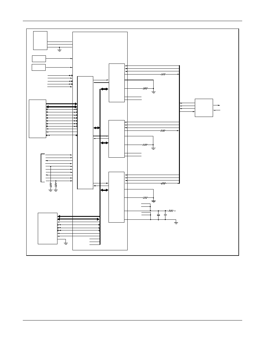
Figure 1. RL56CSMV/3 Implementation Example Block Diagram
Information provided by Conexant Systems, Inc. is believed to be accurate and reliable. However, no responsibility is assumed by Conexant for its use, nor any
infringement of patents or other rights of third parties which may result from its use. No license is granted by implication or otherwise under any patent rights of
Conexant other than for circuitry embodied in Conexant products. Conexant reserves the right to change circuitry at any time without notice. This document is
subject to change without notice.
Conexant products are not designed or intended for use in life support appliances, devices, or systems where malfunction of a Conexant product can reasonably be
expected to result in personal injury or death. Conexant customers using or selling Conexant products for use in such applications do so at their own risk and agree
to fully indemnify Conexant for any damages resulting from such improper use or sale.
Product names or services listed in this publication are for identification purposes only, and may be trademarks or registered trademarks of their respective
companies. All other marks mentioned herein are the property of their respective owners.
K56flex is a trademark of Conexant Systems, Inc. and Lucent Technologies.
Conexant, "What's Next in Communications Technologies", AnyPort, and MNP10 EC are trademarks of Conexant Systems, Inc.
�1999, Conexant Systems, Inc.
All Rights Reserved.

AnyPortTM Multi-Service Access Processor
RL56CSMV/3 and RL56CSM/3
MD233
Conexant
3
Technical Specifications
General Description
The CSMV/3 provides the processing core for three
channels of a central site Remote Access Server
supporting high speed T1/E1/PRI digital lines. The OEM
adds two oscillators, SDRAM, and discrete components
to complete the Multi-Service Access Processor system.
The access processor includes a full-featured, self-
contained data/fax/Voice modem solution shown in Figure
1. Data modem handshake, fax modem protocol, voice
codecs, and ISDN data connection functions are
supported and controlled through the AT command set.
Digital Data Pump (DDP)
The DDP is a +3.3V Conexant data pump supporting
PSTN data/fax modem operation, ISDN B Channel call
termination mode, and voice coding/decoding. The DDP
executes internal code including downloadable modules
from on-chip memory.
Digital data transfers serially between the T1/E1 framer
device and the DDP at a data rate up to 8.192 Mbps. The
T1/E1 framing device provides a strobe signal and the
DDP TSA logic detects where the data for the channel
starts in the serial TDM data stream using a
programmable counter. The DDP performs PCM �-law or
A-law conversion and synchronizes with an external
network clock.
ARM Microcontroller (MCU)
The ARM MCU performs the command processing and
interfaces to the central site system controller via a 16-bit
parallel host interface. Two 64-word deep FIFOs are used
for improved data throughput between the access
processor and system controller. This single powerful
RISC processor controls three separate channels. A
SDRAM loader is available to support download from the
central site system controller on startup, if desired.
Access Processor Operation
In data modem modes, each channel can independently
connect to PSTN data modems at rates up to 56 kbps or
ISDN terminal adapters at rates up to 64 kbps. A
downloadable architecture allows for software download.
For PSTN modems, complete handshake and data rate
negotiations are performed. By optimizing the modem
configuration for line conditions, the DDP can connect at
the highest data rate that the channel can support from
56 kbps to 300 bps with automatic fallback. Automode
operation in V.34 is provided in accordance with PN3320
and in V.32 bis in accordance with PN2330. All tone and
pattern detection functions required by the applicable ITU
or Bell standard are supported. Asynchronous to
synchronous conversion is supported inside the controller
to ease PPP processing in PSTN data mode.
When the remote end is an ISDN terminal adapter, the
CSMV/3 provides HDLC control including HDLC Flag
generation/detection, bit stuffing/extraction, and CRC
generation/checking. V.120, V.110, and LAP-B X.75 are
also supported. V.120 is a standard for encapsulating
asynchronous data communications traffic into ISDN data
streams.
In fax modem mode, the CSMV/3 supports Group 3
facsimile send and receive speeds of 14400, 12000,
9600, 7200, 4800, and 2400 bps Fax modem modes
support T.30 and T.38 fax requirements. Fax data
transmission and reception performed by the access
processor are controlled and monitored through the EIA-
578 Class 1 and Class 2 command interface. Both
transmit and receive fax data are buffered within the
access processor.
In Voice mode, the CSMV/3 encodes PCM audio data
from the line into Real-Time Protocol (RTP) packets for
the Host, and decodes RTP packets from the Host, to
output PCM audio data to the line. In Voice mode, DTMF
digits can be detected and transmitted, and a Voice
Activity Detector can be enabled.
Access Processor Firmware
Access processor firmware performs processing of
general modem control, command sets, error correction
and data compression, fax class 1 and class 2, voice
coding and decoding (optional), and central site system
controller interface functions.
The firmware is provided in object code form for
executing from external SDRAM after download on
startup using the ROM-coded Boot Loader. Equipment
designers can add their own functions in firmware using
commonly available development tools and the C
programming language.
Hardware Interface Signals
The RL56CSMV/3 interface is illustrated in Figure 2.
The 340-pin BGA package identifying pin locations for the
RL56CSMV/3 is shown in Figure 3.
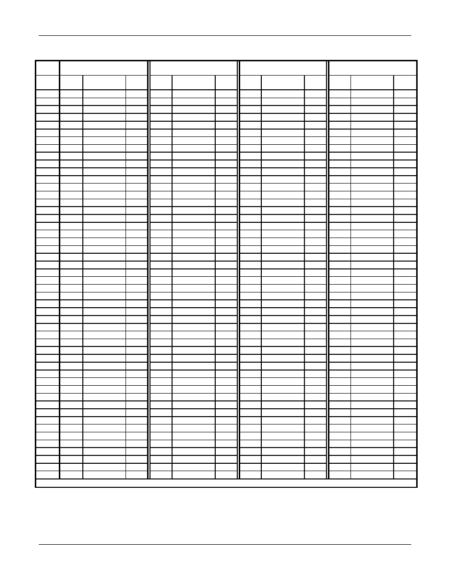
The RL56CSMV/3 pin signals in the 340-pin BGA are
listed by location in Table 2 and by interface in Table 3.
Additional Information
Additional information is described in the RL56CSMV/3
and RL56CSM/3 AnyPort Multi-Service Access Processor
Hardware Interface Description (Order No. 1137), the
RL56DDP Designer's Guide (Order No. 1141), the CSM/3
and CSMV/3 AnyPortTM Multi-Service Access Processor
Software Interface Description (Order No. 1148), and the
Command Reference Manual (Order No. 1195).
RL56CSMV/3 and RL56CSM/3
AnyPortTM Multi-Service Access Processor
4
Conexant
MD233
1137F3-1 CSM/3 HWIF
A[12:1]
D[15:0]
MCU_CLKOUT
RW#
RAS#
CAS#
BS0
BS1
POWER
SUPPLY
RL56CSMV/3
MCU_CLKIN
DP_CLKIN
MCU_RESET#
ROME
MCU_TEST#
DP_TEST#
XYCNT
HBA[5:1]
HBD[15:0]
HBCLK
HBEN#
HBCS#
HBRD#
HBWR#
HBACKR#
HBACKW#
HBRQSTR
HBRQSTW
HBIRQ#
SDRAM
MEMORY BUS (MB)
CUSTOMER
SYSTEM
CONTROLLER
HOST
INTERFACE
MICRO
CONTROLLER
UNIT
(MCU)
DP
CLOCK
T1/E1
OR
PRIMARY RATE
LINE INTERFACE
T1/E1
TRANSCEIVER/
FRAMER
(BROOKTREE
Bt8370
OR EQUIVALENT)
SCLK
FSYNC
RXDATA
TXDATA
RL56DDP
DIGITAL
DATA
PUMP
(DDP)
HOST BUS (HB)
MCU
CLOCK
VDD
VGG
GND
RL56DDP
DIGITAL
DATA
PUMP
(DDP)
A_PLLVDD
B_PLLVDD
C_PLLVDD
A_PLLGND
B_PLLGND
C_PLLGND
RL56DDP
DIGITAL
DATA
PUMP
(DDP)
JTAG
+3.3V
+5V
GND
WR#
RD#
CS1
A[11:0]
D[15:0]
CLK
WE#
RAS#
CAS#
DQML
DQMU
CS#
NC
NC
NC
0.1
10 TANT
VDD
+
10
CH A
A_SCLK
A_FSYNC
A_RXDATA
A_TXDATA
A_TSAEN#
A_DPRST#
A_PLLVDD
A_PLLGND
20K
33
CH B
B_SCLK
B_FSYNC
B_RXDATA
B_TXDATA
B_TSAEN#
B_DPRST#
B_PLLVDD
B_PLLGND
20K
33
CH C
C_SCLK
C_FSYNC
C_RXDATA
C_TXDATA
C_TSAEN#
C_DPRST#
20K
33
TCK
TDI
TDO
TMS
TRST#
DPBS_TCLK
DPBS_TDI
DPBS_TDO
DPBS_TMS
DPBS_TRST#
3K
3K
Figure 2. RL56CSMV/3 Hardware Interface Signals

AnyPortTM Multi-Service Access Processor
RL56CSMV/3 and RL56CSM/3
MD233
Conexant
5
PIN A1 CORNER
26
25
24
23
22
21
20
19
18
17
16
15
14
13
12
11
10
9
8
7
6
5
4
3
2
1
A
B
C
D
E
F
G
H
J
K
L
M
N
P
R
T
U
V
W
Y
AA
AB
AC
AD
AE
AF
TOP VIEW
BOTTOM VIEW
MD194F4 268BGA
Figure 3. 340-Pin BGA Package

RL56CSMV/3 and RL56CSM/3
AnyPortTM Multi-Service Access Processor
6
Conexant
MD233
Table 2. RL56CSMV/3 Pin Signals by Pin Location
Table
Col.
1
2
3
4
Table
Row
Loc.
Signal
I/F
Loc.
Signal
I/F
Loc.
Signal
I/F
Loc.
Signal
I/F
1
A01
C_DPRST#
GND thru
20K
B25
B_DPRXCLK
TEST
F03
VDD
3.3V
K25
A_DPTXCLK
TEST
2
A02
A_DPRST#
GND thru
20K
B26
RESERVED
F05
RESERVED
K26
A_RXDATA
CH A
3
A03
B_DPRST#
GND thru
20K
C01
B_RXDATA
CH B
F06
GND
GND
L01
D9
MB
4
A04
VGG
5V
C02
RESERVED
F07
GND
GND
L02
D8
MB
5
A05
B_DPCS
TEST
C03
RESERVED
F08
GND
GND
L03
B_EYEXY
CH B
6
A06
A4
MB
C04
RESERVED
F19
GND
GND
L24
XYCNT
TEST
7
A07
A3
MB
C05
VDD
3.3V
F20
GND
GND
L25
RESERVED
8
A08
A2
MB
C06
B_YCLK
CH B
F21
GND
GND
L26
A_TXDATA
CH A
9
A09
A1
MB
C07
B_XCLK
CH B
F22
RESERVED
M01
D12
MB
10
A10
A0
MB
C08
B_DSPRST
TEST
F24
DP_TEST#
TEST
M02
D11
MB
11
A11
D7
MB
C09
B_PLLGND
CH B
F25
RESERVED
M03
D10
MB
12
A12
D6
MB
C10
RESERVED
F26
A_EYESYNC
CH A
M24
VDD
3.3V
13
A13
D5
MB
C11
DPBS_TRST#
JTAG
G01
B_EYESYNC
CH B
M25
A_DPCS
TEST
14
A14
D0
MB
C12
VDD
3.3V
G02
RESERVED
M26
A_DSPRST
TEST
15
A15
DP_CLKIN
SYS
C13
B_DPINT
TEST
G03
B_PLLVDD
CH B
N01
D15
MB
16
A16
RESERVED
C14
RESERVED
G05
RESERVED
N02
D14
MB
17
A17
A_DPINT
TEST
C15
VDD
3.3V
G06
GND
GND
N03
D13
MB
18
A18
A_DSPINT
TEST
C16
A_PLLVDD
CH A
G07
GND
GND
N24
WR#
MB
19
A19
A_EYEXY
CH A
C17
RESERVED
G08
GND
GND
N25
A_PLLGND
CH A
20
A20
A_XCLK
CH A
C18
RESERVED
G19
GND
GND
N26
DPBS_TCLK
JTAG
21
A21
A_YCLK
CH A
C19
RESERVED
G20
GND
GND
P01
CAS#
MB
22
A22
RESERVED
C20
RESERVED
G21
GND
GND
P02
RAS#
MB
23
A23
A_TSAEN#
CH A
C21
RESERVED
G22
RESERVED
P03
MCU_CLKIN
SYS
24
A24
RESERVED
C22
RESERVED
G24
RESERVED
P24
C_DSPINT
TEST
25
A25
RESERVED
C23
A_DPTXD
TEST
G25
RESERVED
P25
RD#
MB
26
A26
RESERVED
C24
VDD
3.3V
G26
A_SCLK
CH A
P26
C_EYEXY
CH C
27
B01
B_TXDATA
CH B
C25
RESERVED
H01
B_EYECLK#
CH B
R01
PA5
NA
28
B02
RESERVED
C26
RESERVED
H02
RESERVED
R02
RESERVED
29
B03
RESERVED
D01
RESERVED
H03
B_DSPINT
TEST
R03
MCU_CLKOUT
MB
30
B04
RESERVED
D02
RESERVED
H05
RESERVED
R24
C_DPTXCLK
TEST
31
B05
RESERVED
D03
RESERVED
H06
GND
GND
R25
C_YCLK
CH C
32
B06
RESERVED
D24
VDD
3.3V
H07
GND
GND
R26
C_XCLK
CH C
33
B07
C_DPEXRST
TEST
D25
A21
MB
H08
GND
GND
T01
PA3
NA
34
B08
A_DPEXRST
TEST
D26
RESERVED
H19
GND
GND
T02
PE4
NA
35
B09
B_DPEXRST
TEST
E01
B_FSYNC
CH B
H20
GND
GND
T03
VDD
3.3V
36
B10
D4
MB
E02
RESERVED
H21
GND
GND
T24
C_DPINT
TEST
37
B11
D3
MB
E03
RESERVED
H22
RESERVED
T25
VDD
3.3V
38
B12
D2
MB
E05
RESERVED
H24
VDD
3.3V
T26
VDD
3.3V
39
B13
D1
MB
E06
RESERVED
H25
RESERVED
U01
PA7
NA
40
B14
C_DPRXD
TEST
E07
RESERVED
H26
A_FSYNC
CH A
U02
PE0
NA
41
B15
RESERVED
E08
RESERVED
J01
RESERVED
U03
VDD
3.3V
42
B16
RESERVED
E19
RESERVED
J02
B_TSAEN#
CH B
U24
VGG
5V
43
B17
RESERVED
E20
RESERVED
J03
VDD
3.3V
U25
C_TSAEN#
CH C
44
B18
A_DPRXD
TEST
E21
RESERVED
J24
RESERVED
U26
RESERVED
45
B19
RESERVED
E22
RESERVED
J25
RESERVED
V01
PE6
NA
46
B20
RESERVED
E24
RESERVED
J26
RESERVED
V02
PE2
NA
47
B21
RESERVED
E25
RESERVED
K01
BS1
MB
V03
RESERVED
48
B22
B_DPRXD
TEST
E26
A_EYECLK#
CH A
K02
DPBS_TDO
JTAG
V24
C_DPRXCLK
TEST
49
B23
B_DPTXD
TEST
F01
B_SCLK
CH B
K03
VDD
3.3V
V25
C_DPTXD
TEST
50
B24
B_DPTXCLK
TEST
F02
RESERVED
K24
A_DPRXCLK
TEST
V26
C_PLLVDD
CH C
Notes: RESERVED = May have internal circuit connected, no external connection allowed.
AnyPortTM Multi-Service Access Processor
RL56CSMV/3 and RL56CSM/3
MD233
Conexant
7
Table 2. RL56CSMV/3 Pin Signals by Pin Location (Continued)
Table
Col.
5
6
7
8
Table
Row
Loc.
Signal
I/F
Loc.
Signal
I/F
Loc.
Signal
I/F
Loc.
Signal
I/F
1
W01
PA4
NA
AB20
RESERVED
AE13
HBA1
HB
2
W02
PA6
NA
AB21
RESERVED
AE14
HBCS#
HB
3
W03
VDD
3.3V
AB22
RESERVED
AE15
HBWR#
HB
4
W05
GND
GND
AB24
RESERVED
AE16
HBCLK
HB
5
W06
GND
GND
AB25
C_FSYNC
CH C
AE17
HBEN#
HB
6
W07
GND
GND
AB26
CS3
MB
AE18
A5
MB
7
W08
GND
GND
AC01
TRST#
JTAG
AE19
A7
MB
8
W19
GND
GND
AC02
PF3
NA
AE20
A9
MB
9
W20
GND
GND
AC03
VDD
3.3V
AE21
A13
MB
10
W21
GND
GND
AC24
CS0
MB
AE22
VDD
3.3V
11
W22
RESERVED
AC25
C_TXDATA
CH C
AE23
RESERVED
12
W24
MCU_RESET#
SYS
AC26
C_SCLK
CH C
AE24
A14
MB
13
W25
ROME
SYS
AD01
PF7
NA
AE25
A22
MB
14
W26
BS0
MB
AD02
TMS
JTAG
AE26
A24
MB
15
Y01
PE1
NA
AD03
VDD
3.3V
AF01
PF4
NA
16
Y02
PE3
NA
AD04
VDD
3.3V
AF02
PF6
NA
17
Y03
VDD
3.3V
AD05
VDD
3.3V
AF03
TDI
JTAG
18
Y05
GND
GND
AD06
VDD
3.3V
AF04
HBACKR#
HB
19
Y06
GND
GND
AD07
VDD
3.3V
AF05
HBACKW#
HB
20
Y07
GND
GND
AD08
VDD
3.3V
AF06
HBD0
HB
21
Y08
GND
GND
AD09
VDD
3.3V
AF07
HBD2
HB
22
Y19
GND
GND
AD10
VDD
3.3V
AF08
HBD3
HB
23
Y20
GND
GND
AD11
VDD
3.3V
AF09
HBD10
HB
24
Y21
GND
GND
AD12
HBD14
HB
AF10
HBD8
HB
25
Y22
RESERVED
AD13
HBA2
HB
AF11
HBD5
HB
26
Y24
C_EYECLK#
CH C
AD14
HBA5
HB
AF12
HBD13
HB
27
Y25
MCU_TEST#
SYS
AD15
DPBS_TDI
JTAG
AF13
HBD11
HB
28
Y26
CS4
MB
AD16
C_PLLGND
CH C
AF14
HBA3
HB
29
AA01
PE5
NA
AD17
C_DSPRST
TEST
AF15
HBA4
HB
30
AA02
PE7
NA
AD18
A12
MB
AF16
HBRD#
HB
31
AA03
VDD
3.3V
AD19
C_DPCS
TEST
AF17
RESERVED
32
AA05
GND
GND
AD20
A11
MB
AF18
HBIRQ#
HB
33
AA06
GND
GND
AD21
A16
MB
AF19
A6
MB
34
AA07
GND
GND
AD22
A15
MB
AF20
DPBS_TMS
JTAG
35
AA08
GND
GND
AD23
A20
MB
AF21
A8
MB
36
AA19
GND
GND
AD24
RW#
MB
AF22
A10
MB
37
AA20
GND
GND
AD25
C_RXDATA
CH C
AF23
A17
MB
38
AA21
GND
GND
AD26
CS1
MB
AF24
A19
MB
39
AA22
RESERVED
AE01
PF5
NA
AF25
A18
MB
40
AA24
VGG
5V
AE02
TDO
JTAG
AF26
A23
MB
41
AA25
C_EYESYNC
CH C
AE03
TCK
JTAG
42
AA26
CS2
MB
AE04
HBRQSTR
HB
43
AB01
PF0
NA
AE05
HBRQSTW
HB
44
AB02
PF2
NA
AE06
HBD1
HB
45
AB03
PF1
NA
AE07
HBD9
HB
46
AB05
GND
GND
AE08
HBD4
HB
47
AB06
GND
GND
AE09
HBD6
HB
48
AB07
GND
GND
AE10
HBD7
HB
49
AB08
GND
GND
AE11
HBD12
HB
50
AB19
RESERVED
AE12
HBD15
HB
Notes: RESERVED = May have internal circuit connected, no external connection allowed.

RL56CSMV/3 and RL56CSM/3
AnyPortTM Multi-Service Access Processor
8
Conexant
MD233
Table 3. RL56CSMV/3 Pin Signals by Interface
Table
Col.
1
2
3
4
Table
Row
Loc.
Signal
I/F
Loc.
Signal
I/F
Loc.
Signal
I/F
Loc.
Signal
I/F
1
AE13
HBA1
HB
G01
B_EYESYNC
CH B
L02
D8
MB
K25
A_DPTXCLK
TEST
2
AD13
HBA2
HB
H01
B_EYECLK#
CH B
L01
D9
MB
C23
A_DPTXD
TEST
3
AF14
HBA3
HB
J02
B_TSAEN#
CH B
M03
D10
MB
A18
A_DSPINT
TEST
4
AF15
HBA4
HB
C07
B_XCLK
CH B
M02
D11
MB
M26
A_DSPRST
TEST
5
AD14
HBA5
HB
C06
B_YCLK
CH B
M01
D12
MB
A05
B_DPCS
TEST
6
AF06
HBD0
HB
AC26
C_SCLK
CH C
N03
D13
MB
B09
B_DPEXRST
TEST
7
AE06
HBD1
HB
AB25
C_FSYNC
CH C
N02
D14
MB
C13
B_DPINT
TEST
8
AF07
HBD2
HB
AD25
C_RXDATA
CH C
N01
D15
MB
B25
B_DPRXCLK
TEST
9
AF08
HBD3
HB
AC25
C_TXDATA
CH C
W26
BS0
MB
B22
B_DPRXD
TEST
10
AE08
HBD4
HB
V26
C_PLLVDD
CH C
K01
BS1
MB
B24
B_DPTXCLK
TEST
11
AF11
HBD5
HB
AD16
C_PLLGND
CH C
AC24
CS0
MB
B23
B_DPTXD
TEST
12
AE09
HBD6
HB
P26
C_EYEXY
CH C
AD26
CS1
MB
H03
B_DSPINT
TEST
13
AE10
HBD7
HB
AA25
C_EYESYNC
CH C
AA26
CS2
MB
C08
B_DSPRST
TEST
14
AF10
HBD8
HB
Y24
C_EYECLK#
CH C
AB26
CS3
MB
F24
DP_TEST#
TEST
15
AE07
HBD9
HB
U25
C_TSAEN#
CH C
Y26
CS4
MB
L24
XYCNT
TEST
16
AF09
HBD10
HB
R26
C_XCLK
CH C
P25
RD#
MB
A01
C_DPRST#
GND thru
20K
17
AF13
HBD11
HB
R25
C_YCLK
CH C
AD24
RW#
MB
A02
A_DPRST#
GND thru
20K
18
AE11
HBD12
HB
A10
A0
MB
N24
WR#
MB
A03
B_DPRST#
GND thru
20K
19
AF12
HBD13
HB
A09
A1
MB
P02
RAS#
MB
T01
PA3
NA
20
AD12
HBD14
HB
A08
A2
MB
P01
CAS#
MB
W01
PA4
NA
21
AE12
HBD15
HB
A07
A3
MB
R03
MCU_CLKOUT
MB
R01
PA5
NA
22
AE16
HBCLK
HB
A06
A4
MB
P03
MCU_CLKIN
SYS
W02
PA6
NA
23
AE17
HBEN#
HB
AE18
A5
MB
A15
DP_CLKIN
SYS
U01
PA7
NA
24
AE14
HBCS#
HB
AF19
A6
MB
W24
MCU_RESET#
SYS
U02
PE0
NA
25
AF16
HBRD#
HB
AE19
A7
MB
W25
ROME
SYS
Y01
PE1
NA
26
AE15
HBWR#
HB
AF21
A8
MB
Y25
MCU_TEST#
SYS
V02
PE2
NA
27
AF04
HBACKR#
HB
AE20
A9
MB
AE03
TCK
JTAG
Y02
PE3
NA
28
AF05
HBACKW#
HB
AF22
A10
MB
AF03
TDI
JTAG
T02
PE4
NA
29
AE04
HBRQSTR
HB
AD20
A11
MB
AE02
TDO
JTAG
AA01
PE5
NA
30
AE05
HBRQSTW
HB
AD18
A12
MB
AD02
TMS
JTAG
V01
PE6
NA
31
AF18
HBIRQ#
HB
AE21
A13
MB
AC01
TRST#
JTAG
AA02
PE7
NA
32
G26
A_SCLK
CH A
AE24
A14
MB
N26
DPBS_TCLK
JTAG
AB01
PF0
NA
33
H26
A_FSYNC
CH A
AD22
A15
MB
AD15
DPBS_TDI
JTAG
AB03
PF1
NA
34
K26
A_RXDATA
CH A
AD21
A16
MB
K02
DPBS_TDO
JTAG
AB02
PF2
NA
35
L26
A_TXDATA
CH A
AF23
A17
MB
AF20
DPBS_TMS
JTAG
AC02
PF3
NA
36
C16
A_PLLVDD
CH A
AF25
A18
MB
C11
DPBS_TRST#
JTAG
AF01
PF4
NA
37
N25
A_PLLGND
CH A
AF24
A19
MB
AD19
C_DPCS
TEST
AE01
PF5
NA
38
A19
A_EYEXY
CH A
AD23
A20
MB
B07
C_DPEXRST
TEST
AF02
PF6
NA
39
F26
A_EYESYNC
CH A
D25
A21
MB
T24
C_DPINT
TEST
AD01
PF7
NA
40
E26
A_EYECLK#
CH A
AE25
A22
MB
V24
C_DPRXCLK
TEST
C05
VDD
3.3V
41
A23
A_TSAEN#
CH A
AF26
A23
MB
B14
C_DPRXD
TEST
C12
VDD
3.3V
42
A20
A_XCLK
CH A
AE26
A24
MB
R24
C_DPTXCLK
TEST
C15
VDD
3.3V
43
A21
A_YCLK
CH A
A14
D0
MB
V25
C_DPTXD
TEST
C24
VDD
3.3V
44
F01
B_SCLK
CH B
B13
D1
MB
P24
C_DSPINT
TEST
D24
VDD
3.3V
45
E01
B_FSYNC
CH B
B12
D2
MB
AD17
C_DSPRST
TEST
F03
VDD
3.3V
46
C01
B_RXDATA
CH B
B11
D3
MB
M25
A_DPCS
TEST
H24
VDD
3.3V
47
B01
B_TXDATA
CH B
B10
D4
MB
B08
A_DPEXRST
TEST
J03
VDD
3.3V
48
G03
B_PLLVDD
CH B
A13
D5
MB
A17
A_DPINT
TEST
K03
VDD
3.3V
49
C09
B_PLLGND
CH B
A12
D6
MB
K24
A_DPRXCLK
TEST
M24
VDD
3.3V
50
L03
B_EYEXY
CH B
A11
D7
MB
B18
A_DPRXD
TEST
T03
VDD
3.3V
Notes: RESERVED = May have internal circuit connected, no external connection allowed.

AnyPortTM Multi-Service Access Processor
RL56CSMV/3 and RL56CSM/3
MD233
Conexant
9
Table 3. RL56CSMV/3 Pin Signals by Interface (Continued)
Table
Col.
5
6
7
8
Table
Row
Loc.
Signal
I/F
Loc.
Signal
I/F
Loc.
Signal
I/F
Loc.
Signal
I/F
1
T25
VDD
3.3V
Y20
GND
GND
C26
RESERVED
2
T26
VDD
3.3V
Y21
GND
GND
D01
RESERVED
3
U03
VDD
3.3V
AA05
GND
GND
D02
RESERVED
4
W03
VDD
3.3V
AA06
GND
GND
D03
RESERVED
5
Y03
VDD
3.3V
AA07
GND
GND
D26
RESERVED
6
AA03
VDD
3.3V
AA08
GND
GND
E02
RESERVED
7
AC03
VDD
3.3V
AA19
GND
GND
E03
RESERVED
8
AD03
VDD
3.3V
AA20
GND
GND
E05
RESERVED
9
AD04
VDD
3.3V
AA21
GND
GND
E06
RESERVED
10
AD05
VDD
3.3V
AB05
GND
GND
E07
RESERVED
11
AD06
VDD
3.3V
AB06
GND
GND
E08
RESERVED
12
AD07
VDD
3.3V
AB07
GND
GND
E19
RESERVED
13
AD08
VDD
3.3V
AB08
GND
GND
E20
RESERVED
14
AD09
VDD
3.3V
A16
RESERVED
E21
RESERVED
15
AD10
VDD
3.3V
A22
RESERVED
E22
RESERVED
16
AD11
VDD
3.3V
A24
RESERVED
E24
RESERVED
17
AE22
VDD
3.3V
A25
RESERVED
E25
RESERVED
18
A04
VGG
5V
A26
RESERVED
F02
RESERVED
19
U24
VGG
5V
AA22
RESERVED
F05
RESERVED
20
AA24
VGG
5V
AB19
RESERVED
F22
RESERVED
21
F06
GND
GND
AB20
RESERVED
F25
RESERVED
22
F07
GND
GND
AB21
RESERVED
G02
RESERVED
23
F08
GND
GND
AB22
RESERVED
G05
RESERVED
24
F19
GND
GND
AB24
RESERVED
G22
RESERVED
25
F20
GND
GND
AE23
RESERVED
G24
RESERVED
26
F21
GND
GND
AF17
RESERVED
G25
RESERVED
27
G06
GND
GND
B02
RESERVED
H02
RESERVED
28
G07
GND
GND
B03
RESERVED
H05
RESERVED
29
G08
GND
GND
B04
RESERVED
H22
RESERVED
30
G19
GND
GND
B05
RESERVED
H25
RESERVED
31
G20
GND
GND
B06
RESERVED
J01
RESERVED
32
G21
GND
GND
B15
RESERVED
J24
RESERVED
33
H06
GND
GND
B16
RESERVED
J25
RESERVED
34
H07
GND
GND
B17
RESERVED
J26
RESERVED
35
H08
GND
GND
B19
RESERVED
L25
RESERVED
36
H19
GND
GND
B20
RESERVED
R02
RESERVED
37
H20
GND
GND
B21
RESERVED
U26
RESERVED
38
H21
GND
GND
B26
RESERVED
V03
RESERVED
39
W05
GND
GND
C02
RESERVED
W22
RESERVED
40
W06
GND
GND
C03
RESERVED
Y22
RESERVED
41
W07
GND
GND
C04
RESERVED
42
W08
GND
GND
C10
RESERVED
43
W19
GND
GND
C14
RESERVED
44
W20
GND
GND
C17
RESERVED
45
W21
GND
GND
C18
RESERVED
46
Y05
GND
GND
C19
RESERVED
47
Y06
GND
GND
C20
RESERVED
48
Y07
GND
GND
C21
RESERVED
49
Y08
GND
GND
C22
RESERVED
50
Y19
GND
GND
C25
RESERVED
Notes: RESERVED = May have internal circuit connected, no external connection allowed.
RL56CSMV/3 and RL56CSM/3
AnyPortTM Multi-Service Access Processor
10
Conexant
MD233
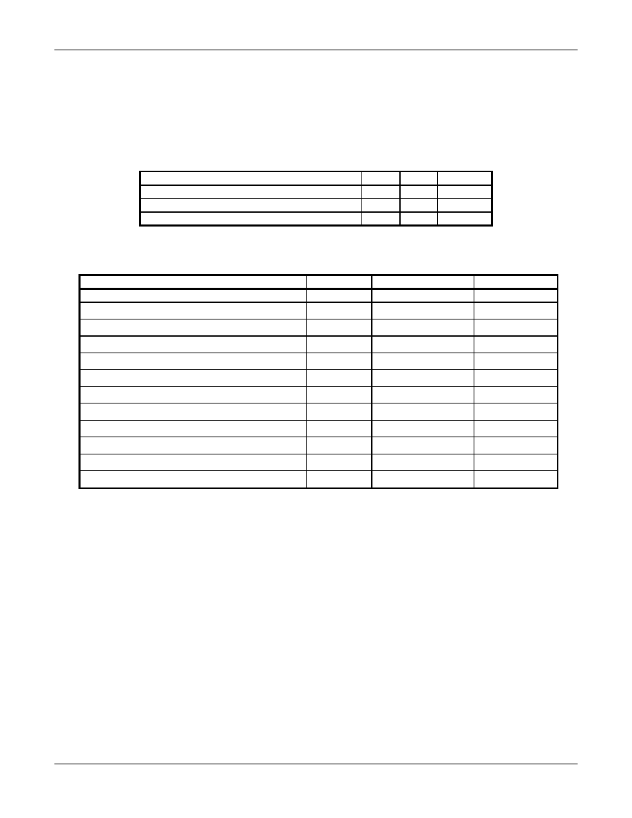
ELECTRICAL AND ENVIRONMENTAL SPECIFICATIONS
Operating Conditions and Absolute Maximum Ratings
Operating conditions are stated in Table 4.
The absolute maximum ratings are listed in Table 5.
Table 4. Operating Conditions
Parameter
Min.
Max.
Units
VDD
+3.0
+3.6
VDC
VGG
+4.75
+5.25
VDC
Ambient Temperature (TA)
0
70
0
�
C
Table 5. Absolute Maximum Ratings
Parameter
Symbol
Limits
Units
Supply Voltage
VDD
-0.5 to +4.0
V
Input Voltage
V
IN
-0.5 to (VGG +0.5)
V
Operating Temperature Range
T
A
-0 to +70
�C
Storage Temperature Range
T
STG
-55 to +125
�C
Voltage Applied to Outputs in High Impedance (Off) State
V
HZ
-0.5 to (VGG + 0.5)
V
DC Input Clamp Current
I
IK
�20
mA
DC Output Clamp Current
I
OK
�20
mA
Static Discharge Voltage (25�C)
V
ESD
�2500
V
Latch-up Current (25�C)
I
TRIG
�300
mA
Latch-up Current (125�C)
I
TRIG
�150
mA
Latch-up Current (25�C)
I
TRIG
�400
mA
Maximum Junction Temperature
T
J
125
�C

AnyPortTM Multi-Service Access Processor
RL56CSMV/3 and RL56CSM/3
MD233
Conexant
11
Current and Power Requirements
The current and power requirements are listed in Table 6.
Table 6. Current and Power Requirements
DDP Clock at 28.224 MHz
DDP Clock at 45 MHz
Mode
Typ.
Current
(mA)
Max.
Current
(mA)
Typ.
Power
(mW)
Max.
Power
(mW)
Typ.
Current
(mA)
Max.
Current
(mA)
Typ.
Power
(mW)
Max.
Power
(mW)
RL56CSM/3 (R7138)
Normal mode
300
305
990
1100
NA
NA
NA
NA
Sleep mode
163
540
RL56CSMV/3 (R7178)
Normal mode
275
280
910
1010
330
333
1090
1200
Sleep mode
152
500
152
500
Notes:
1. Current and power figures represent entire device (3 channels).
2. Test Conditions: VDD = 3.3 VDC for typical values; VDD = 3.6 VDC for maximum values.
TA = 0�C to 70�C
3. f = internal operating frequency: MCU = 40 MHz; DDP = 28.224 MHz (during non-G.728 modes) or 45 MHz (during G.728 mode).
BGA Thermal Characteristics
The BGA thermal characteristics are listed in Table 7.
Table 7. Thermal Characteristics
Natural Convection Cooling
Forced Convection Cooling at 1 m/s
Die Name
Die Number
Tdiff (
�
�
�
�
C)
Trise
(
�
�
�
�
C)
Tmax
(
�
�
�
�
C)
Tcase
(
�
�
�
�
C)
Trise
(
�
�
�
�
C)
Tmax
(
�
�
�
�
C)
Tcase
(
�
�
�
�
C)
MCU
1
2.0
�
C
27
97
95
23
93
91
DDP
2, 3, and 4
2.0
�
C
22
92
90
17.5
87.5
85.5
Notes:
1. The thermal performance of multi die BGA packages is shown by temperature rise over the ambient temperature [
�
C] for different devices
inside the package. The maximum operating junction temperature and case temperature can be estimated as follows:
Where:
Tambient = Ambient temperature (specified at 70
�
C) measured 2 inches above the center of the package.
Tdiff = Temperature difference between junction and case (specified for a given die).
Trise = Temperature rise (specified for a given die for Natural Convection and Forced Convection at 1 m/s conditions).
Tmax = Maximum operating junction temperature = Tambient + Trise [
�
C].
Tcase = Case temperature = Tmax - Tdiff.[
�
C].
Example: Hottest Die; natural convection case with maximum Tambient = 70
�
C:
Tdiff = 2.0
�
C (the case temperature for the hottest die is ~2.0
�
C lower than the maximum junction temperature).
Tmax = Tambient + Trise [
�
C] = 70 +27 = 97
�
C.
Tcase = Tmax � Tdiff [
�
C] = 97 - 2.0 = 95
�
C.
2. Maximum allowable junction temperature = 125
�
C.

RL56CSMV/3 and RL56CSM/3
AnyPortTM Multi-Service Access Processor
12
Conexant
MD233
Package Dimensions - 340-Pin BGA

AnyPortTM Multi-Service Access Processor
RL56CSMV/3 and RL56CSM/3
MD233
Conexant
13
REFERENCE
Table 8 identifies referenced specifications and recommendations.
Table 8. Referenced Specifications/Recommendations
Reference Number
Description
International Telecommunication Union (ITU) Recommendations
G.168
Digital network echo cancellers
G.711
Pulse code modulation (PCM) of voice frequencies
G.723.1
Dual rate speech coder for multimedia communications transmitting at 5.3 and 6.3 kbit/s
G.723.1 Annex A
Silence compression scheme
G.723.1 Annex B
Alternative specification based on floating point arithmetic
G.726
40, 32, 24, 16 kbit/s adaptive differential pulse code modulation (ADPCM)
G.727
5-, 4-, 3- and 2-bits/sample embedded adaptive differential pulse code modulation (ADPCM)
G.728
Coding of speech at 16 kbit/s using low-delay code excited linear prediction
G.729
Coding of speech at 8 kbit/s using conjugate structure algebraic-code-excited linear-prediction (CS-ACELP)
G.729 Annex A
Reduced complexity 8 kbit/s CS-ACELP speech codec
G.729 Annex B
A silence compression scheme for G.729 optimized for terminals conforming to Recommendation V.70
Q.24
DTMF Detection
V.110
Support of data terminal equipments with V-series type interfaces by an integrated services digital network
V.120
Support by an ISDN of data terminal equipment with V-series type interfaces with provision for statistical
multiplexing
V.17
A 2-wire modem for facsimile applications with rates up to 14 400 bit/s
V.21
300 bits per second duplex modem standardized for use in the general switched telephone network
V.22
1200 bits per second duplex modem standardized for use in the general switched telephone network and on
point-to-point 2-wire leased telephone-type circuits
V.22 bis
2400 bits per second duplex modem using the frequency division technique standardized for use on the general
switched telephone network and on point-to-point 2-wire leased telephone-type circuits
V.23
600/1200-baud modem standardized for use in the general switched telephone network
V.27 ter
4800/2400 bits per second modem standardized for use in the general switched telephone network
V.29
9600 bits per second modem standardized for use on point-to-point 4-wire leased telephone-type circuits
V.32
A family of 2-wire, duplex modems operating at data signalling rates of up to 9600 bit/s for use on the general
switched telephone network and on leased telephone-type circuits
V.32 bis
A duplex modem operating at data signalling rates of up to 14 400 bit/s for use on the general switched
telephone network and on leased point-to-point 2-wire telephone-type circuits
V.33
14 400 bits per second modem standardized for use on point-to-point 4-wire leased telephone-type circuits
V.34
A modem operating at data signalling rates of up to 33 600 bit/s for use on the general switched telephone
network and on leased point-to-point 2-wire telephone-type circuits
V.90
A digital modem and analogue modem pair for use on the public switched telephone network (PSTN) at data
signalling rates of up to 56000 bits/sec downstream and up to 33600 bits/s upstream
European Telecommunications Standards Institute (ETSI)
ETSI SMG GSM 06.10
Full Rate voice codec.
Internet Engineering Task Force (IETF)
ietf-avt-rtp-new-00.txt
IETF, December 5, 1997
RTP: A Transport Protocol for Real-Time Applications

Further Information
literature@conexant.com
1-800-854-8099 (North America)
33-14-906-3980 (International)
Web Site
www.conexant.com
World Headquarters
Conexant Systems, Inc.
4311 Jamboree Road
P. O. Box C
Newport Beach, CA
92658-8902
Phone: (949) 483-4600
Fax: (949) 483-6375
U.S. Florida/South America
Phone: (727) 799-8406
Fax: (727) 799-8306
U.S. Los Angeles
Phone: (805) 376-0559
Fax: (805) 376-8180
U.S. Mid-Atlantic
Phone: (215) 244-6784
Fax: (215) 244-9292
U.S. North Central
Phone: (630) 773-3454
Fax: (630) 773-3907
U.S. Northeast
Phone: (978) 692-7660
Fax: (978) 692-8185
U.S. Northwest/Pacific West
Phone: (408) 249-9696
Fax: (408) 249-7113
U.S. South Central
Phone: (972) 733-0723
Fax: (972) 407-0639
U.S. Southeast
Phone: (919) 858-9110
Fax: (919) 858-8669
U.S. Southwest
Phone: (949) 483-9119
Fax: (949) 483-9090
APAC Headquarters
Conexant Systems Singapore,
Pte. Ltd.
1 Kim Seng Promenade
Great World City
#09-01 East Tower
SINGAPORE 237994
Phone: (65) 737 7355
Fax: (65) 737 9077
Australia
Phone: (61 2) 9869 4088
Fax: (61 2) 9869 4077
China
Phone: (86 2) 6361 2515
Fax: (86 2) 6361 2516
Hong Kong
Phone: (852) 2827 0181
Fax: (852) 2827 6488
India
Phone: (91 11) 692 4780
Fax: (91 11) 692 4712
Korea
Phone: (82 2) 565 2880
Fax: (82 2) 565 1440
Phone: (82 53) 745 2880
Fax: (82 53) 745 1440
Europe Headquarters
Conexant Systems France
Les Taissounieres B1
1681 Route des Dolines
BP 283
06905 Sophia Antipolis Cedex
FRANCE
Phone: (33 4) 93 00 33 35
Fax: (33 4) 93 00 33 03
Europe Central
Phone: (49 89) 829 1320
Fax: (49 89) 834 2734
Europe Mediterranean
Phone: (39 02) 9317 9911
Fax: (39 02) 9317 9913
Europe North
Phone: (44 1344) 486 444
Fax: (44 1344) 486 555
Europe South
Phone: (33 1) 41 44 36 50
Fax: (33 1) 41 44 36 90
Middle East Headquarters
Conexant Systems
Commercial (Israel) Ltd.
P. O. Box 12660
Herzlia 46733, ISRAEL
Phone: (972 9) 952 4064
Fax: (972 9) 951 3924
Japan Headquarters
Conexant Systems Japan Co., Ltd.
Shimomoto Building
1-46-3 Hatsudai,
Shibuya-ku, Tokyo
151-0061 JAPAN
Phone: (81 3) 5371-1567
Fax: (81 3) 5371-1501
Taiwan Headquarters
Conexant Systems, Taiwan Co., Ltd.
Room 2808
International Trade Building
333 Keelung Road, Section 1
Taipei 110, TAIWAN, ROC
Phone: (886 2) 2720 0282
Fax: (886 2) 2757 6760
SO990326(V1.2)