 | –≠–ª–µ–∫—Ç—Ä–æ–Ω–Ω—ã–π –∫–æ–º–ø–æ–Ω–µ–Ω—Ç: RM912 | –°–∫–∞—á–∞—Ç—å:  PDF PDF  ZIP ZIP |

Data Sheet
100635G
2000, Conexant Systems, Inc. All Rights Reserved.
August 2000
RM912
CDMA/AMPS 3≠4 Volt Power Amplifier (824≠849 MHz)
The RM912 dual mode Code Division Multiple Access (CDMA)/Advanced Mobile
Phone Service (AMPS) Power Amplifier is a fully matched 6-pin LCC surface mount
module designed for mobile units operating in the 824-849 MHz cellular bandwidth.
This device meets stringent IS95 CDMA linearity requirements to beyond 28 dBm
output power and can be driven to power output levels beyond 31 dBm for high
efficiency FM mode operation. A single GaAs Microwave Monolithic Intergrated
Circuit (MMIC) contains all active circuitry in the module. The MMIC contains
on-board bias circuitry, as well as input and interstage matching circuits. The output
match is realized off-chip within the module package to optimize efficiency and power
performance into a 50
load. This device is manufactured with Conexant's GaAs HBT
process that provides for all positive voltage DC supply operation while maintaining
high efficiency and good linearity. Primary bias to the RM912 can be supplied directly
from a three cell nickel-cadmium, single cell lithium-ion, or other suitable battery with
output in the 3-4 volt range. Power down is accomplished by setting the voltage on
the low current reference pin to zero volts. No external supply side switch is needed
as typical "off" leakage is a few microamperes with full primary voltage supplied from
the battery.
Functional Block Diagram
MMIC
MODULE
RF
Input
RF
Output
VCC1
GND
GND
VCC2
VREF
Driver
Stage Bias
Power
Stage Bias
Input
Match
DA
Inter
Stage
Match
PA
Output
Match
(6, 7)
(3)
(2)
(5)
(1)
(4)
(6, 7)
Distinguishing Features
∑
Low voltage positive bias supply
∑
Good linearity
∑
High efficiency
∑
Dual mode operation
∑
Large dynamic range
∑
6-pin LCC package
(6 x 6 x 1.5 mm)
∑
Power down control
Applications
∑
Digital cellular (CDMA)
∑
Analog cellular (AMPS)
∑
Wireless local loop

Electrical Specifications
RM912
CDMA/AMPS 3≠4 Volt Power Amplifier (824≠849 MHz)
2
Conexant
100635G
Electrical Specifications
The following tables list the electrical characteristics of the RM912 Power Amplifier.
Table 1
lists
the absolute maximum rating for continuous operation.
Table 2
lists the recommended operating
conditions for achieving the electrical performance listed in
Table 3
.
Table 3
lists the electrical
performance of the RM912 Power Amplifier over the recommended operating conditions.
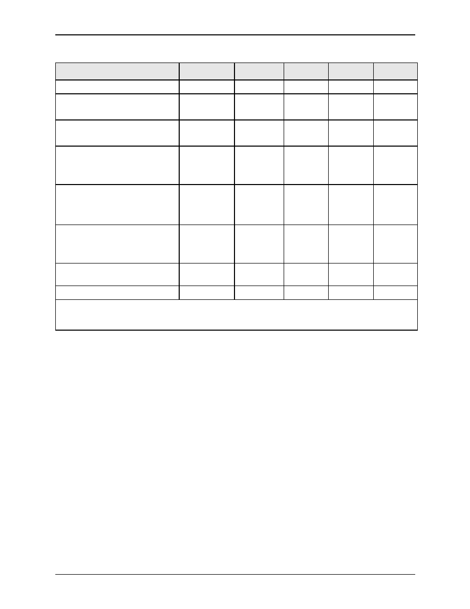
Table 1. Absolute Maximum Ratings
(1)
Parameter
Symbol
Min
Nominal
Max
Unit
RF Input Power
Pin
--
3.0
6.0
dBm
Supply Voltage
Vcc
--
3.4
5.0
Volts
Reference Voltage
Vref
--
3.0
3.3
Volts
Case Operating Temperature
Tc
≠30
25
+110
∞C
Storage Temperature
Tstg
≠55
--
+125
∞C
NOTE(S):
(1)
No damage assuming only one parameter is set at limit at a time with all other parameters set at or below nominal value.
Table 2. Recommended Operating Conditions
Parameter
Symbol
Min
Nominal
Max
Unit
Supply Voltage
Vcc
3.2
3.4
4.2
Volts
Reference Voltage
Vref
2.9
3.0
3.1
Volts
Operating Frequency
Fo
824.0
836.5
849.0
MHz
Operating Temperature
To
≠30
+25
+85
∞C

RM912
Electrical Specifications
CDMA/AMPS 3≠4 Volt Power Amplifier (824≠849 MHz)
100635G
Conexant
3
Table 3. Electrical Specifications for CDMA / AMPS Nominal Operating Conditions
(1)
Characteristics
Condition
Symbol
Min
Typical
Max
Unit
Quiescent current
Vref = 3.0
Vref = 2.9
Iq
Iq
--
--
100.0
80.0
--
--
mA
mA
Gain≠Digital
Po = 0 dBm
Po = 28 dBm
G
G
p
26.0
27.0
28.0
29.0
--
--
dB
dB
Gain≠Analog
Po = 0 dBm
Po = 31 dBm
G
Gp
26.0
26.0
28.0
28.0
--
--
dB
dB
Power Added Efficiency
≠ Analog Mode
≠ Digital Mode
Po = 31 dBm
Po = 28 dBm
PAEa
PAEd
43.0
32.0
45.0
34.0
--
--
%
%
Adjacent Channel Power
(2)
≠ 885 kHz Offset
≠1980 kHz Offset
Po
28 dBm
Po
28 dBm
ACP1
ACP2
--
--
≠50.0
≠58.0
≠48.0
≠56.0
dBc
dBc
Harmonic Suppression
≠ Second
≠ Third
Po
31 dBm
Po
31 dBm
AFo2
AFo3
--
--
≠42.0
≠45.0
≠30.0
≠30.0
dBc
dBc
Noise Power in RX Band
869-894 MHz
Po @ 28 dBm
RxBN
--
≠134.0
≠133.0
dBm/Hz
Noise Figure
--
NF
--
6.0
--
dB
Input Voltage Standing Wave
Ratio
--
VSWR
--
1.4:1
--
--
Stability (Spurious output)
5:1 VSWR
All phases
S
--
--
≠60.0
dBc
Ruggedness ≠ No damage
Po
31 dBm
Ru
10:1
--
--
VSWR
NOTE(S):
(1)
Vcc = +3.4 V, Vref = +3.0 V, Freq = 836.5 MHz, Tc = 25 ∞C, unless otherwise specified.
(2)
ACP is specified per IS95 as the ratio of the total in-band power (1.23 MHz BW) to adjacent power in a 30 kHz BW.
Electrical Specifications
RM912
CDMA/AMPS 3≠4 Volt Power Amplifier (824≠849 MHz)
4
Conexant
100635G
Table 4. Electrical Specifications Limits for CDMA / AMPS Recommended Operating Conditions
(1)
Characteristics
Condition
Symbol
Min
Max
Unit
Quiescent current
Vref = 3.0
Iq
--
140.0
mA
Gain≠Digital
Po = 0 dBm
Po = 28 dBm
G
G
p
25.0
25.0
29.0
32.0
dB
dB
Gain≠Analog
Po = 0 dBm
Po = 31dBm
G
Gp
25.0
24.0
29.0
32.0
dB
dB
Power Added Efficiency
≠ Analog Mode
≠ Digital Mode
Po = 31 dBm
Po = 28 dBm
PAEa
PAEd
42.0
32.0
--
--
%
%
Adjacent Channel Power
(2)
≠ 885 kHz Offset
≠1980 kHz Offset
Po
28 dBm
Po
28 dBm
ACP1
ACP2
--
--
≠44.0
≠56.0
dBc
dBc
Harmonic Suppression
≠ Second
≠ Third
Po
31 dBm
Po
31 dBm
AFo2
AFo3
--
--
≠40.0
≠40.0
dBc
dBc
Noise Power in RX Band
869--894 MHz
Po @ 28 dBm
RxBN
--
≠131.0
dBm/Hz
Input Voltage Standing Wave Ratio
--
VSWR
--
2:1
--
NOTE(S):
(1)
Per
Table 2
.
(2)
ACP is specified per IS95 as the ratio of the total in-band power (1.23 MHz BW) to adjacent power in a 30 kHz BW.
RM912
Characterization Data
CDMA/AMPS 3≠4 Volt Power Amplifier (824≠849 MHz)
100635G
Conexant
5
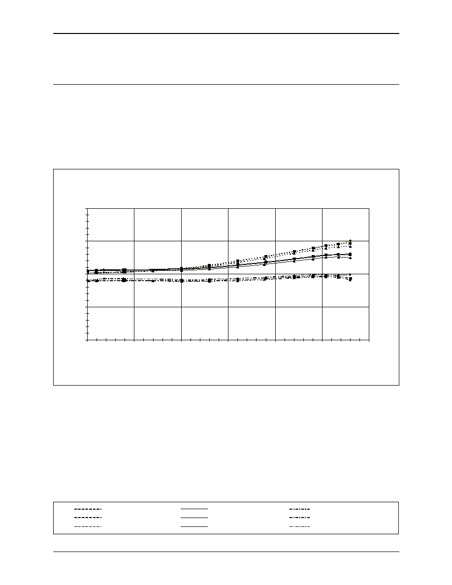
Characterization Data
The following charts illustrate the characteristics of a typical RM912 Power Amplifier tested in the
evaluation board described in the following section. The amplifier was selected by characterizing a
group of devices and choosing a part with average electrical performance at both nominal and
worst case (limit) conditions.
Figures 1
through
4
illustrate the digital signal characteristics and
Figures 5
through
8
illustrate the analog characteristics of the RM912.
Legend
Figure 1. Digital Gain vs. Output Power
22.50
25.00
27.50
30.00
32.50
0.00
5.00
10.00
15.00
20.00
25.00
30.00
Output Power (dB m)
Ga
in (
d
B
)
Vref = 3.0V, Vcc = 3.4V
N
824 MHz @ ≠30
∞C
N
824 MHz @ +25
∞C
N
824 MHz @ +85
∞C
I
837 MHz @ ≠30
∞C
I
837 MHz @ +25
∞C
I
837 MHz @ +85
∞C
L
849 MHz @ ≠30
∞C
L
849 MHz @ +25
∞C
L
849 MHz @ +85
∞C