
THE CONNOR-WINFIELD CORP.
2111 COMPREHENSIVE DRIVE.
AURORA, IL 60505.
FAX (630) 851-5040.
PHONE (630) 851-4722.
WWW.CONWIN.COM
P R O D U C T D A T A S H E E T
Specifications subject to change without notice.
DATA SHEET #:
REV:
DATE:
PAGE
OF
Copyright 2001 Connor-Winfield all rights reserved.
a
CRYSTAL CONTROLLED OSCILLATORS
The Connor-Winfield
VPLD61J3EG5 is a 3.3V
Voltage Controlled Crystal
Oscillator (VCXO) with
Differential LVPECL outputs
and Enable/Disable function.
The VPLD61J3EG5 is
designed for use with PLL
systems in SONET/SDH
systems requiring low jitter
and tight frequency stability
over the industrial
temperature range. No
multiplication schemes are
used in this oscillator design.
1
2
VPLD61J3EG5 - 155.52MHz
VCXO
SERIES
CENTER
FREQUENCY
FEATURES
DESCRIPTION
ORDERING INFORMATION
SURFACE MOUNT PACKAGE
3.3V OPERATION
LOW JITTER <1pS RMS
FREQUENCY STABILITY: ±20ppm
TEMPERATURE RANGE: -40 to 85∞C
DIFFERENTIAL LVPECL OUTPUTS
ENABLE / DISABLE FUNCTION
RoHS 5/6 COMPLIANT
3.3V SURFACE MOUNT VCXO OSCILLATOR
VPLD61J3EG5
Vx567
00
08/10/06
CW 0632
VPLD61J3EG5
155.52M
ABSOLU TE MAX IMUM R ATINGS
TABLE 1.0
PARAMETER
UNITS
MINIMUM
NOMINAL MAXIMUM
UNITS
NOTE
Storage Temperature
-40
-
85
∞C
Supply Voltage
(Vcc)
-0.5
-
7.0
Vdc
Control Voltage
(Vc)
-0.5
-
7.0
Vdc
OPERATING SPECIFIC ATIONS
TABLE 2.0
PARAMETER
MINIMUM
NOMINAL MAXIMUM
UNITS
NOTE
Center Frequency
(Fo)
16.384
-
200
MHz
Frequency Stability
-25
-
25
ppm
1
Operating Temperature Range
-40
-
85
∞C
Supply Voltage
(Vcc)
3.135
3.3
3.465
Vdc
Supply Current
(Icc)
-
-
100
mA
Jitter (BW=10Hz to 20MHz)
-
-
5
ps rms
Jitter (BW=12kHz to 80MHz)
-
-
1
ps rms
SSB Phase Noise at 10Hz offset
-
-50
-
dBc/Hz
SSB Phase Noise at 100Hz offset
-
-80
-
dBc/Hz
SSB Phase Noise at 1KHz offset
-
-110
-
dBc/Hz
SSB Phase Noise at 10KHz offset
-
-135
-
dBc/Hz
SSB Phase Noise at 100KHz offset
-
-140
-
dBc/Hz
Oscillator startup time
-
-
10
ms
INPUT CHARACTERISTICS
TABLE 3.0
PARAMETER
MINIMUM
NOMINAL
MAXIMUM
UNITS
NOTE
Control Voltage Range
(Vc)
0.3
1.65
3.0
Vdc
Absolute Pull Range (APR)
+/-50
-
-
ppm
2
Monotonic Linearity
-10
-
10
%
Input Impedance
-
50K
-
Ohm
Modulation Bandwidth (3dB)
10
-
-
KHz
Enable Input Voltage (Low)
(Vil)
-
-
1.68
Vdc
3
Disable Input Voltage (High)
(Vih)
2.275
-
-
Vdc
3
LVPECL OUTPUT CHARACTERISTICS
TABLE 4.0
PARAMETER
MINIMUM
NOMINAL
MAXIMUM
UNITS
NOTE
LOAD
-
-
50
Ohms
4
Voltage (High)
(Voh)
2.275
-
-
Vdc
(Low)
(Vol)
-
-
1.68
Vdc
Duty Cycle at 50% Level
45
50
55
%
Rise / Fall Time measured @ 20% to 80%
-
-
1.0
ns
PACKAG E CHARACTERISTICS
TABLE 5.0
Package
Non-hermetic package consisting of an FR4 substrate with grounded metal
cover.
PROCESS RECOMMENDATIONS
TABLE 6.0
Soldering Process
See the solder profile page 2.
Wash
Ultrasonic cleaning is not recommended.
Notes
1.0
Inclusive of calibration @ 25∞C, frequency stability vs. temperature, control voltage (Vc) = 1.65 Vdc.
2.0
Absolute pull range (APR) is the minimum guaranteed pull range of the VCXO under all conditions over lifetime
operation including aging for ten years. The APR is referenced to Fo.
3.0
When oscillator is disabled the true output is in a low state (Vol) and the complementary output is in the high
state (VoH)
4.0
50 ohm termination into Vcc-2V or Thevein equivalent.
THE CONNOR-WINFIELD CORP.
2111 COMPREHENSIVE DRIVE.
AURORA, IL 60505.
FAX (630) 851-5040.
PHONE (630) 851-4722.
WWW.CONWIN.COM
P R O D U C T D A T A S H E E T
Specifications subject to change without notice.
DATA SHEET #:
REV:
DATE:
PAGE
OF
Copyright 2001 Connor-Winfield all rights reserved.
a
CRYSTAL CONTROLLED OSCILLATORS
2
2
Vx567
00
08/10/06
1.65V
E/D
2
Dimensional Tolerance:
±.005 (.127mm)
V
P
L
D
6
1
J
3
E
G
5
1
5
5
.
5
2
M
C
W
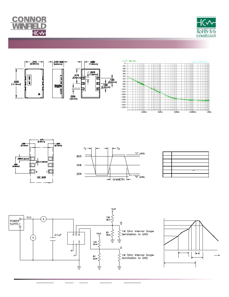
Pin
Function
1
Control Voltage
2
Enable / Disable
3
Ground (Case)
4
Output Q
5
Comp Output Q
6
Vcc
Typical Phase Noise for VPLD61J3EG5
Package Outline
100
∞C
150
∞C
225
∞C
25∞C
183∞C
360 Sec. Max.
60-120s
Max.
60-150s Max.
Time
Temperature
225∞C
0
tp
Ramp-Down Rate
6∞C/second max.
10-30s
Ramp-Up Rate
3∞C/second max.
from 150∞C to 225∞C.
Suggested Pad Layout
Output Waveform
Pin Connections
Test Circuit
Solder Profile