Specifications subject to change without notice. All dimensions in inches. © Copyright 1998 The Connor-Winfield Corporation
2111 Comprehensive Drive
Aurora, Illinois 60505
Phone: 630- 851- 4722
Fax: 630- 851- 5040
www.conwin.com
3.3V 5.0mm x 7mm
Surface Mount
High Frequency Oscillator
V751
VCXO
The Connor-Winfield, RoHS compliant, V751 is a
3.3V Voltage Controlled Crystal Oscillator (VCXO)
with LVPECL Differential outputs and enable/disable
function. The V751 is designed for use with applica-
tions utilizing a PLL system requiring low jitter and
tight frequency stability. No multiplication schemes
are used in this oscillator design. The surface mount
package is designed for high-density mounting and
is optimum for mass production.
Operating Specifications
Parameter
Minimum
Nominal
Maximum
Units
Notes
Center Frequency (Fo)
65
-
700
MHz
Operating Temperature Range
-40
-
70
∞C
Supply Voltage (Vcc)
3.135
3.3
3.465
Vdc
Supply Current (Icc)
-
-
100
mA
Jitter:
(BW=10Hz to 20 MHz)
-
-
15
ps RMS
(BW=12kHz to 20 MHz)
-
-
1.5
SSB Phase Noise at 10Hz offset
-
-65
-
at 100Hz offset
-
-95
-
at 1kHz offset
-
-125
-
dBc/Hz
at 10kHz offset
-
-140
-
at 100kHz offset
-
-145
-
Absolute Maximum Ratings
Parameter
Minimum
Nominal
Maximum
Units
Notes
Storage Temperature
-40
-
85
∞C
Supply Voltage (Vcc)
-0.5
-
7.0
Vdc
Control Voltage (Vc)
-0.5
-
Vcc+0.5
Vdc
Features:
RoHS Compliant
65 to 200MHz
3.3V Operation
Low Jitter <1pS RMS
Absolute Pull Range (APR): ±30ppm
Temperature Range: -40∞ to 85∞C
Differential LVPECL Outputs
Enable / Disable Function
Surface Mount Package
Tape and Reel Packaging
Notes:
1. Absolute pull range (APR) is the minimum guaranteed pull range of the VCXO under all conditions over the lifetime operation. Including calibration @ 25∞C,
frequency vs. change in temperature, frequency vs. change in supply voltage, frequency vs. change in load, shock and vibration and aging for ten years.
The APR is referenced to Fo. Positive Transfer Function.
2. Outputs are enabled with no connection on pad 2. When oscillator is disabled both outputs are in a high impedance state.
3. 50 ohm termination into Vcc-2V or Thevein equivalent.
Specifications subject to change without notice. All dimensions in inches. © Copyright 1998 The Connor-Winfield Corporation
Bulletin
Vx532
Page
1 of 2
Revision
00
Date
16 Dec 2004
US Headquarters:
630-851-4722
European Headquarters:
+353-61-472221
Input Characteristics
Parameter
Minimum
Nominal
Maximum
Units
Notes
Control Voltage Range (Vc)
0.3
1.65
3.0
Vdc
Absolute Pull Range (APR)
±30
-
-
ppm
1
Monotonic Linearity
-10
-
10
%
Input Impedance
-
60K
-
Ohm
Modulation Bandwidth (3dB)
25
-
-
kHz
Enable Input Voltage - Low (Vil)
-
-
1.68
Vdc
2
Disable Input Voltage - High (Vih) 2.275
-
-
LVPECL Output Characteristics
Parameter
Minimum
Nominal
Maximum
Units
Notes
Load
-
-
50
Ohms
3
Voltage High (Voh)
2.275
-
-
Vdc
Low (Vol)
-
-
1.68
Duty Cycle at 50% Level
45
50
55
%
Rise / Fall Time 20% to 80%
-
0.6
1.5
nS
Package Characteristics
Package
Hermetically sealed, ceramic package with grounded metal cover.
Specifications subject to change without notice. All dimensions in inches. © Copyright 1998 The Connor-Winfield Corporation
2111 Comprehensive Drive
Aurora, Illinois 60505
Phone: 630- 851- 4722
Fax: 630- 851- 5040
www.conwin.com
Bulletin
Vx532
Page
2 of 2
Revision
00
Date
16 Dec 2004
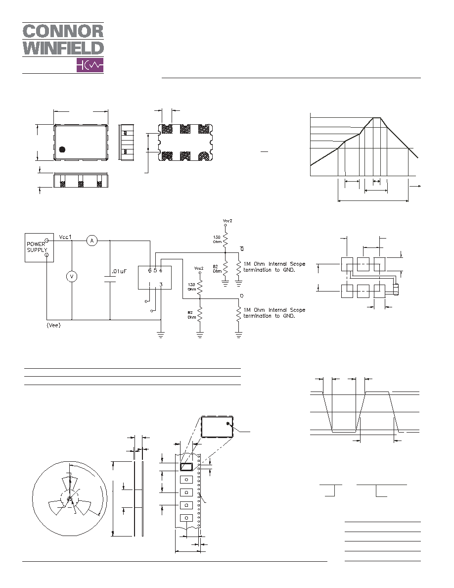
Suggested Pad Layout
Output Waveform
SYMMETRY
"0" LEVEL
"1" LEVEL
TR
TF
20%
50%
80%
Ordering Information
Bypass capacitor, C≠by, should be
ceramic capacitor
.01uf.
0.165
(4.2mm)
VDD
GROUND
C≠by
0.200
(5.08mm)
0.100
(2.54mm)
0.079
(2.0mm)
0.070
(1.8mm)
7.48 DIA
(190mm)
.69
(17.5mm)
.315
(8.0mm)
.039 R
(1.0mm)
.826 DIA
(21mm)
.511 DIA
(13mm)
9.84 DIA
(250mm)
MEETS EIA--481A and EIAJ--1009B
2,000 PCS/REEL
120
.08
(2.0mm)
3.15
(8.0mm)
.08
(2.0mm)
.157
(4.0mm)
.06 DIA
(1.5mm)
.31
(7.9mm)
.21
(5.4mm)
PIN 1
.295
(7.5mm)
.07
(1.75mm)
.63
(16.0mm)
V751 - 77.76 MHz
VCXO
SERIES
CENTER
FREQUENCY
CW V751
77.76M
0428
.275 MAX
(7.0mm)
.070 MAX
(1.8mm)
0.102
(2.6mm)
.197 MAX
(5.0mm)
0.055
(1.4mm)
Dimensional ±.02" (±0.5mm)
Tolerance: ±.008"
(±0.2mm)
#1
#2
#3
#6
#5
#4
#1
#2
#3
#6
#5
#4
Dimensions
1.65V
E/D
2
Output Enable Function
Enable / Disable Function (Pad 2)
Output
Low
Enable
High
Disable (High Inpedance)
Pin Function
1: Control Voltage
2: Enable / Disable
3: Ground (Case)
4: Output Q
5: Output Q
6: Vcc
Solder Profile
0
360 Sec. Max.
120 S
Max.
10 S
60 S
Max.
Time
Temperature
260∞C
260∞C
220∞C
180∞C
150∞C
120∞C
Tape and Reel Dimensions
Test Circuit