MODEL
LCC30A-1
LCC30A-2
LCC30A-3
LCC30A-4
DC OUTPUT
V1
5V 3.0(Peak 4.5)A
5V 3.0(Peak 4.5)A
5V 3.0(Peak 4.5)A
3.3V 4.0(Peak 6.0)A
V2
12V 1.2(Peak 2.0)A
15V 1.0(Peak 2.0)A
24V 0.5(Peak 1.3)A
12V 1.2(Peak 2.0)A
V3
*
1
12V 0.3(Peak 0.45)A
15V 0.3(Peak 0.45)A
5V 0.5(Peak 0.75)A
5V 0.5(Peak 0.75)A
SPECIFICATIONS
MODEL
LCC30A-1
LCC30A-2
LCC30A-3
LCC30A-4
INPUT
VOLTAGE[V]
AC85 - 132 1
f
or DC110 - 170
CURRENT[A]
ACIN 100V 0.8typ (Io=100%)
FREQUENCY[Hz]
47 - 440 or DC
EFFICIENCY[%]
ACIN 100V 72typ (Io=100%)
67typ (Io=100%)
INRUSH CURRENT[A] ACIN 100V 25typ (Io=100%) (At cold start)
LEAKAGE CURRENT[mA]
0.5 max (60Hz, by UL and DEN-AN)
OUTPUT
VOLTAGE[V]
5
12
12
5
15
15
5
24
5
3.3
12
5
CURRENT[A]
*
2
0 - 3.0(Peak 4.5) 0 - 1.2(Peak 2.0) 0 - 0.3(Peak 0.45) 0 - 3.0(Peak 4.5) 0 - 1.0(Peak 2.0) 0 - 0.3(Peak 0.45) 0 - 3.0(Peak 4.5) 0 - 0.5(Peak 1.3) 0 - 0.5(Peak 0.75) 0 - 4.0(Peak 6.0) 0 - 1.2(Peak 2.0) 0 - 0.5(Peak 0.75)
LINE REGULATION[mV]
20max
48max
48max
20max
60max
60max
20max
100max 20max
20max
48max
20max
LOAD REGULATION[mV]
100max 120max 150max 100max 120max 150max 100max 150max 100max 40max
120max 100max
RIPPLE[mVp-p]
0 to +50
C
*
3
100max 120max 120max 100max 120max 120max 100max 120max 120max 80max
120max 120max
-10 - 0
C
*
3
150max 160max 160max 150max 160max 160max 150max 160max 160max 140max 160max 160max
RIPPLE NOISE[mVp-p]
0 to +50
C
*
3
120max 150max 150max 120max 150max 150max 120max 150max 150max 120max 150max 150max
-10 - 0
C
*
3
170max 180max 180max 170max 180max 180max 170max 180max 180max 160max 180max 180max
TEMPERATURE REGULATION[mV]
0 to +50
C
50max
350max 350max 50max
350max 350max 50max
480max 350max 50max
350max 350max
-10 to +50
C
60max
420max 420max 60max
420max 420max 60max
580max 420max 60max
420max 420max
DRIFT[mV]
*
4
20max
xx
xx
20max
xx
xx
20max
xx
xx
20max
xx
xx
START-UP TIME[ms]
100max (ACIN 85V, Io=100%)
HOLD-UP TIME[ms]
10typ (ACIN 85V, Io=100%) , 20typ (ACIN 100V, Io=100%)
OUTPUT VOLTAGE ADJUSTMENT RANGE[V]
*
5
Fixed
Fixed
Fixed
Fixed
Fixed
Fixed
Fixed
Fixed
Fixed
3.00 - 3.60 Fixed
Fixed
OUTPUT VOLTAGE SETTING[V]
4.9 to 5.3 11.4 to 12.6 11.4 to 12.6 4.9 to 5.3 14.25 to 15.75 14.25 to 15.75 4.9 to 5.3 22.8 to 25.2 4.75 to 5.25
xx
11.4 to 12.6 4.75 to 5.25
PROTECTION
CIRCUIT AND
OTHERS
OVERCURRENT PROTECTION Works over 105% of rating and recovers automatically
OVERVOLTAGE PROTECTION
Works at 115 - 140% of rating (V1 only)
OPERATING INDICATION
Not provided
REMOTE SENSING
Not provided
REMOTE ON/OFF
Not provided
ISOLATION
INPUT-OUTPUT
AC2,000V 1minute, Cutoff current = 10mA, DC500V 50M
W
min (At Room Temperature)
INPUT-FG
AC2,000V 1minute, Cutoff current = 10mA, DC500V 50M
W
min (At Room Temperature)
OUTPUT-FG
AC500V 1minute, Cutoff current = 100mA, DC500V 50M
W
min (At Room Temperature)
OUTPUT-OUTPUT(V1,V2,V3) AC100V 1minute, Cutoff current = 100mA, DC100V 10M
W
min (At Room Temperature)
ENVIRONMENT
OPERATING TEMP.,HUMID.AND ALTITUDE -10 to +60
C
, 20 - 90%RH (Non condensing), 3,000m (10,000feet)
STORAGE TEMP.,HUMID.AND ALTITUDE -20 to +75
C
, 20 - 90%RH (Non condensing), 9,000m (30,000feet)
VIBRATION
10 - 55Hz, 19.6m/s
2
(2G), 3minutes period, 60minutes each along X, Y and Z axis
IMPACT
196.1m/s
2
(20G), 11ms, once each X, Y and Z axis
SAFETY AND
NOISE
REGULATIONS
AGENCY APPROVALS
UL60950-1, C-UL Complies with DEN-AN (At only AC input)
CONDUCTED NOISE
Complies with FCC-B, VCCI-B
OTHERS
CASE SIZE/WEIGHT
COOLING METHOD
Convection
65
X
26
X
120mm (W
X
H
X
D) / 170g max
*
1
Because V2 - V3 is isolated,V3 can be as used -VOUT.
*
2
Peak load for 10sec. or less is acceptable if the peak total wattage is less than the rated
wattage(-1: 33W, -2: 34.5W, -3: 34.5W, -4: 34.5W).When the load of V1 is 0A, other output
can be drawn by 80% of rated current.
*
3
Measured by 20MHz oscilloscope or Ripple-Noise meter (equivalent to KEISOKU-
GIKEN:RM101).
*
4
Drift is the change in DC output for an eight hour period after a half-hour warm-up at 25
C
with the input voltage held constant at the rated input/output.
*
5
Adjustment of output voltage for V1 (+5V+5%) is possible (Optional).
Please refer to 2.5 minimum output current and 4.2 derating.
*
Avoid prolonged use under over-load.
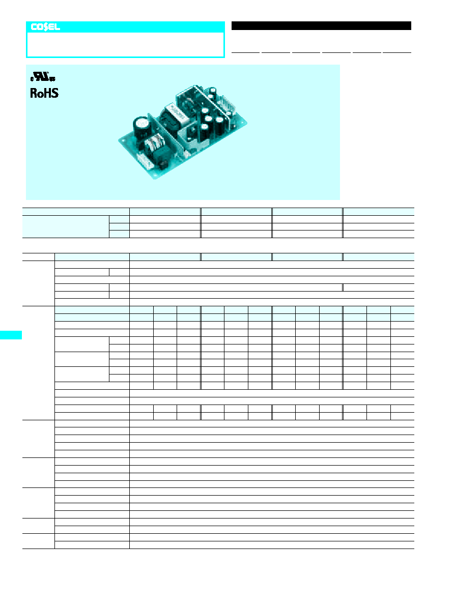
LCC30A
Rugged PCB type
LC
C
30
A
-1
-
O
Ordering information
1
Series name
2
Multiple output
3
Output wattage
4
100/120V input
5
Output voltage combina-
tion
6
Optional
A :G2 - V3 Common
C :with Coating
G :Low leakage current
Y :with Potentiometer
R
1
2
3
4
5
6
LCC
F-30