 | –≠–ª–µ–∫—Ç—Ä–æ–Ω–Ω—ã–π –∫–æ–º–ø–æ–Ω–µ–Ω—Ç: ZS34812 | –°–∫–∞—á–∞—Ç—å:  PDF PDF  ZIP ZIP |

MODEL
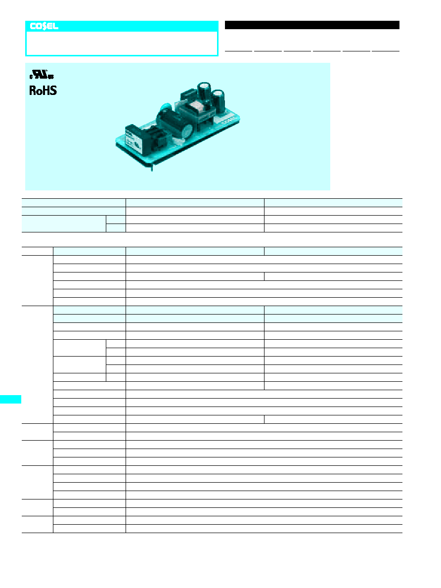
VAA505
VAA512
MAX OUTPUT WATTAGE[W]
5.0
5.4
DC OUTPUT
VOLTAGE[V] 5
12
CURRENT[A] 1.0
0.45
SPECIFICATIONS
MODEL
VAA505
VAA512
INPUT
VOLTAGE[V]
AC85 - 132 1
f
or DC110 - 170
CURRENT[A]
*
1
0.13typ (ACIN 100V, Io=100%)
EFFICIENCY[%]
*
1
75typ
77typ
FREQUENCY[Hz]
47 - 440 or DC
INRUSH CURRENT[A]
*
1
15typ (ACIN 100V, Io=100%)
LEAKAGE CURRENT[mA] 0.5max (60Hz According to UL and DEN-AN)
OUTPUT
VOLTAGE[V]
5
12
CURRENT[A]
1.0
0.45
LINE REGULATION[mV]
20max
48max
LOAD REGULATION[mV] 40max
100max
RIPPLE[mVp-p]
0 to +55
C
*
2
80max
120max
-10 - 0
C
*
2
140max
160max
RIPPLE NOISE[mVp-p]
0 to +55
C
*
2
120max
150max
-10 - 0
C
*
2
160max
180max
TEMPERATURE COEFFICIENT[mV] -10 to +55
C
50max
120max
DRIFT[mV]
*
3
20max
48max
OUTPUT VOLTAGE ADJUSTMENT RANGE Fixed
START-UP TIME[ms]
200max (ACIN 85V, Io=100%)
HOLD-UP TIME[ms]
10typ (ACIN 85V, Io=100%), 20typ (ACIN 100V, Io=100%)
OUTPUT VOLTAGE SETTING[V]
*
1
4.90 - 5.30
11.40 - 12.60
PROTECTION
CIRCUIT
OVERCURRENT PROTECTION Works over 105% of rating and recovers automatically
OVERVOLTAGE PROTECTION
Works over 115% of rating (by zener diode clamping)
ISOLATION
INPUT-OUTPUT
AC2,000V 1minute, Cutoff current = 10mA, DC500V 50M
W
min (At Room Temperature)
INPUT-FG
AC2,000V 1minute, Cutoff current = 10mA, DC500V 50M
W
min (At Room Temperature)
OUTPUT-FG
AC500V 1minute, Cutoff current = 100mA, DC500V 50M
W
min (At Room Temperature)
ENVIRONMENT
OPERATING TEMP.,HUMID.AND ALTITUDE -10 to +70
C
, 20 - 90%RH (Non condensing) (Refer to DERATING CURVE), 3,000m (10,000feet) max
STORAGE TEMP.,HUMID.AND ALTITUDE -20 to +75
C
, 20 - 90%RH (Non condensing), 9,000m (30,000feet) max
VIBRATION
19.6m/s
2
10 - 55Hz, 3minutes period, 60minutes each along X, Y and Z axis (Non operating)
IMPACT
196.1m/s
2
11ms, once each X, Y and Z axis (Non operating)
SAFETY AND
NOISE
REGULATIONS
AGENCY APPROVALS
UL60950-1, C-UL Complies with DEN-AN (External Fuse is required)
CONDUCTED NOISE
Complies with FCC-B, additional capacitors required for meeting VCCI class B
OTHERS
CASE SIZE/WEIGHT
32
X
18
X
65mm (W
X
H
X
D) / 30g max
COOLING METHOD
Convection
*
1
Rated input/output Ta=25
C
*
2
This is the value that measured on measuring board with capacitor of 22
m
F. Measured by 20MHz oscilloscope or Ripple-Noise meter (Equivalent to KEISOKU-GIKEN: RM101).
*
3
Drift is the charge in DC output for an eight hour period after a half-hour warm-up at 25
C
, with the input voltage held constant at the rated input/output.
VAA5
On-board type
VAA
5
05
Ordering information
1
Series name
2
Output wattage
3
Output voltage
R
1
2
3
VAA
G-156

°
DERATING CURVE
°
RISE TIME & FALL TIME (VAA512)
°
OVERCURRENT CHARACTERISTICS (VAA512)
°
STATIC CHARACTERISTICS (VAA512)
Input Voltage AC 85V
0.25
0
12.03
12.05
12.07
0.50
0.75
Input Voltage AC132V
OUTPUT V
O
L
T
A
G
E
OUTPUT CURRENT
DC Output
AC Input
ACIN 85V Io=100%
20ms/DIV
5V/DIV
0.25
0
2
4
6
8
10
12
14
0.50
0.75
OUTPUT V
O
L
T
A
G
E
OUTPUT CURRENT
Input Voltage AC 85V
Input Voltage AC132V
ACIN85 115V
ACIN116 132V
-10
0
10
20
30
40
50
60
70
0
20
40
60
80
100
LO
AD FA
CT
OR
AMBIENT TEMPERATURE
VAA
G-157
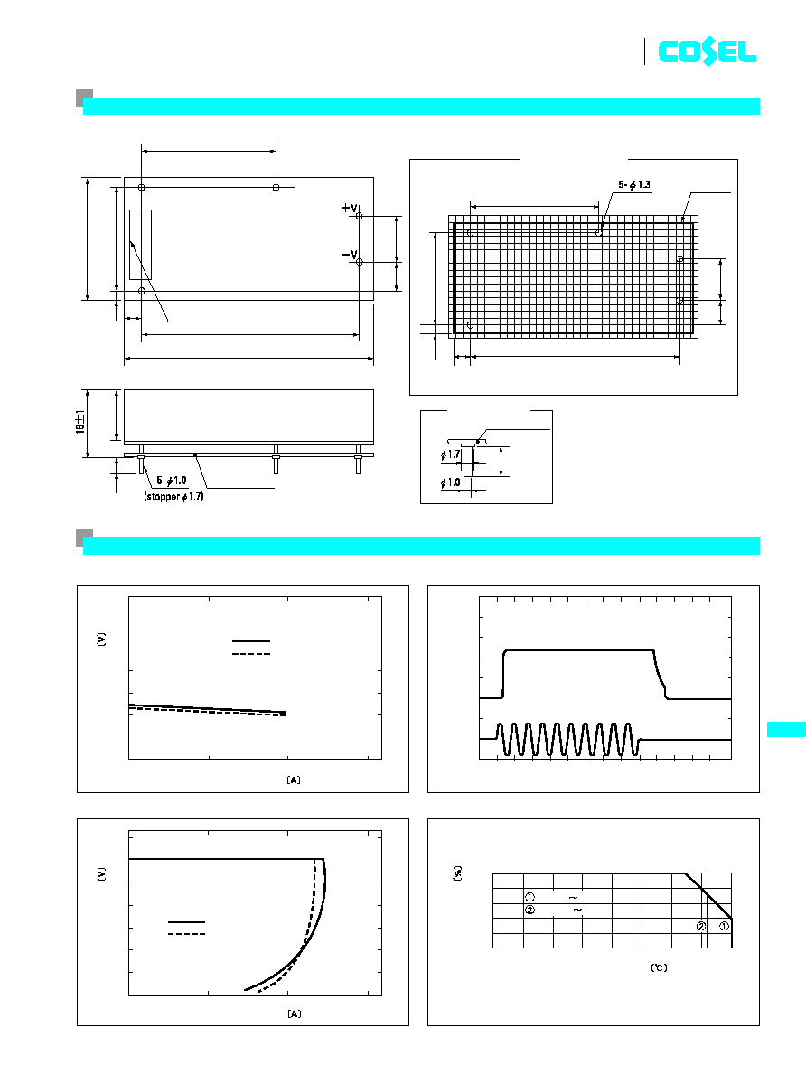
VAA5
External view
∂
Dimension: mm
∂
Unit: 2mm
∂
Weight: 30g or Less
∂
Tolerance:
±
0.5
∂
PCB material: CEM-3
∂
PCB thickness: t=1.0
∂
Pin material: CPW with solder plated
∂
Bottom cover material: Bake PL 1256 (Black)
∂
Recommended hole dia. to PCB:
∫
1.3
Recommended size for
processing PCB
(TOP VIEW)
35
57
4.5
65
32
12
7.5
27
(TOP VIEW)
FG
AC
AC
35
Outline
57
4.5
12
7.5
27
2.5
2.5
(13.5)
4
bottom cover
bottom cover
4
Input/Output Pin
Name Plate
Performance data

MODEL
VAA1005
VAA1012
MAX OUTPUT WATTAGE[W]
10.0
10.8
DC OUTPUT
VOLTAGE[V] 5
12
CURRENT[A] 2.0
0.9
SPECIFICATIONS
MODEL
VAA1005
VAA1012
INPUT
VOLTAGE[V]
AC85 - 132 1
f
or DC110 - 170
CURRENT[A]
*
1
0.3typ (ACIN 100V, Io=100%)
EFFICIENCY[%]
*
1
76typ
77typ
FREQUENCY[Hz]
47 - 440 or DC
INRUSH CURRENT[A]
*
1
15typ (ACIN 100V, Io=100%)
LEAKAGE CURRENT[mA] 0.5max (60Hz According to UL and DEN-AN)
OUTPUT
VOLTAGE[V]
5
12
CURRENT[A]
2.0
0.9
LINE REGULATION[mV]
20max
48max
LOAD REGULATION[mV] 40max
100max
RIPPLE[mVp-p]
0 to +55
C
*
2
80max
120max
-10 - 0
C
*
2
140max
160max
RIPPLE NOISE[mVp-p]
0 to +55
C
*
2
120max
150max
-10 - 0
C
*
2
160max
180max
TEMPERATURE COEFFICIENT[mV] -10 to +55
C
50max
120max
DRIFT[mV]
*
3
20max
48max
OUTPUT VOLTAGE ADJUSTMENT RANGE Fixed
START-UP TIME[ms]
200max (ACIN 85V, Io=100%)
HOLD-UP TIME[ms]
10typ (ACIN 85V, Io=100%), 20typ (ACIN 100V, Io=100%)
OUTPUT VOLTAGE SETTING[V]
*
1
4.90 - 5.30
11.40 - 12.60
PROTECTION
CIRCUIT
OVERCURRENT PROTECTION Works over 105% of rating and recovers automatically
OVERVOLTAGE PROTECTION
Works over 115% of rating (by zener diode clamping)
ISOLATION
INPUT-OUTPUT
AC2,000V 1minute, Cutoff current = 10mA, DC500V 50M
W
min (At Room Temperature)
INPUT-FG
AC2,000V 1minute, Cutoff current = 10mA, DC500V 50M
W
min (At Room Temperature)
OUTPUT-FG
AC500V 1minute, Cutoff current = 100mA, DC500V 50M
W
min (At Room Temperature)
ENVIRONMENT
OPERATING TEMP.,HUMID.AND ALTITUDE -10 to +70
C
, 20 - 90%RH (Non condensing) (Refer to DERATING CURVE), 3,000m (10,000feet) max
STORAGE TEMP.,HUMID.AND ALTITUDE -20 to +75
C
, 20 - 90%RH (Non condensing), 9,000m (30,000feet) max
VIBRATION
19.6m/s
2
10 - 55Hz, 3minutes period, 60minutes each along X, Y and Z axis (Non operating)
IMPACT
196.1m/s
2
11ms, once each X, Y and Z axis (Non operating)
SAFETY AND
NOISE
REGULATIONS
AGENCY APPROVALS
UL60950-1, C-UL Complies with DEN-AN (External Fuse is required)
CONDUCTED NOISE
Complies with FCC-B, additional capacitors required for meeting VCCI class B
OTHERS
CASE SIZE/WEIGHT
32
X
18
X
72.5mm (W
X
H
X
D) / 35g max
COOLING METHOD
Convection
*
1
Rated input/output Ta=25
C
*
2
This is the value that measured on measuring board with capacitor of 22
m
F. Measured by 20MHz oscilloscope or Ripple-Noise meter (Equivalent to KEISOKU-GIKEN: RM101).
*
3
Drift is the charge in DC output for an eight hour period after a half-hour warm-up at 25
C
, with the input voltage held constant at the rated input/output.
VAA10
On-board type
VAA
10
05
Ordering information
1
Series name
2
Output wattage
3
Output voltage
R
1
2
3
VAA
G-158

°
DERATING CURVE
°
RISE TIME & FALL TIME (VAA1012)
°
OVERCURRENT CHARACTERISTICS (VAA1012)
°
STATIC CHARACTERISTICS (VAA1012)
Input Voltage AC 85V
0.5
0
12.03
12.05
12.07
1.0
1.5
Input Voltage AC132V
OUTPUT V
O
L
T
A
G
E
OUTPUT CURRENT
DC Output
AC Input
ACIN 85V Io=100%
20ms/DIV
5V/DIV
0.5
0
2
4
6
8
10
12
14
1.0
1.5
Input Voltage AC 85V
Input Voltage AC132V
ACIN85 115V
ACIN116 132V
OUTPUT V
O
L
T
A
G
E
OUTPUT CURRENT
-10
0
10
20
30
40
50
60
70
0
20
40
60
80
100
LO
AD FA
CT
OR
AMBIENT TEMPERATURE
VAA
G-159
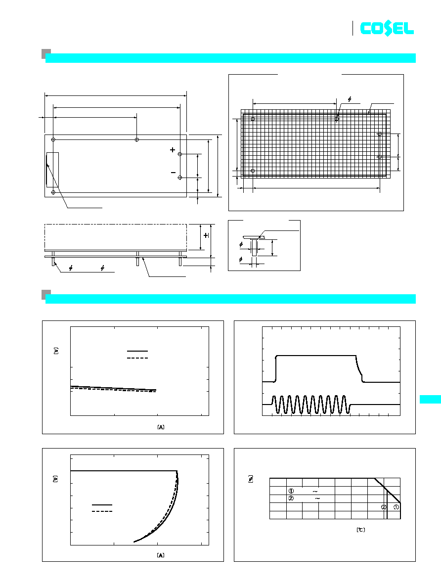
VAA10
External view
∂
Dimension: mm
∂
Unit: 2mm
∂
Weight: 35g or Less
∂
Tolerance:
±
0.5
∂
PCB material: CEM-3
∂
PCB thickness: t=1.0
∂
Pin material: CPW with solder plated
∂
Bottom cover material: Bake PL 1256 (Black)
∂
Recommended hole dia. to PCB:
∫
1.3
Recommended size for
processing PCB
(TOP VIEW)
72.5
64.5
42.5
4.5
32
27
AC
AC
42.5
5- 1.3
Outline
64.5
4.5
12
7.5
27
2.5
2.5
(13.5)
18 1
4
5- 1.0
bottom cover
bottom cover
(stopper 1.7)
12
7.5
(TOP VIEW)
FG
1.7
1.0
4
Input/Output Pin
V
V
Name Plate
Performance data

