c
2004
cosmo
ELECTRONICS CORPORATION
http://www.cosmo-ic.com
28
Absolute Maximum Ratings
Electrical Characteristics
Parameter
Symbol
Conditions
MIN
TYP MAX
Unit
Input
Pick-up Voltage
Vpu
It=1Arms
4
VDC
Input current
Iin
Vin=5-12V
5
25
mA
On-state Voltage
V
T
I
T
=1Arms
1.5
Vrms
Operating Current
Iop
Vout=240Vrms
50
Leakage Current
I leak
Vout=240Vrms
7
Critical rate of rise of off-state Voltage
dv/dt
See Note 1
50
200
Zero-cross Voltage
Yes
Load Voltage Rating
Vout
I
T
=50mArms MIN
50
280
VAC
Minimum trigger current
I
FT
V
DRM
=600V
10
mA
Isolation resistance input to output
R
ISO
DC500V
10
10
Turn-on time
Ton
60Hz AC
8.3
mS
Turn-off time
Toff
60Hz AC
8.3
mS
Thermal resistance (between junction and case)
Rth (j-C) I
1.3
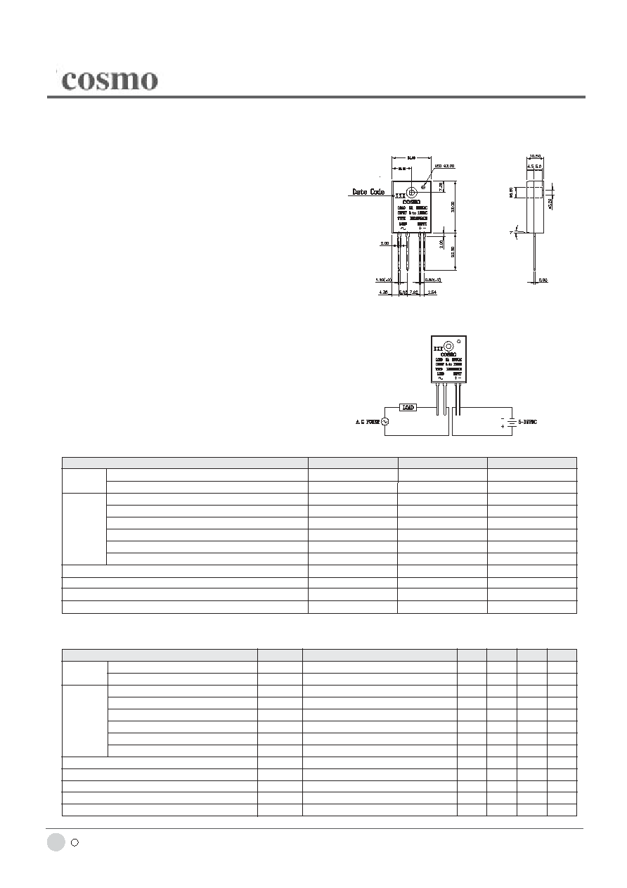
KSD205AC3
Solid State Relay
Outside Dimension : Unit
(mm)
Schematic : Top View
Features
1. Molded epoxy body.
2. Zero crossing circuit.
3. High input/output insulation.
4. Small size and light weight.
5. Can be installed directly on the PC board.
6. Fast reactive speed.
7. Normally open.
Applications
1. Household Appliances.
2. Temperature Control System.
3. Industrial Automatic Control.
4. Lighting System.
5. Office Appliances.
6. Factory Appliances.
Parameter
Symbol
Rating Unit
Input
Input Signal Voltage
V
IN
5~12
VDC
Drop-out Voltage
Vdo
1
VDC
RMS on-state current
I
T
5
Arms
Peak one cycle surge current (8.3 ms)
Isurge
50
A
Repetitive peak-off state Voltage
V
DRM
600
V
Operating frequency
f
47~70
Hz
Critical rate of rise of on-state current
di/dt
50
Load supply voltage
Vout
250
Vrms AC
Isolation Voltage input to output
Viso
4000
Vrms
Operating Temperature
Topr
-30~100
Storage Temperature
Tstg
-30~125
Soldering Temperature 10 Sec
Tsol
260
Output
(Ta=25
∞
C)
(Ta=25
∞
C)
A/
S
V/
S
Output
mArms
mArms
Note1
Output (dv/dt) protection is provided in all models, and they are designed to switch resistive or inductive loads to 0.2 power factor. The dv/dt rating is based on source impedance of 50 ohms.
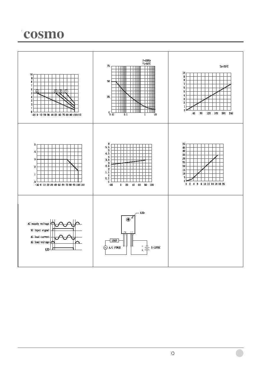
Fig.8 WIRING DIAGRAM
Ambient Temperature Ta (
∞
C)
Input V
o
ltage (V)
Fig.5 Input Voltage vs. Ambient Temperature
Input Voltage (VDC)
Input Current (mA)
Fig.6 Input Current vs. Input voltage
Time (SEC)
Surge Current (A)
Fig.2 Surge Current vs. Time
Supply Voltage (Vrms)
Open Circuit Leak Current ILeak (mArms)
Fig.3 Open Circuit Leak Current vs.
Supply Voltage
Case Temperature Tc (
∞
C)
RMS On-state Current (A)
Fig.4 RMS On-state Current vs.
CaseTemperature
Fig.7 Action waveform
KSD205AC3
c
2004
cosmo
ELECTRONICS CORPORATION
http://www.cosmo-ic.com
29
Data Curve
Ambient Temperature Ta (
∞
C)
RMS On-state Current (A)
Fig.1 RMS On-state Current vs. Ambient
Temperature
(1) With infinite heat sink
(2) With heat sink (70x70x2mm AI plate)
(3) With heat sink (50x50x2mm AI plate)
(4) Without heat sink