G
∑
SiC
Æ
Technology
XThinTM LEDs
CxxxXT290-S0100-A
Features Applications
∑ XThin
TM
Performance
≠ 12.0 mW min.
∑ Thin 115µm Chip
∑ Low Forward Voltage
≠ 3.2 Typical at 20mA
∑ Single Wire Bond Structure
∑ Class II ESD Rating
∑ Cellular Phone LCD Backlighting
∑ Digital Camera Flash For Mobile Appliance
∑ Mobile Phone Key Pads
White LEDs
Blue LEDs
∑ Automotive Dashboard Lighting
∑ LED Video Displays
∑ Audio Product Display Lighting
Description
Cree's XThinTM LEDs are the next generation of solid state LED emitters that combine highly efficient
InGaN materials with Cree's proprietary G∑SiCÆ substrate to deliver superior price performance for
high intensity LEDs. These LED chips have a geometrically enhanced Epi-down design to maximize
light extraction efficiency, and require only a single wire bond connection. These vertically structured
LED chips are approximately 115 microns in height and require a low forward voltage. Cree's XT chips
are tested for conformity to optical and electrical specifications and the ability to withstand 1000V ESD.
Applications for XThin include next generation mobile appliances for use in their LCD backlights and
digital camera flash where brightness, sub-miniaturization, and low power consumption are required.
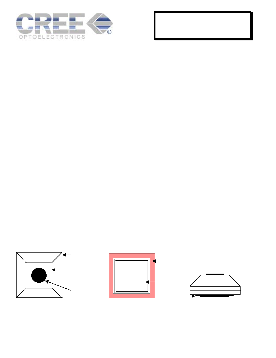
CxxxXT290-S0100-A Chip Diagram
G
300 x 300 µm
∑
SiCÆ LED Chip
Top Area
200 x 200 µm
Cathode (-)
h = 115 µm
Backside
Metallization
210 x 210 µm
Anode (+)
InGaN
SiC Substrate
Bottom View
Die Cross Section
Junction Area
248 x 248 µm
Bond Pad
105µm Dia.
Top View
CPR3BV Rev.-
© Cree, Inc. 2003 All Rights Reserved

G
∑
SiC
Æ
Technology
XThinTM LEDs
CxxxXT290-S0100-A
Maximum Ratings at T
A
= 25∞C
Notes 1&3
CxxxXT290-S0100-A
DC Forward Current
30mA
Peak Forward Current (1/10 duty cycle @ 1kHz)
100mA
LED Junction Temperature
125∞C
Reverse Voltage
5 V
Operating Temperature Range
-40∞C to +100∞C
Storage Temperature Range
-40∞C to +100∞C
Electrostatic Discharge Threshold (HBM)
Note 2
1000V
Electrostatic Discharge Classification (MIL-STD-883E)
Note 2
Class
2
Typical Electrical/Optical Characteristics at T
A
= 25∞C, If = 20mA
Note 3
Part number
Forward Voltage (V
f,
V)
Reverse Current
[I(Vr=5V), µA]
Min Typ Max
Max
C460XT290-S0100-A
2.7
3.2 3.7
10
C470XT290-S0100-A
2.7 3.2 3.7
10
Mechanical Specifications
CxxxXT290-S0100-A
Description Dimension
Tolerance
P-N Junction Area (µm)
248 x 248
± 25
Top Area (µm)
200 x 200
± 25
Bottom Area (Substrate) (µm)
300 x 300
± 25
Chip Thickness (µm)
115
± 15
Au Bond Pad Diameter (µm)
105
-5, +15
Au Bond Pad Thickness (µm)
1.2
± 0.5
Back Contact Metal Area (µm)
210 x 210
± 25
Back Contact Metal Thickness (µm) (Au/Sn)
Note 4
1.7 ±
0.3
Notes:
1) Maximum ratings are package dependent. The above ratings were determined using a T-1 3/4 package (with Hysol
OS4000 epoxy) for characterization. Seller makes no representations regarding ratings for packages other than the T-1
3/4 package used by Seller. The forward currents (DC and Peak) are not limited by the G ∑SiC die but by the effect of
the LED junction temperature on the package. The junction temperature limit of 125∞C is a limit of the T-1 3/4 package;
junction temperature should be characterized in a specific package to determine limitations. Assembly processing
temperature must not exceed 325∞C (< 5 seconds). See Cree XBright Applications Note for more assembly process
information.
2) Product resistance to electrostatic discharge (ESD) is measured by simulating ESD using a rapid avalanche energy test
(RAET). The RAET procedures are designed to approximate the maximum ESD ratings shown. Seller gives no other
assurances regarding the ability of Products to withstand ESD.
3) All Products conform to the listed minimum and maximum specifications for electrical and optical characteristics, when
assembled and operated at 20 mA within the maximum ratings shown above. Efficiency decreases at higher currents.
Typical values given are the average values expected by Seller in large quantities and are provided for information only.
Seller gives no assurances Products shipped will exhibit such typical ratings. All measurements were made using lamps
in T-1 3/4 packages (with Hysol OS4000 epoxy). Dominant wavelength measurements taken using Illuminance E.
4) Back contact metal is 80%/20% Au/Sn by weight, with target eutectic melting temperature of approximately 282∞C. See
XBright Applications Note for detailed packaging recommendations.
5) Caution: To avoid leakage currents and achieve maximum output efficiency, die attach material must not contact the
side of the chip. See Cree XBright Applications Note for more information.
CPR3BV Rev.-
© Cree, Inc. 2003 All Rights Reserved

G
∑
SiC
Æ
Technology
XThinTM LEDs
CxxxXT290-S0100-A
Standard Bins for XT290:
All LED chips are sorted onto die sheets according to the bins shown below. All radiant flux and all
dominant wavelength values shown and specified are at If = 20mA.
C460XT290-S0100-A
C470XT290-S0100-A
C460XT290-0108-A
C470XT290-0108-A
C460XT290-0103-A
C460XT290-0105-A
C460XT290-0106-A
C460XT290-0107-A
C470XT290-0106-A
C470XT290-0107-A
C460XT290-0101-A
Sorted Die Kits may contain any or all
bins shown to the left.
C460XT290-0104-A
470nm
472.5nm
Dominant Wavelength
462.5nm
C470XT290-0102-A
C470XT290-0103-A
C470XT290-0104-A
457.5nm
C460XT290-0102-A
460nm
15.0mW
12.0mW
455nm
Radiant Flux
Radiant Flux
15.0mW
12.0mW
465nm
C470XT290-0101-A
C470XT290-0105-A
467.5nm
465nm
Sorted Die Kits may contain any or all
bins shown to the left.
Dominant Wavelength
475nm
CPR3BV Rev.-
© Cree, Inc. 2003 All Rights Reserved

CPR3BV Rev.-
© Cree, Inc. 2003 All Rights Reserved
G
∑
SiC
Æ
Technology
XThinTM LEDs
CxxxXT290-S0100-A
Characteristic Curves:
These are representative measurements for the XThin product. Actual curves will vary slightly for the
various radiant flux and dominant wavelength bins.
Forward Current vs. Forward Voltage
0
5
10
15
20
25
30
0.0
0.5
1.0
1.5
2.0
2.5
3.0
3.5
4.0
4.5
5.0
Vf (V)
If
(
m
A
)
Wavelength Shift vs Forward Current
-2.0
0.0
2.0
4.0
6.0
8.0
10.0
0
5
10
15
20
25
30
If(mA)
S
h
i
ft (nm
)
Relative Intensity vs Forward Current
0
20
40
60
80
100
120
140
0
5
10
15
20
25
30
If(mA)
% Int
e
nsit
y
Relative Intensity vs Peak Wavelength
Relat
i
ve Int
e
nsit
y (
%
)
Wavelength (nm)
400
500
600
20
40
60
80
100