 | –≠–ª–µ–∫—Ç—Ä–æ–Ω–Ω—ã–π –∫–æ–º–ø–æ–Ω–µ–Ω—Ç: UGF18060 | –°–∫–∞—á–∞—Ç—å:  PDF PDF  ZIP ZIP |
Rev 2.
UGF18060
UGF18060
60W, 1.8 GHz, 26V Broadband RF Power N-Channel
Enhancement-Mode Lateral MOSFET
Designed for DCS base station applications in the frequency band 1.805 to 1.88 GHz. Rated with
a minimum output power of 60W. It is ideal for CDMA, TDMA, WCDMA, GSM, and Multi-Carrier
Power Amplifiers in Class AB operation.
∑
∑
∑
∑
∑
∑
ALL GOLD metal system for highest reliability
Industry standard package
Suggested alternative to the MRF18060
Internally matched for repeatable manufacturing
High gain, high efficiency and high linearity
Application Specific Performance, 1.88 GHz
GSM:
60 Watts
12.5 dB
EDGE:
25 Watts
12.5 dB
IS95 CDMA:
7.5 Watts
12.5 dB
CDMA2000:
TBD Watts
12.5 dB
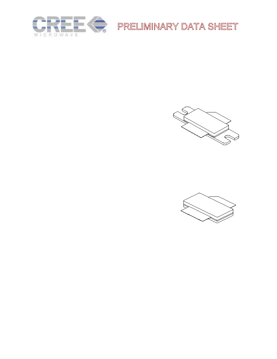
Package Type 440172
PN: UGF18060P
Package Type 440171
PN: UGF18060F
Rev 2.
UGF18060
UGF18060
Maximum Ratings
Rating Symbol
Value
Unit
Drain to Source Voltage, Gate connected to Source
V
DSS
65
Volts
Gate to Source Voltage
V
GSS
+15 to ≠0.5
Volts
Total Device Dissipation @ Tcase = 60
o
C
Derate above 60
o
C
P
D
65
0.83
Watts
W/
o
C
Storage Temperature Range
T
stg
-65 to +150
o
C
Operating Junction Temperature
T
J
200
o
C
Thermal Characteristics
Characteristic Symbol
Typical
Unit
Thermal Resistance, Junction to Case
JC
-
o
C/W
Electrical DC Characteristics
(T
C
=25
∞
C unless otherwise specified)
Rating Symbol
Min
Typ
Max
Unit
Drain to Source Breakdown Voltage
(V
GS
=0, I
D
=1mA)
BV
DSS
65 - -
Volts
Drain to Source Leakage current
(V
DS
=26V, V
GS
=0)
I
DSS
- -
1.0
mA
Gate to Source Leakage current
(V
GS
=15V, V
DS
=0)
I
GSS
- -
1.0
µ
A
Threshold Voltage
(V
DS
=10V, I
D
=1mA)
V
GS(th)
- 3.5
-
Volts
Gate Quiescent Voltage
(V
DS
=26 V, I
D
=900mA)
V
GS(Q)
3.0 4.0
6.0
Volts
Drain to Source On Voltage
(V
GS
=10V, I
D
=2A)
V
DS(on)
- 0.15
-
Volts
Forward Transconductance
(V
DS
=10V, I
D
=5A)
Gm - -
-
S
AC Characteristics
(T
C
=25
∞
C unless otherwise specified)
Rating Symbol
Min
Typ
Max
Unit
Input Capacitance *
(V
DS
=26V, V
GS
=0V, f = 1MHz)
C
ISS
- -
-
pF
Output capacitance *
(V
DS
= 26V, V
GS
=0V, f = 1MHz)
C
OSS
- 350
-
pF
Feedback capacitance *
(V
DS
=26V, V
GS
=0V, f = 1MHz)
C
RSS
- -
-
pF
* Part is internally matched on input and output.

Rev 2.
UGF18060
UGF18060
RF and Functional Tests
(Tc=25
∞
C unless otherwise specified, Cree Microwave Broadband Fixture)
Rating Symbol
Min
Typ
Max
Unit
CW Small Signal Gain, Pout=10W
V
DD
=26V, I
DQ
=500mA
G
L
-
12.5
-
dB
CW Power Gain, P
out
= 60 W
V
DD
=26V, I
DQ
=500mA
G
P
-
11.5
-
dB
CW Drain Efficiency, P
out
= 60 W,
f=1880 MHz, V
DD
=26V, I
DQ
=500mA,
D
- 36
-
%
Two-Tone Common-Source Amplifier Power Gain
V
DD
=26V, I
DQ
=500mA, P
out
= 60 W PEP
f
1
=1880 MHz and f
2
=1880.1 MHz
G
TT
- 12
-
dB
Two-Tone Intermodulation Distortion
V
DD
=26V, I
DQ
=500mA, P
out
= 60 W PEP
f
1
=1880 MHz and f
2
=1880.1 MHz
I
MD
-
-28
-
dBc
Two-Tone Drain Efficiency
V
DD
=26V, I
DQ
=500mA, P
out
= 60 W PEP
f
1
=1880 MHz and f
2
=1880.1 MHz
D2
- 38
-
%
Input Return Loss
V
DD
=26V, P
out
= 60 W PEP, I
DQ
=500mA
f
1
=1805 MHz and 1880 MHz, Tone Spacing =
100kHz
IRL -
-10
-
dB
Load Mismatch Tolerance
V
DS
=26V, I
DQ
= 500 mA, Pout=60W, f=1880 MHz
VSWR* 10:1 - -
Note (unless otherwise specified):
1. Source and load impedance shall be 50 ohms.
*No degradation in device performance after test.
CAUTION - MOS Devices are susceptible to damage from Electrostatic Discharge (ESD). Appropriate
precautions in handling, packaging and testing MOS devices must be observed.
Rev 2.
UGF18060
UGF18060
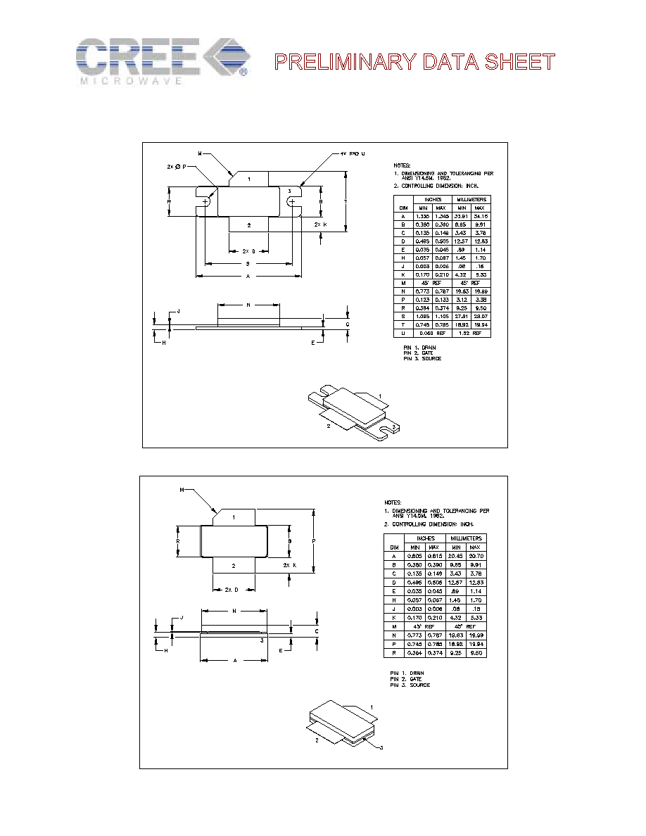
Product Dimensions
Package Number 440171
Package Number 440172