 | –≠–ª–µ–∫—Ç—Ä–æ–Ω–Ω—ã–π –∫–æ–º–ø–æ–Ω–µ–Ω—Ç: UGF19125 | –°–∫–∞—á–∞—Ç—å:  PDF PDF  ZIP ZIP |

UGF19125
∑
∑
∑
∑
Designed for W-CDMA base station applications at frequency bands from 1.9 to 2.0 GHz.
Suitable for TDMA, N-CDMA, W-CDMA, GSM and Multi-Carrier power amplifiers in class AB
operation for PCN and PCS /Cellular radio applications.
∑
∑
∑
∑
∑
Internally matched for repeatable manufacturing.
ALL GOLD metal system for highest reliability.
Suggested alternative to the MRF19125/MRF19125S.
Integrated ESD protection.
High gain, high efficiency and high linearity.
Industry standard package.
Maximum gain and insertion phase flatness.
Capable of handling 10:1 VSWR, @ 28 Vdc, 1930 MHz,
125W (CW) Output Power.
Excellent thermal stability.
Package Type 440174
PN: UGF19125F
Package Type 440175
PN: UGF19125P
∑
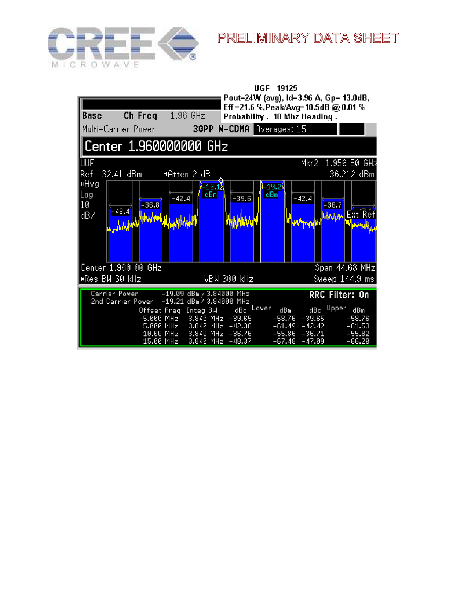
Typical 2-Carrier W-CDMA Performance
f1 = 1955MHz, f2 = 1965MHz
Average Output Power = 24 W
Efficiency = 22%
Power Gain = 13.0 dB
IM3 = -36.7 dBc (3.84 MHz BW @ f1-10MHz and f2+10MHz)
ACPR = -43dBc (3.84 MHz BW @ f1-5MHz and f2+5MHz)
V
DD
= 28V
I
DQ
= 1300mA
Peak/Avg. = 10.5dB @ 0.01% Probability on CCDF
125W, 2.0 GHz, 26V, Broadband RF Power N-Channel
Enhancement-Mode Lateral MOSFET
UGF19125 Rev. 1

Maximum Ratings
Rating Symbol
Value
Unit
Drain to Source Voltage
V
DSS
65 Volts
Gate to Source Voltage
V
GSS
+15
/-0.5 Volts
Total Device Dissipation @ Tcase = 25
o
C
Derate above 25
o
C
P
D
219
1.25
Watts
W/
o
C
Storage Temperature Range
T
STG
-60 to +150
o
C
Maximum JunctionTemperature
T
J
200
o
C
Thermal Characteristics
Characteristics Symbol
Max
Unit
Thermal Resistance, Junction to Case, is a maximum of
jc
0.80
o
C/W
Electrical DC Characteristics
(Tc=25
∞C unless otherwise specified)
Rating Symbol
Min
Typ
Max
Unit
Drain to Source Breakdown Voltage
(V
GS
=0, I
D
=1mA)
BV
DSS
65 73
-
Volts
Drain to Source Leakage Current
(V
GS
=28 V
DC
, V
GS
=0 V
DC
)
I
DSS
- -
10
mA
Drain to Source Leakage Current
(V
DS
=65V
DC
, V
GS
=0 V
DC
)
I
DSS
- -
180
µA
Gate to Source Leakage Current, Forward
(V
GS
=15V
DC
, V
DS
=0 V
DC
)
I
GSSF
- -
1.0
µA
Threshold Voltage
(V
DS
= V
GS
, I
D
=20mA)
V
GS(th)
2.7 -
5.0
Volts
Threshold Voltage
(V
DS
= V
GS
, I
D
=1mA)
V
GS(th)
2.4 -
5.0
Volts
Gate Quiescent Voltage
(V
DS
=28 V
DC
, I
D
=1300mA)
V
GS(Q)
3 3.7
4.5
Volts
Drain to Source On Voltage
(V
GS
=10 V
DC
, I
D
=1A
V
DS(on)
-
0.075
0.12
Volts
Forward Transconductance
(V
DS
=10 V
DC
, I
D
=1.0A)
Gm 1.0 -
-
S
Notes (unless otherwise specified):
1. All tests are at 25
∞C.
AC Characteristics
(Tc=25
∞C unless otherwise specified)
Rating Symbol
Min
Typ
Max
Unit
Input capacitance *
(V
DS
=28V, V
GS
=0V, f = 1MHz)
C
ISS
- 360 -
pF
Output capacitance
(V
DS
=28V, V
GS
=0V, f = 1MHz)
C
OSS
- TBD -
pF
Feedback capacitance *
(V
DS
=28V, V
GS
=0V, f = 1MHz)
C
RSS
-
3.8
- pF
* Part is internally matched.
UGF19125 Rev. 1

RF and Functional Tests
(Tc=25
∞C unless otherwise specified, Cree Microwave Broadband Fixture)
Rating Symbol
Min
Typ
Max
Unit
Power Gain, P
OUT
=125W, CW 51dBm
V
DD
=28V, I
DQ
=1.3A
f= 1930-1990 MHz
G
P
10 -
15
dB
Power Gain, P
OUT
=31.5W, CW 45dBm
V
DD
=28V, I
DQ
=1.3A
f= 1930-1990 MHz
G
L
11
-
15
dB
Drain Current, P
OUT
=125W, CW 51dBm
V
DD
=28V, I
DQ
=1.3A
f= 1930-1990 MHz
I
D
-
-
12
A
Two-Tone Drain Efficiency
V
DD
= 28 V, I
DQ
= 1.3 A, P
OUT
= 125W PEP
f =1930 - 1990 MHz, Tone Spacing =100kHz
D
- 35.0
30
%
Two-Tone Common-Source Amplifier Power Gain
V
DD
= 28V, I
DQ
= 1.3A, P
OUT
= 125W PEP
f
1
=1990MHz and f
2
= 1990.1 MHz
G
TT
11 - -
dB
Two-Tone Third Order Intermodulation Distortion
V
DD
= 28V, I
DQ
= 1.3A, P
OUT
= 125W PEP
f
1
= 1990 MHz and f
2
= 1990.1 MHz.
IMD3
-
- -28
dBc
Two-Tone Drain Efficiency
V
DD
= 28 V, I
DQ
= 1.3 A, P
OUT
= 125W PEP
f
1
=1990 MHz and f
2
=1990.1 MHz
D2
- 35.5
30
%
Two Tone Drain Current, P
OUT
= 51 dBm
125W PEP, f
1
=1990 MHz and f
2
=1990.1 MHz
I
MD3
- -
7.3
A
Input Return Loss
V
DD
= 28 V, I
DQ
= 1.3 A, P
OUT
= 125W PEP
f = 1990MHz, Tone Spacing =100kHz
IRL 7.5 - -
dB
Load Mismatch Tolerance*
V
DD
= 28V, I
DQ
= 1.3 A, P
OUT
=125W, f=1930MHz
VSWR 10:1 - -
Note (unless otherwise specified):
1. Source and load impedance shall be 50 ohms.
*No degradation in device performance after test.
CAUTION - MOS Devices are susceptible to damage from Electrostatic Discharge (ESD). Appropriate
precautions in handling, packaging and testing MOS devices must be observed.
UGF19125 Rev. 1
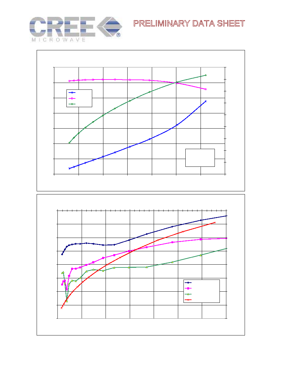
Power Gain, Efficiency vs Output Power
0
2
4
6
8
10
12
14
0
20
40
60
80
100
120
140
Output Power (Watts) CW Avg.
Pin (Watts), GP Power Gain (dB)
0
5
10
15
20
25
30
35
40
45
Drain Efficiency (%)
PIn(w)
Gp(dB)
EFF(%)
V
DD
= 28V
DC
I
DQ
= 1300mA
Freq = 1960MHz
Intermodulation Distortion Products, Drain Efficiency vs Output Power
-100
-90
-80
-70
-60
-50
-40
-30
-20
0
20
40
60
80
100
120
140
Pout, Output Power (Watts) PEP
IMD, Intermodulation Distortion (dBc)
0
5
10
15
20
25
30
35
40
Drain Efficiency (%)
3rd Order IMD
5th Order IMD
7th Order IMD
EFF(%, Avg)
UGF19125 Rev. 1
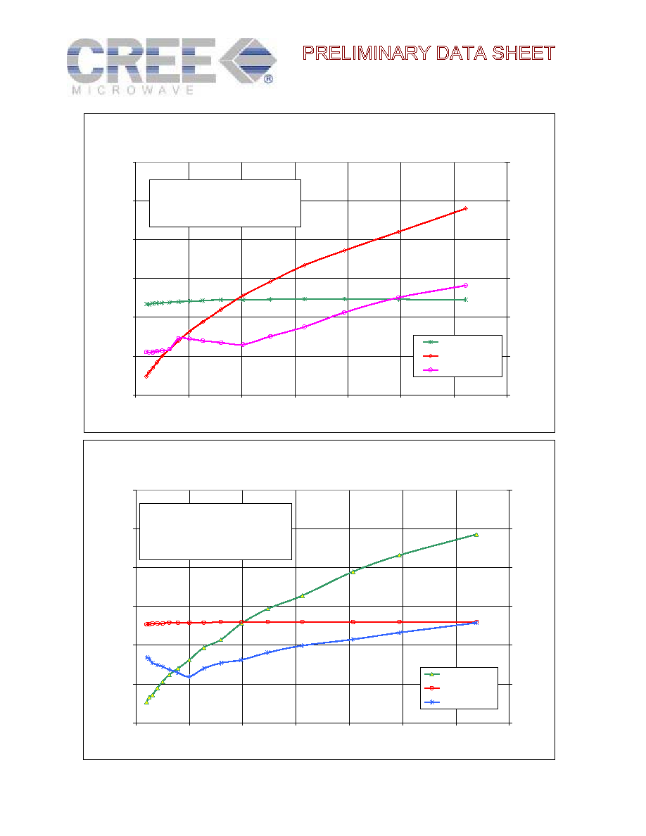
Two Carriers N-CDMA
IM3, Power Gain, Drain Efficiency vs Output Power
0
5
10
15
20
25
30
0
5
10
15
20
25
30
35
Pout, Output Power (Watts) N-CDMA
Drain Efficiency (%),
Gps, Power Gain (dB)
-60
-50
-40
-30
-20
-10
0
IM3 (dBc)
Gp(dB)
EFF(%, Avg)
IM3
V
DD
= 28V
DC
, I
DQ
= 1300mA
Freq = 1960MHz
1.23MHz Channel Bandwidth
Peak/Avg. = 10.5dB @ 0.01% Probability
Two Carriers W-CDMA
IM3, Power Gain and Drain Efficiency vs Output Power
0
5
10
15
20
25
30
0
5
10
15
20
25
30
35
Pout, Output Power (Watts Avg) WCDMA
Dr
ain Ef
f
i
ciency (
%
)
,
Gps, Power Gain (dB)
-60
-50
-40
-30
-20
-10
0
IM3 (dBc)
EFF(%, Avg)
Gp(dB)
IM3
V
DD
= 28V
DC
, I
DQ
= 1300mA
Freq = 1960MHz
3.84MHz Channel Bandwidth
Peak/Avg. = 10.5dB @ 0.01% Probability
10MHz Spacing
UGF19125 Rev. 1
UGF19125 Rev. 1