
© 2006 CTS Corporation. All rights reserved. Information subject to change.
CTS Electronic Components
Page 1
April 06
www.ctscorp.com
LDS & LVPECL FPGA Terminator
Style C
Style I
R1
R1
R1
R1
A
C
D
E
B
F
G
H
1
R1
R1
R1
R1
2
3
4
R1
R1
R1
R1
R1
R1
R1
R1
R1
R1
R1
R1
A
C
D
E
B
F
G
H
1
R1
R1
R1
R1
2
3
4
R1
R1
R1
R1
R1
R1
R1
R1
R1
R1
R1
R1
A
C
D
E
B
F
G
H
1
R1
R1
R1
R1
2
3
4
R1
R1
R1
R1
R1
R1
R1
R1
R1
R1
R1
R1
A
C
D
E
B
F
G
H
1
R1
R1
R1
R1
2
3
4
R1
R1
R1
R1
R1
R1
R1
R1
R2
R2
R2
R2
R2
R2
R2
R2
R1
R1
R1
R1
J
L
M
N
K
P
R
T
R1
R1
R1
R1
R1
R1
R1
R1
R1
R1
R1
R1
R2
R2
R2
R2
R2
R2
R2
R2
Electrical Specifications
Tx Termination
Rx Termination
R1
R1
R1
R2
Z = 50 ohms
Tx
Rx
Typical Application
Features
∑
Designed for termination of Xilinx
Æ
and Altera
Æ
FPGAs.
∑
8 or 16 differential channels of termination provided in a single
integrated package
∑
Excellent high frequency performance
∑
High density ceramic BGA package
∑
RoHS Compliant Designs Available
∑
Compatible with both lead and lead-free manufacturing
processes
Ordering Information
1.27mm Pitch
Standard Part
No.
1.00mm Pitch
Standard Part
No.
Style R1
R2
Array
Size
1.27mm Pitch
RoHS Part No.
1.00mm Pitch
RoHS Part No.
RT1710B6
RT1710B7
C
100
-
4 x 8
RT2710B6
RT2710B7
-
RT1720B7
I
187
100
4 x 16
-
RT2720B7
RT1721B6
RT1721B7
I
187
100
4 x 8
RT2721B6
RT2721B7
-
RT1722B7
I
140
165
4 x 16
-
RT2722B7
RT1723B6
RT1723B7
I
140
165
4 x 8
RT2723B6
RT2723B7
-
RT1724B7
I
140
135
4 x 16
-
RT2724B7
RT1725B6
RT1725B7
I
140
135
4 x 8
RT2725B6
RT2725B7
Description
These LVPECL and LVDS termination networks are designed for high
performance termination of differential Input/Output signals on some of
the most popular Field Programmable Gate Arrays (FPGAs).
Both input (RX) and output (TX) termination is provided.
LVDS & LVPECL FPGA Terminator
Technical
Data Sheet
RoHS Compliant Parts Available
Resistor Tolerance:
±
1.0%
TCR
±
200ppm/
∞
C
Operating Temperature Range
-55
∞
C to +125
∞
C
Maximum Resistor Power:
0.068 Watts at 70
∞
C
Maximum Package Power:
1.0 Watts at 70
∞
C
Process Requirements:
Maximum Re-flow Temperature
Per IPC/JEDEC J-STD-020C
Packaging Information
Suffix
TR7
TR13
Tape Width
24 mm
24mm
Carrier Pitch
8 mm
8 mm
Reel Diameter
7 inch
13 inch
Parts/Reel
1,000 4,000
Part Number Coding
7 inch reel, Add TR7 to part
number, example RT2400B6TR7
13 inch reel, Add TR13 to part
number, example RT2400B6TR13
(Bulk packaging is not available)
Direction of Feed
© 2006 CTS Corporation. All rights reserved. Information subject to change.
CTS Electronic Components
Page 2
April 06
www.ctscorp.com
LDS & LVPECL FPGA Terminator
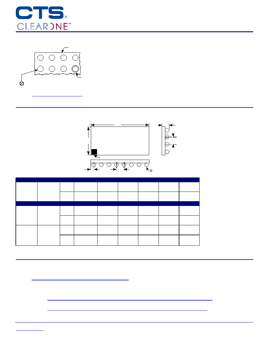
Recommended Land Pattern
1.00mm Pitch (B7) = 0.51mm/.020 inch (minimum)
Outline of Substrate
PCB Pad Diameter
For .006" Thick Solder Paste Stencil, Aperture Opening Should
be Equal to the PCB Pad Diameter.
Refer to
www.ctscorp.com/components/clearone.asp
for
additional PCB design information
Complete ClearONE Product, Processing, and Application Information can be found at the following link:
http://www.ctscorp.com/components/clearone.asp
FPGA Application notes:
http://www.ctscorp.com/components/Datasheets/ClearOneANC1FPGALVPECLA.pdf
http://www.ctscorp.com/components/Datasheets/ClearOneANC1FPGALVDSA.pdf
Solder Mask Dia = Pad
Diameter +.15mm (.006 inch)
Mechanical Diagram
K
P (Pitch)
L
W
H
P (Pitch)
A1 Identifier
RT_7__B_
CTS YRWK
D
1.27mm Pitch
L
W
H
P
D
K
mm
10.16
±
0.15 5.08
±
0.15 1.32
±
0.15 1.27
±
0.25 0.76
±
0.05 0.64
±
0.25
RT1710B6
RT1721B6
RT1723B6
RT1725B6
RT2710B6
RT2721B6
RT2723B6
RT2725B6
inch
.400
±
.006 .200
±
.006 .052
±
.006 .050
±
.010 .030
±
.002 .025
±
.010
1.0mm Pitch
L
W
H
P
D
K
mm
8.00
±
0.15 4.00
±
0.15 1.19
±
0.15 1.00
±
0.25 0.64
±
0.05 0.50
±
0.25
RT1710B7
RT1721B7
RT1723B7
RT1725B7
RT2710B7
RT2721B7
RT2723B7
RT2725B7
inch
.315
±
.006 .157
±
.006 .047
±
.006 .039
±
.010 .025
±
.002 .020
±
.010
mm
16.00
±
0.15 4.00
±
0.15 1.19
±
0.15 1.00
±
0.25 0.64
±
0.05 0.50
±
0.25
RT1720B7
RT1722B7
RT1724B7
RT2720B7
RT2722B7
RT2724B7
inch
.630
±
.006 .157
±
.006 .047
±
.006 .039
±
.010 .025
±
.002 .020
±
.010