CYNTEC CO., LTD.
DOCUMENT : SR960000N
REVISION : A3
PAGE : 1 OF 6
3264 1W L Type Low Resistance Chip Resistor
1.
Scope
This specification applies to 3.2mm x 6.4mm size 1W, fixed metal foil current sensing resistors used
in electronic equipment.
2.
Type Designation
RL≠3264 ≠ 6 ≠ ≠
N
(1)
(2)
(3)
(4)
Where
(1)
Series No.
(2)
Resistance value :
For example :
Four digits of number
R002 = 2m
1R5m = 1.5m
(3)
Tolerance :
Refer to paragraph 4-1
(4)
N = Sn plating ( Lead free , RoHS compliant)
3.
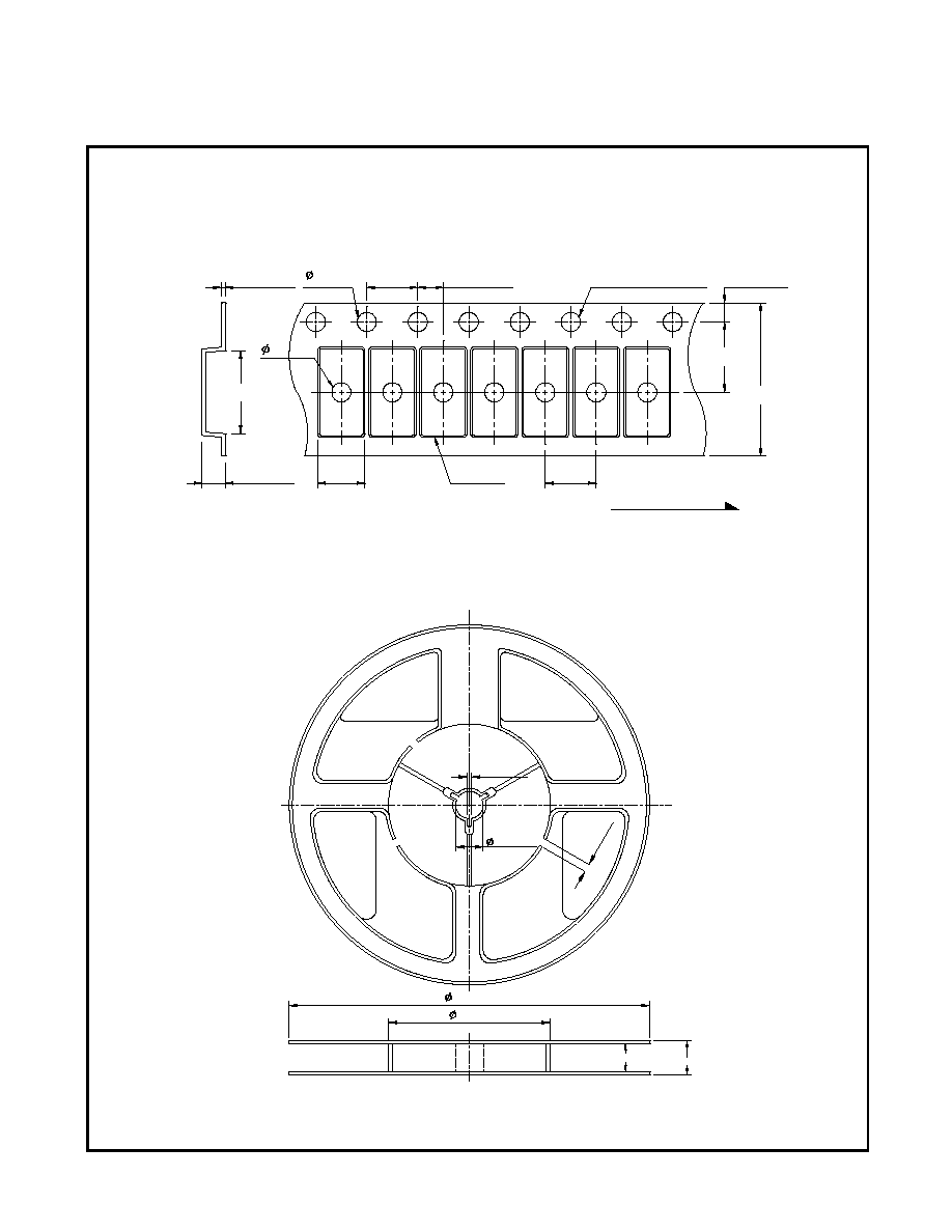
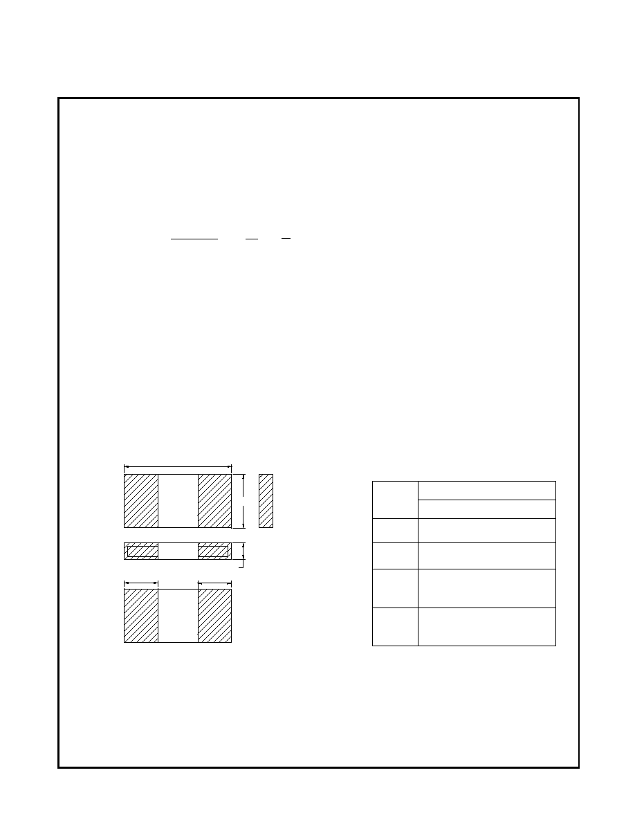
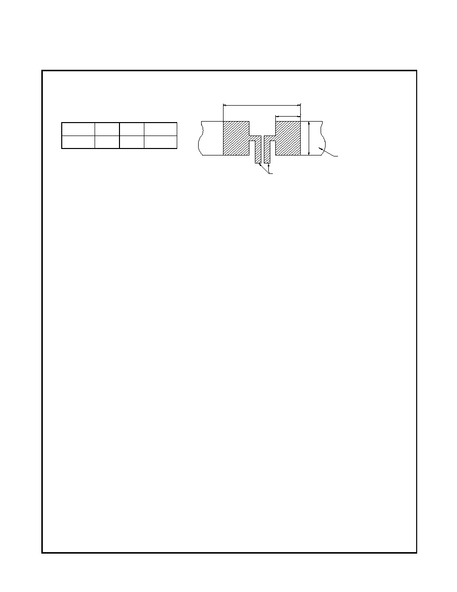
Dimensions and schematic
Figure 1. Construction and Dimensions
a
a
R
0
0
2
L
W
t
Dimensions (mm)
Code
Letter
3264
L
6.35 ± 0.25
W
3.20 ± 0.20
a
(1m) 2.50 ± 0.15
(2m)
1.90 ± 0.15
t
(1m) 0.70 ± 0.15
(2m) 0.65 ± 0.15
CYNTEC CO., LTD.
DOCUMENT : SR960000N
REVISION : A3
PAGE : 2 OF 6
4.
Specification:
Characteristics
Feature
Measurement Method
Power Ratings*
1W
JIS Code 3A/ JIS Code 3D
Resistance Value**
1~2m
Refer to JIS C 5202 5.1
Temperature Coefficient of
Resistance
(1m) ± 200ppm/
(2m) ± 100ppm/
Refer to JIS C 5202 5.2
Operation Temperature Range
-55 ~ +170
Resistance Tolerance
± 1%(F) , ± 2%(G) , ± 5%(J)
JIS C 5201 4.2.4
Insulation Resistance
Over 100M
Refer to JIS C 5202 5.6
Mounting condition G
Maximum Working Voltage (V)
( P*R)
1/2
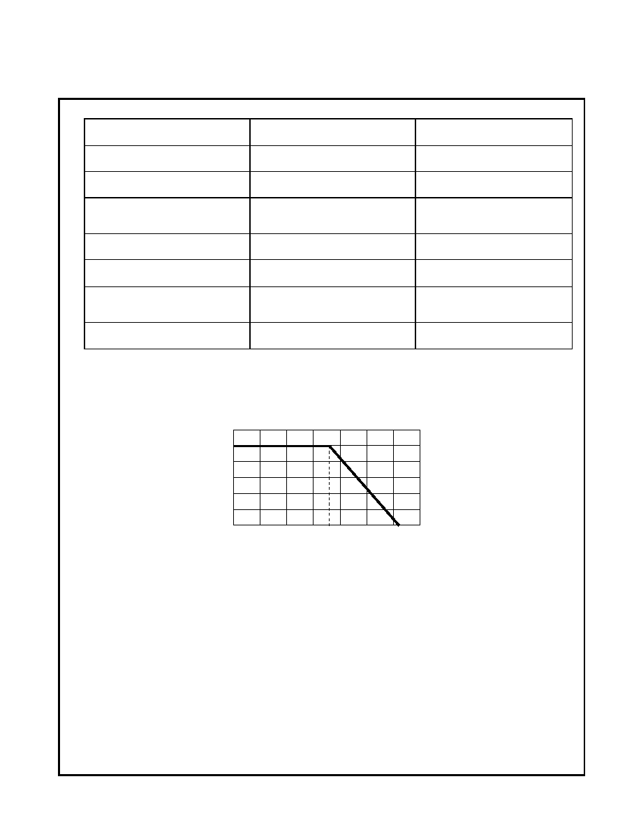
Note * :
Power ratings is based on continuous full load operation at rated ambient temperature of 70. For
resistors operated at ambient temperature in excess of 70, the maximum load shall be derated in
accordance with the following curve.
-55
100
70
0
170
R
A
T
E
D
L
O
A
D
(
%
)
AMBIENT TEMPERATURE()
Figure 2.Power Temperature Derating Cure
CYNTEC CO., LTD.
DOCUMENT : SR960000N
REVISION : A3
PAGE : 3 OF 6
5.
Reliability Performance
Test Item
Condition of Test
Requirements
Short Time Overload
2.5 x Rated power for 5 seconds
Refer to JIS C
5202 5.5
± 0.5%
Thermal Shock
-55 ~150 1,000 cycles, 15 min at each
extreme condition
Refer to JIS C 5202 7.4
± 0.5%
Moisture resistance
MIL-STD-202, Method 106
± 0.5%
Low Temperature Storage
Kept at -55, 1,000 hours
Refer to JIS C 5202 7.1
± 0.5%
Resistance to Soldering Heat Dipped into solder at 270 ± 5
for 20 ± 1 seconds
Refer to JIS C 5202 6.4
± 0.5%
Load Life
Rated voltage for 1.5hours followed by a pause
0.5hour at 70 ± 3
Cycle repeated 1,000 hours
Refer to JIS C 5202 7.10
± 1.0%
Dump Heat with Load
60 ± 2 with relative humidity 90% to 95%.
D.C. rated voltage for 1.5 hours ON
30 minutes OFF.
Cycle repeated 1,000 hours
Refer to JIS C 5202 7.9
± 0.5%
High Temperature Exposure Kept at 170 for 1,000 hours
Refer to JIS C 5202 7.11
± 0.5%
Solderability
Temperature of Solder : 245 ± 5
Immersion Duration : 3 ± 0.5 second
Refer to JIS C 5202 6.5
Uniform coating of solder
cover minimum of 95%
surface being immersed
Mechanical Shock
100 G's for 6milliseconds. 5 pulses
Refer to JIS C 5202 6.2
± 0.5%
Substrate Bending
Glass-Epoxy board thickness : 1.6mm
Bending width : 2mm
Between the fulcrums : 90mm
Refer to JIS C 5202 6.1.4
± 0.5%
CYNTEC CO., LTD.
DOCUMENT : SR960000N
REVISION : A3
PAGE : 4 OF 6
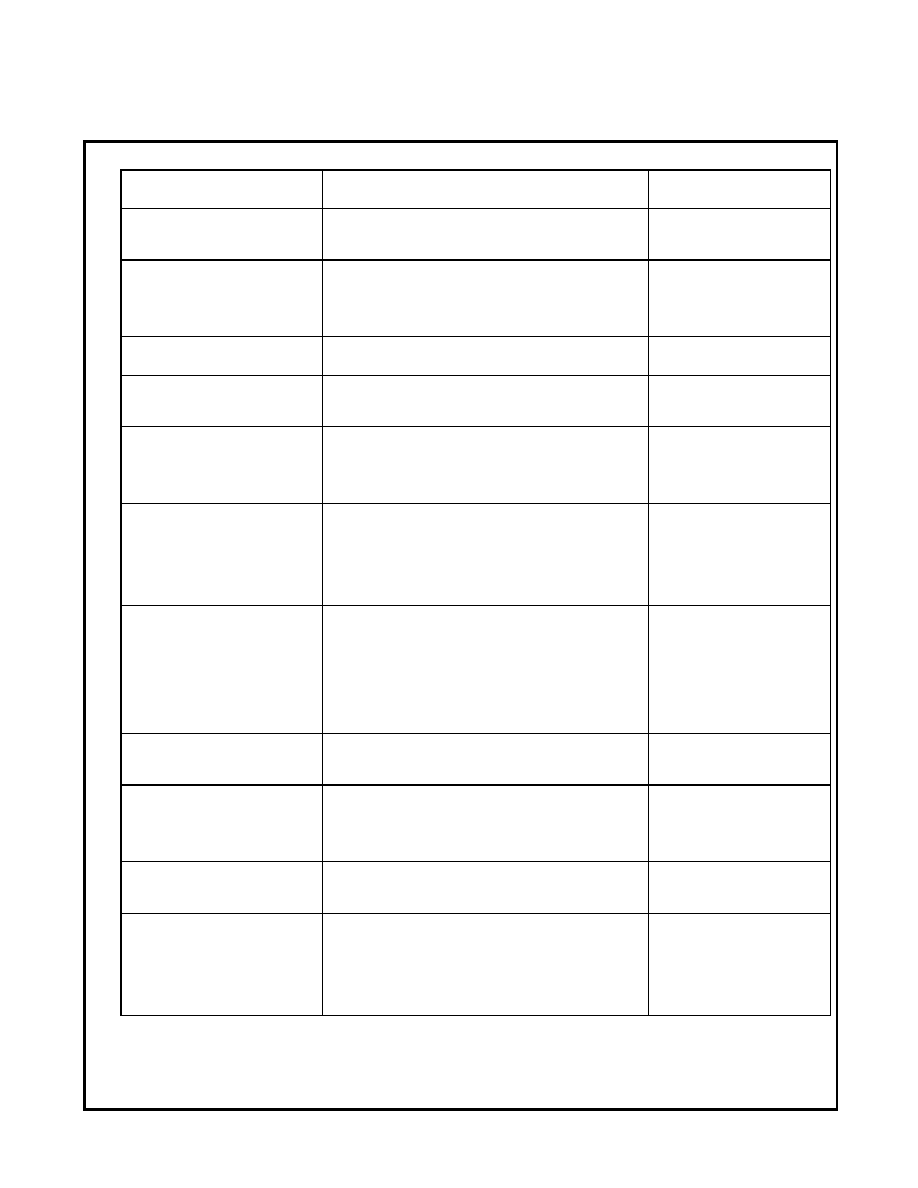
6.
Recommended Solder Pad Dimensions
W
L
D
3264
4.00
8.00
3.35
Note : We recommend there is no circuit design between pads to avoid circuit short
Cu Trace
W
L
D
Sensing Trace