
CYNTEC CO., LTD.
DOCUMENT : RH000001N
REVISION : A1
PAGE : 1 OF9
0402 Series Thick Film Chip Resistor
1.
Scope
This specification applies to 1.0mm x 0.5mm ( 0402 ) size, fixed metal chip resistors rectangular
type for use in electronic equipment.
2.
Type Designation
RR0510
X -- XXX -- X
N
(1)
(2)
(3)
(4) (6)
RR0510
X --
000
-- X
N
(1)
(2)
(3)
(5) (6)
Where
(1)
Series No.
(2)
Tolerance of TCR :
X = Jumper
Resistor refer to paragraph 3
(3)
Nominal resistance value :
For example �-
Three digits of number (E-24 Series)
000 = Jumper0
100 = 10
102 = 1k
Four digits of number (E-96 Series)
11R3 = 11.3
1131 =1.13k
(4)
Resistance tolerance :
D = �0.5%
F = �1.0%
J = �5.0%
(5)
Resistance tolerance :
X = JumperBelow 50m
(6)
N = Sn plating (Lead free, RoHS compliant)

CYNTEC CO., LTD.
DOCUMENT : RH000001N
REVISION : A1
PAGE : 2 OF9
3.
Electrical Specifications
Table 1. :
Power Rating*
1/16 W
Resistance Values
E-24 series , E-96 series
Resistance Tolerance
�
0.1%(B) , � 0.5%(D) , � 1.0%(F)
�
1.0%(F)
�
1.0%(F) , � 5.0%(J)
Resistance Range ( )
10 ~ 97.6
100 ~ 1M
1.02M ~ 10M
1.0 ~ 9.76
10 ~ 10M
Temperature Coefficient
of Resistance
ppm/ (code)
�
100
(R)
�
50
(Q)
�
100
(R)
0 ~ 500
(S)
�
200
(S)
Operating Temperature Range
-55 to +125
Max. Operating Voltage**
50V
Note: *Package Power Temperature Derating Curve
Figure 1.Power Temperature Derating Cure
Note: **Resistors shall have a rated DC or AC(rms.) continuous operating voltage corresponding to
the power rating, as calculated from the following formula
Where V
: Rated voltage (V)
P
: Rated power (W)
R
P
V
�
=
R
: Nominal resistance ()
If the voltage so obtained exceeds the maximum operating voltage, this maximum voltage shall
be the rated voltage.
Table 2. : Jumper:
Resistance Tolerance
Below 50 m
Rated current
1A
Operating Temperature Range
-55 to 125
R
A
T
E
D
L
O
A
D
(
%
)
AMBIENT TEMPERATURE(
)
0
-55
70
125
100
CYNTEC CO., LTD.
DOCUMENT : RH000001N
REVISION : A1
PAGE : 3 OF9
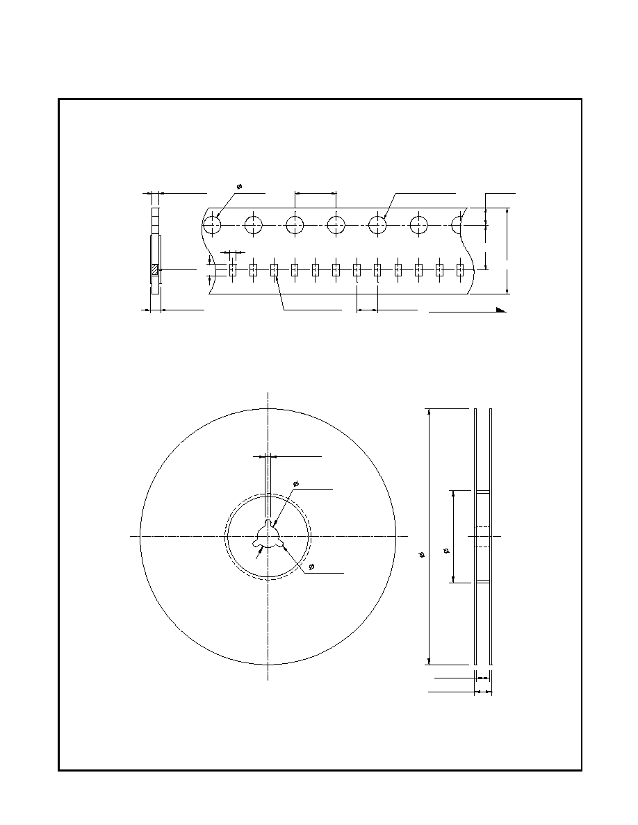
4.
Outline dimensions
5.
Life Tests
5-1 Electrical
Specification and Requirement
Item
Resistor
Jumper
Test Method
Short Time Overload
TCR 100ppm
R: �(1%+ 0.05)
TCR > 100ppm
R: �(2%+ 0.1)
Without damage by
flashover, spark, arcing,
burning or breakdown
Max. 50m
(1)
Applied voltage :
2.5 x rated voltage or
2 x maximum operating voltage
which ever is less
(2)
Test time : 5 seconds
Insulation Resistance Over 100 M on Overcoat layer face up
Over 1,000 M on Substrate side face up
(1)
Setup as figure 2
(2)
Test voltage : 50V
DC
(3)
Test time :
60 + 10 / -0 seconds
Voltage Proof
R:
�
(2%+ 0.1)
Without damage by
flashover, spark, arcing,
burning or breakdown
Max. 50m
(1)
Setup as figure 2
(2)
Test voltage : 100V
AC
(rms.)
(3)
Test time :
60 +10 / -0 seconds
Code Letter
Dimension
L
1.0
�
0.05
W
0.50
�
0.05
t
0.35
�
0.05
a
0.2
�
0.10
Unit : mm
L
W
a
a
t
Insulation Plate
Spring
Sample Electrode
Metal Block
Measurement Point B
Pressure Rod
(Metal)
Measurement Point A
Substrate
Over coat Film
Figure 2 : Measurement Setup
(R=0.5 mm)
A
B
Voltage Supply
Substrate Side
CYNTEC CO., LTD.
DOCUMENT : RH000001N
REVISION : A1
PAGE : 4 OF9
5-2 Mechanical
Specification and Requirement
Item
Resistor
Jumper
Test Method
Solderability
The surface of terminal immersed shall be
minimum of 95% covered with a new
coating of solder
Solder bath :
After immersing in flux, dip in
245
�
5 molten solder bath
for 2
�
0.5 seconds
Resistance to Solder
Heat
R:
�
(1.0%+ 0.05)
Without distinct
deformation in
appearance
Max. 50m
(1)
Pre-heat: 100~110 for
30 seconds
(2)
Immersed at solder bath
of 270
�
5 for
10
�
1 seconds
(3)
Measuring resistance
1 hour after test
Vibration
R:
�
(0.5%+ 0.05)
Without mechanical damage such as break
(1)
Vibration frequency :
10Hz to 55Hz to10Hz in 60
seconds as a period
(2)
Vibration time : period cycled
for 2 hours in each of 3 mutual
perpendicular directions
(3)
Amplitude : 1.5mm
Shock
R:
�
(0.25%+ 0.05)
Without mechanical damage such as break
(1)
Peak value : 490N
(2)
Duration of pulse : 11ms
(3)
3 times in each positive and
negative direction of 3 mutual
perpendicular
directions
Bending Test
R: �(1.0%+ 0.05)
Without mechanical
damage such as break
Max. 50m
Bending value : 3 mm for
30
�
1 seconds
CYNTEC CO., LTD.
DOCUMENT : RH000001N
REVISION : A1
PAGE : 5 OF9
5-3 Endurance
Specification and Requirement
Item
Resistor
Jumper
Test Method
Rapid change of
Temperature
R: �(1.0%+ 0.05)
Without distinct damage in
appearance
Max. 50m
(1)
Repeat 5 cycle as follows :
(-55
�
3,30minutes) (Room
temperature, 2~3 minutes)
(+125
�
2,30minutes)
(Room temperature, 2~3
minutes)
(2)
Measuring resistance
1 hour after test
Moisture with Load R: �(5.0%+ 0.1)
Without distinct damage
in appearance
Marking should be
legible
Max. 50m
(1)
Environment condition :
40
�
2,90~95% RH
(4)
Applied Voltage:
rated voltage
(2)
Test period: (1.5 hour ON
(0.5 hour OFF) cycled for
total 1,000 + 48 / - 0 hours
(3)
Measuring resistance
1 hour after test
Load Life
R: �(5.0%+ 0.1)
Without distinct damage
in appearance
Max. 100m
(1)
Test temperature :
70
�
2
(2)
Applied Voltage:
rated voltage
(3)
Test period : (1.5 hour ON)
(0.5 hour OFF) cycled for
total 1,000 + 48 / - 0 hours
(4)
Measuring resistance
1 hour after test
Low Temperature
Store
R: �(5.0%+ 0.1)
Without distinct damage
in appearance
Max. 100m
(1)
Store temperature :
-55
�
3 for total
1,000 + 48 / - 0 hours
(2)
Measuring resistance
1 hour after test
High Temperature
Store
R: �(5.0%+ 0.1)
Without distinct damage
in appearance
Max. 100m
(1)
Store temperature :
+125
�
2 for total
1,000 + 48 / - 0 hours
(2)
Measuring resistance
1 hour after test
CYNTEC CO., LTD.
DOCUMENT : RH000001N
REVISION : A1
PAGE : 6 OF9
6.
Recommend Land Pattern Dimensions
A
0.5
B
1.5
C
0.4~0.8
Unit : mm
C
A
B
CYNTEC CO., LTD.
DOCUMENT : RH000001N
REVISION : A1
PAGE : 7 OF9
7.
Packaging
7-1
Dimensions
7-1-1
Tape packaging dimensions
7-1-2
Reel dimensions
0.1
^ 0.0
B = 1.15 � 0.10
A = 0.65 � 0.10
0.50 � 0.1
Chip
B
A
0.43 � 0.05
1.5
1.75 �0.1
8.0 � 0.3
Unit : mm
3.5 � 0.05
2.0 � 0.05
Carrier cavity
Pull Direction
4.0 � 0.1
Sprocket hole
2.0�0.5
9.0 � 0.3
11.4 � 1.0
Unit : mm
1
7
8
�
2
.
0
6
0
�
2
.
0
21 � 0.8
13 � 0.2

CYNTEC CO., LTD.
DOCUMENT : RH000001N
REVISION : A1
PAGE : 8 OF9
7-2
Peel force of top cover tape
The peel speed shall be about 300 mm/minute
The peel force of top cover tape shall be between 0.1 to 0.7 N
7-3
Numbers of taping
10,000 pieces/reel
7-4 Label marking
The following items shall be marked on the production and shipping
Label on the reel.
7-4-1
Production Label
(1)
Part No.
(2)
Description
(3)
Quantity
(4)
Taping No.
7-4-2
Shipping Label
(1)
*Customer's name
(2)
*Customer's part No.
(3)
Manufacturer's part No.
(4)
Manufacturer's name
(5)
Manufacturer's country
*Note : Item (1) and (2) are listed by request
165 ~ 180�
Top Cover Tape
0.1~0.7 N

CYNTEC CO., LTD.
DOCUMENT : RH000001N
REVISION : A1
PAGE : 9 OF9
8.
Care note
8-1
Care note for storage
(1)
Chip resistor shall be stored in a room where temperature and humidity must be controlled.
(temperature 5 to 35, humidity 45 to 85% RH) However, a humidity keep it low, as it is
possible.
(2)
Chip resistor shall be stored as direct sunshine doesn't hit on it.
(3)
Chip resistor shall be stored with no moisture, dust, a material that will make solderability
inferior, and a harmful gas (Chloridation hydrogen, sulfurous acid gas, and sulfuration
hydrogen)
8-2
Care note for operating and handling
(1)
It is necessary to protect the edge and protection coat of resistors from mechanical stress.
(2)
Handle with care when printing circuit board (PCB) is divided or fixed on support body,
because bending of printing circuit board (PCB) mounting will make mechanical stress for
resistors.
(3)
Resistors shall be used with in rated range shown in specification. Especially, if voltage more
than specified value will be loaded to resistor, there is a case it will make damage for
machine because of temperature rise depending on generating of heat, and increase
resistance value or breaks.
(4)
In case that resistor is loaded a rated voltage, it is necessary to confirms temperature of a
resistor and to reduce a load power according to load reduction curve, because a temperature
rise of a resistor depends on influence of heat from mounting density and neighboring
element.
(5)
Observe Limiting element voltage and maximum overload voltage specified in each
specification
(6)
If there is possibility that a large voltage (pulse voltage, shock voltage) charge to resistor, it
is necessary that operating condition shall be set up before use.