 | –≠–ª–µ–∫—Ç—Ä–æ–Ω–Ω—ã–π –∫–æ–º–ø–æ–Ω–µ–Ω—Ç: 20V8 | –°–∫–∞—á–∞—Ç—å:  PDF PDF  ZIP ZIP |
Flash Erasable,
Reprogrammable CMOS PAL
Device
PALCE20V8
Cypress Semiconductor Corporation
∑
3901 North First Street
∑
San Jose
∑
CA 95134
∑
408-943-2600
Document #: 38-03026 Rev. **
Revised March 26, 1997
20V8
Features
∑ Active pull-up on data input pins
∑ Low power version (20V8L)
-- 55 mA max. commercial (15, 25 ns)
-- 65 mA max. military/industrial
(15, 25 ns)
∑ Standard version has low power
-- 90 mA max. commercial
(15, 25 ns)
-- 115 mA max. commercial (10 ns)
-- 130 mA max. military/industrial (15, 25 ns)
∑ CMOS Flash technology for electrical erasability and
reprogrammability
∑ User-programmable macrocell
-- Output polarity control
-- Individually selectable for registered or combinato-
rial operation
∑ QSOP package available
-- 10, 15, and 25 ns com'l version
-- 15, and 25 ns military/industrial versions
∑ High reliability
-- Proven Flash technology
-- 100% programming and functional testing
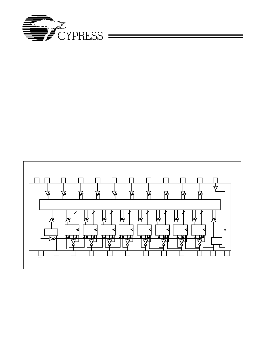
Functional Description
The Cypress PALCE20V8 is a CMOS Flash Erasable sec-
ond-generation programmable array logic device. It is imple-
mented with the familiar sum-of-product (AND-OR) logic struc-
ture and the programmable macrocell.
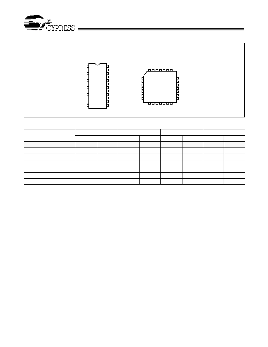
The PALCE20V8 is executed in a 24-pin 300-mil molded DIP,
a 300-mil cerdip, a 28-lead square ceramic leadless chip car-
rier, a 28-lead square plastic leaded chip carrier, and a 24-lead
quarter size outline. The device provides up to 20 inputs and
8 outputs. The PALCE20V8 can be electrically erased and re-
programmed. The programmable macrocell enables the de-
vice to function as a superset to the familiar 24-pin PLDs such
as 20L8, 20R8, 20R6, 20R4.
PAL is a registered trademark of Advanced Micro Devices, Inc.
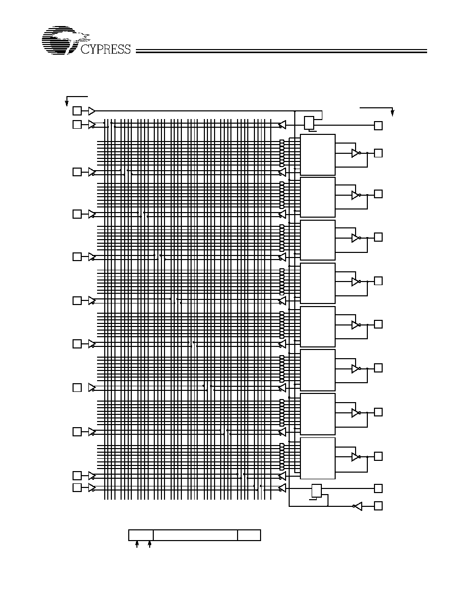
Logic Block Diagram (PDIP/CDIP/QSOP)
20V8≠1
8
8
8
8
8
8
8
8
10
9
8
7
6
5
4
3
2
1
13
15
16
17
18
19
20
21
22
23
PROGRAMMABLE
AND ARRAY
(64 x 40)
Macrocell
Macrocell
Macrocell
Macrocell
Macrocell
Macrocell
Macrocell
Macrocell
I
9
I
8
I
7
I
6
I
5
I
4
I
3
I
2
I
1
CLK/I
0
OE/I
11
I/O
0
I/O
1
I/O
2
I/O
3
I/O
4
I/O
5
I/O
6
I/O
7
I
13
12
GND
11
I
10
MUX
24
V
CC
MUX
14
I
12
PALCE20V8
Document #: 38-03026 Rev. **
Page 2 of 14
Shaded area contains preliminary information.
Functional Description
(continued)
The PALCE20V8 features 8 product terms per output and 40
input terms into the AND array. The first product term in a mac-
rocell can be used either as an internal output enable control
or as a data product term.
There are a total of 18 architecture bits in the PALCE20V8
macrocell; two are global bits that apply to all macrocells and
16 that apply locally, two bits per macrocell. The architecture
bits determine whether the macrocell functions as a register or
combinatorial with inverting or noninverting output. The output
enable control can come from an external pin or internally from
a product term. The output can also be permanently enabled,
functioning as a dedicated output or permanently disabled,
functioning as a dedicated input. Feedback paths are select-
able from either the input/output pin associated with the mac-
rocell, the input/output pin associated with an adjacent pin, or
from the macrocell register itself.
Power-Up Reset
All registers in the PALCE20V8 power-up to a logic LOW for
predictable system initialization. For each register, the associ-
ated output pin will be HIGH due to active-LOW outputs.
Electronic Signature
An electronic signature word is provided in the PALCE20V8
that consists of 64 bits of programmable memory that can con-
tain user-defined data.
Security Bit
A security bit is provided that defeats the readback of the in-
ternal programmed pattern when the bit is programmed.
Low Power
The Cypress PALCE20V8 provides low-power operation
through the use of CMOS technology, and increased testability
with Flash reprogrammability.
Product Term Disable
Product Term Disable (PTD) fuses are included for each prod-
uct term. The PTD fuses allow each product term to be individ-
ually disabled.
Input and I/O Pin Pull-Ups
The PALCE20V8 input and I/O pins have built-in active
pull-ups that will float unused inputs and I/Os to an active
HIGH state (logical 1). All unused inputs and three-stated I/O
pins should be connected to another active input, V
CC
, or
Ground to improve noise immunity and reduce I
CC
.
Pin Configuration
PLCC/LCC
Top View
20V8≠2
DIP/QSOP
Top View
25
24
23
22
21
20
19
5
6
7
8
9
10
11
121314 1516 1718
4 3 2
2827 26
I
I
CL
K
/
I
V
I
I/
O
13
7
CC
1
NC
1
2
3
4
5
6
7
8
9
10
11
14
15
16
20
19
18
17
21
24
23
22
12
13
OE/I
11
I/O
7
I/O
0
I/O
2
I/O
1
I/O
6
I/O
5
I
12
I/O
3
V
CC
I/O
4
GND
I
1
CLK/I
0
I
13
20V8≠3
I
2
I
3
I
4
I
5
I
6
I
7
I
8
I
9
I
10
0
1
2
I
3
I
4
I
5
I
6
I
7
I
8
NC
I/O
2
I/O
1
I/O
6
I/O
5
I/O
3
I/O
4
NC
10
9I
I
GND
NC
11
12
0
OE
/I
I
I/O
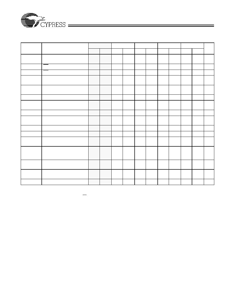
Selection Guide
Generic Part Number
t
PD
ns
t
S
ns
t
CO
ns
I
CC
mA
Com'l/Ind
Mil
Com'l/Ind
Mil
Com'l/Ind
Mil
Com'l
Mil/Ind
PALCE20V8
-
5
5
3
4
115
PALCE20V8
-
7
7.5
7
5
115
PALCE20V8
-
10
10
10
10
10
7
10
115
130
PALCE20V8
-
15
15
15
12
12
10
12
90
130
PALCE20V8
-
25
25
25
15
20
12
20
90
130
PALCE20V8L
-
15
15
15
12
12
10
12
55
65
PALCE20V8L
-
25
25
25
15
20
12
20
55
65

PALCE20V8
Document #: 38-03026 Rev. **
Page 3 of 14
Maximum Ratings
(Above which the useful life may be impaired. For user guide-
lines, not tested.)
Storage Temperature
..................................... -
65
∞
C to +150
∞
C
Ambient Temperature with
Power Applied
.................................................. -
55
∞
C to +125
∞
C
Supply Voltage to Ground Potential
(Pin 24 to Pin 12)
.................................................-
0.5V to +7.0V
DC Voltage Applied to Outputs
in High Z State
.....................................................-
0.5V to +7.0V
DC Input Voltage
.................................................-
0.5V to +7.0V
Output Current into Outputs (LOW)............................. 24 mA
DC Programming Voltage............................................. 12.5V
Latch-Up Current ..................................................... >200 mA
Configuration Table
CG
0
CG
1
CL0
x
Cell Configuration
Devices Emulated
0
1
0
Registered Output
Registered Med PALs
0
1
1
Combinatorial I/O
Registered Med PALs
1
0
0
Combinatorial Output
Small PALs
1
0
1
Input
Small PALs
1
1
1
Combinatorial I/O
20L8 only
Macrocell
Q
Q
D
CLK
20V8≠4
1
1
0
0
1
X
CL1
x
0
1
X
0
1 1
I/O
x
From
Adjacent
Pin
CL0
x
CG
1
for pin 16 to 21 (DIP)
CG
0
for pin 15 and 22 (DIP)
1
0
0
1
1 1
0 0
0
1
X
0
1 1
OE
V
CC
To
Adjacent
Macrocell
CL0
x
CG
1
V
CC
Operating Range
Range
Ambient
Temperature
V
CC
Commercial
0
∞
C to +75
∞
C
5V
±
5%
Industrial
-
40
∞
C to +85
∞
C
5V
±
10%
Military
[1]
-
55
∞
C to +125
∞
C
5V
±
10%
Note:
1.
T
A
is the "instant on" case temperature.
PALCE20V8
Document #: 38-03026 Rev. **
Page 4 of 14
Electrical Characteristics
Over the Operating Range
[2]
Parameter
Description
Test Conditions
Min.
Max.
Unit
V
OH
Output HIGH Voltage
V
CC
= Min.,
V
IN
= V
IH
or V
IL
I
OH
=
-
3.2 mA
Com'l
2.4
V
I
OH
=
-
2 mA
Mil/Ind
V
OL
Output LOW Voltage
V
CC
= Min.,
V
IN
= V
IH
or V
IL
I
OL
= 24 mA
Com'l
0.5
V
I
OL
= 12 mA
Mil/Ind
V
IH
Input HIGH Level
Guaranteed Input Logical HIGH Voltage for All Inputs
[3]
2.0
V
V
IL
[4]
Input LOW Level
Guaranteed Input Logical LOW Voltage for All Inputs
[3]
-
0.5
0.8
V
I
IH
Input or I/O HIGH Leakage
Current
3.5V < V
IN
< V
CC
10
µ
A
I
IL
[5]
Input or I/O LOW Leakage
Current
0V < V
IN
< V
IN
(Max.)
-
100
µ
A
I
SC
Output Short Circuit Current V
CC
= Max., V
OUT
= 0.5V
[6,7]
-
30
-
150
mA
I
CC
Operating Power Supply
Current
V
CC
= Max.,
V
IL
= 0V, V
IH
= 3V,
Output Open,
f = 15 MHz
(counter)
5, 7, 10 ns
Com'l
115
mA
15, 25 ns
90
mA
15L, 25L ns
55
mA
10, 15, 25 ns
Mil/Ind
130
mA
15L, 25L ns
Mil/Ind
65
mA
Capacitance
[7]
Parameter
Description
Test Conditions
Typ.
Unit
C
IN
Input Capacitance
V
IN
= 2.0V @ f = 1 MHz
5
pF
C
OUT
Output Capacitance
V
OUT
= 2.0V @ f = 1 MHz
5
pF
Endurance Characteristics
[7]
Parameter
Description
Test Conditions
Min.
Max.
Unit
N
Minimum Reprogramming Cycles
Normal Programming Conditions
100
Cycles
Notes:
2.
See the last page of this specification for Group A subgroup testing information.
3.
These are absolute values with respect to device ground. All overshoots due to system or tester noise are included.
4.
V
IL
(Min.) is equal to
-
3.0V for pulse durations less than 20 ns.
5.
The leakage current is due to the internal pull-up resistor on all pins.
6.
Not more than one output should be tested at a time. Duration of the short circuit should not be more than one second. V
OUT
= 0.5V has been chosen to avoid test problems
caused by tester ground degradation.
7.
Tested initially and after any design or process changes that may affect these parameters.
PALCE20V8
Document #: 38-03026 Rev. **
Page 5 of 14
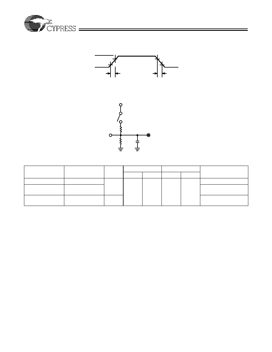
AC Test Loads and Waveforms
90%
10%
3.0V
GND
90%
10%
ALL INPUT PULSES
2 ns
2 ns
20V8≠5
OUTPUT
R2
R1
C
L
S1
5V
TEST POINT
20V8≠6
Specification
S
1
C
L
Commercial
Military
Measured Output Value
R
1
R
2
R
1
R
2
t
PD
, t
CO
Closed
50 pF
200
390
390
750
1.5V
t
PZX
, t
EA
Z
H: Open
Z
L: Closed
1.5V
t
PXZ
, t
ER
H
Z: Open
L
Z: Closed
5 pF
H
Z: V
OH
-
0.5V
L
Z: V
OL
+ 0.5V
PALCE20V8
Document #: 38-03026 Rev. **
Page 6 of 14
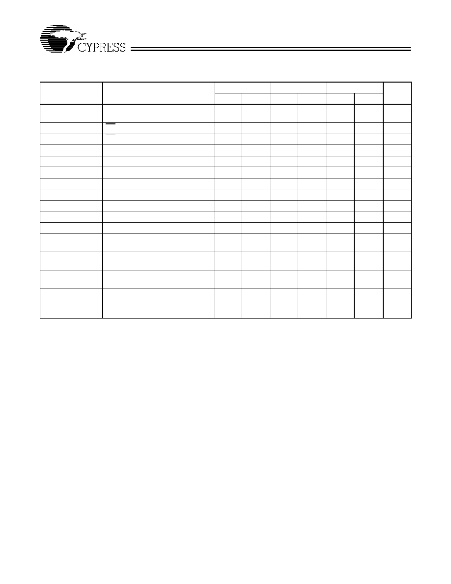
Commercial and Industrial Switching Characteristics
[2]
20V8
-
5
20V8
-
7
20V8
-
10
20V8
-
15
20V8
-
25
Parameter
Description
Min.
Max.
Min.
Max.
Min.
Max.
Min.
Max.
Min.
Max.
Unit
t
PD
Input to Output
Propagation Delay
[8]
1
5
1
7.5
1
10
1
15
1
25
ns
t
PZX
OE to Output Enable
5
6
10
15
20
ns
t
PXZ
OE to Output Disable
5
6
10
15
20
ns
t
EA
Input to Output
Enable Delay
[7]
6
9
10
15
25
ns
t
ER
Input to Output
Disable Delay
[7,9]
6
9
10
15
25
ns
t
CO
Clock to Output Delay
[8]
1
4
1
5
1
7
1
10
1
12
ns
t
S
Input or Feedback
Set-Up Time
3
7
10
12
15
ns
t
H
Input Hold Time
0
0
0
0
0
ns
t
P
External Clock Period
(t
CO
+ t
S
)
7
12
17
22
27
ns
t
WH
Clock Width HIGH
[7]
3
5
8
8
12
ns
t
WL
Clock Width LOW
[7]
3
5
8
8
12
ns
f
MAX1
External Maximum
Frequency (1/(t
CO
+ t
S
))
[7,10]
143
83
58
45.5
37
MHz
f
MAX2
Data Path Maximum
Frequency
(1/(t
WH
+ t
WL
))
[7, 11]
166.
6
100
62.5
62.5
41.6
MHz
f
MAX3
Internal Feedback Maximum
Frequency (1/(t
CF
+ t
S
))
[7,12]
166.
6
100
62.5
50
40
MHz
t
CF
Register Clock to
Feedback Input
[7, 13]
3
3
6
8
10
ns
t
PR
Power-Up Reset Time
[7]
1
1
1
1
1
µ
s
Shaded area contains preliminary information.
Notes:
8.
Min. times are tested initially and after any design or process changes that may affect these parameters.
9.
This parameter is measured as the time after OE pin or internal disable input disables or enables the output pin. This delay is measured to the point at which a previous
HIGH level has fallen to 0.5 volts below V
OH
min. or a previous LOW level has risen to 0.5 volts above V
OL
max.
10. This specification indicates the guaranteed maximum frequency at which a state machine configuration with external feedback can operate.
11.
This specification indicates the guaranteed maximum frequency at which the device can operate in data path mode.
12. This specification indicates the guaranteed maximum frequency at which a state machine configuration with internal only feedback can operate.
13. This parameter is calculated from the clock period at f
MAX
internal (1/f
MAX3
) as measured (see Note 7 above) minus t
S
.
PALCE20V8
Document #: 38-03026 Rev. **
Page 7 of 14
Shaded area contains preliminary information.
Military Switching Characteristics
[2]
Parameter
Description
20V8
-
10
20V8
-
15
20V8
-
25
Min.
Max.
Min.
Max.
Min.
Max.
Unit
t
PD
Input to Output
Propagation Delay
[8]
1
10
1
15
1
25
ns
t
PZX
OE to Output Enable
10
15
20
ns
t
PXZ
OE to Output Disable
10
15
20
ns
t
EA
Input to Output Enable Delay
[7]
10
15
25
ns
t
ER
Input to Output Disable Delay
[7,9]
10
15
25
ns
t
CO
Clock to Output Delay
[8]
1
10
1
12
1
20
ns
t
S
Input or Feedback Set-Up Time
10
12
20
ns
t
H
Input Hold Time
0
0
0
ns
t
P
External Clock Period (t
CO
+ t
S
)
20
24
40
ns
t
WH
Clock Width HIGH
[7]
8
10
15
ns
t
WL
Clock Width LOW
[7]
8
10
15
ns
f
MAX1
External Maximum Frequency
(1/(t
CO
+ t
S
)
[7,10]
50
41.7
25
MHz
f
MAX2
Data Path Maximum Frequency
(1/(t
WH
+ t
WL
))
[7, 11 ]
62.5
50
33.3
MHz
f
MAX3
Internal Feedback Maximum
Frequency (1/(t
CF
+ t
S
))
[7,12]
62.5
50
33.3
MHz
t
CF
Register Clock to
Feedback Input
[7, 13]
6
8
10
ns
t
PR
Power-Up Reset Time
[7]
1
1
1
µ
s
PALCE20V8
Document #: 38-03026 Rev. **
Page 8 of 14
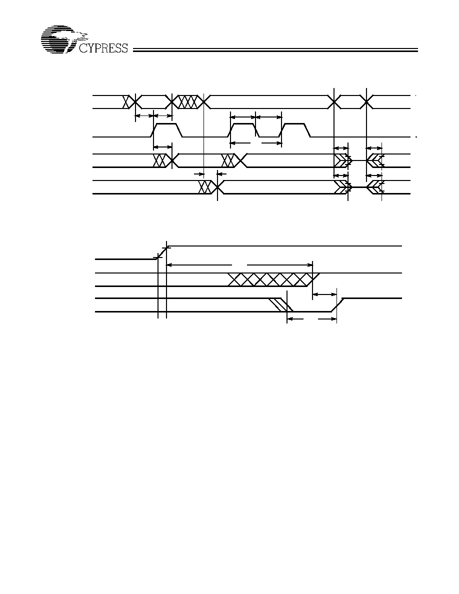
Switching Waveform
t
S
t
H
t
WL
t
WH
t
P
t
CO
t
PD
20V8≠7
t
PXZ
, t
ER
INPUTS, I/O,
REGISTERED
FEEDBACK
CP
REGISTERED
OUTPUTS
COMBINATORIAL
OUTPUTS
t
PXZ
, t
ER
t
EA
, t
PZX
t
EA
, t
PZX
[10]
[10]
[10]
[10]
Power-Up Reset Waveform
t
PR
POWER
CLOCK
t
S
t
WL
10%
REGISTERED
ACTIVE LOW
OUTPUTS
20V8≠8
SUPPLY VOLTAGE
t
PR
MAX = 1
µ
s
90%
V
CC
PALCE20V8
Document #: 38-03026 Rev. **
Page 9 of 14
Functional Logic Diagram for PALCE20V8
0
1 (2)
16
20
24
28
0
12
8
4
3 (4)
22 (26)
13 (16)
20V8≠9
MC7
CL1=2560
CL0=2632
4 (5)
21 (25)
MC6
CL1=2561
CL0=2633
5 (6)
20 (24)
MC5
CL1=2562
CL0=2634
6 (7)
19 (23)
MC4
CL1=2563
CL0=2635
7 (9)
18 (21)
MC3
CL1=2564
CL0=2636
8 (10)
17 (20)
MC2
CL1=2565
CL0=2637
9 (11)
16 (19)
MC1
CL1=2566
CL0=2638
10 (12)
15 (18)
MC0
CL1=2567
CL0=2639
ELECTRONIC SIGNATURE ROW
BYTE7
BYTE6 . . .
. . . BYTE1
BYTE0
2568
2569 . . .
. . . 2630
2631
MSB LSB
CG
0
=2704
CG
1
=2705
23 (27)
PIN NUMBERS DIP (PLCC) PACKAGE
280
320
640
960
1280
1600
1920
2240
32
32
PTD
2 (3)
1
0
CG
0
11 (13)
600
14 (17)
0
1
CG
0
PIN NUMBERS DIP (PLCC)PACKAGE
920
1240
1560
1880
2200
2520
PALCE20V8
Document #: 38-03026 Rev. **
Page 10 of 14
Shaded area contains preliminary information.
Ordering Information for PALCE20V8
I
CC
(mA)
t
PD
(ns)
t
S
(ns)
t
CO
(ns)
Ordering Code
Package
Name
Package Type
Operating
Range
115
5
3
4
PALCE20V8
-
5JC
J64
28-Lead Plastic Leaded Chip Carrier
Commercial
115
7.5
7
5
PALCE20V8
-
7JC
J64
28-Lead Plastic Leaded Chip Carrier
Commercial
PALCE20V8
-
7PC
P13
24-Lead (300-Mil) Molded DIP
115
10
10
7
PALCE20V8
-
10JC
J64
28-Lead Plastic Leaded Chip Carrier
PALCE20V8
-
10PC
P13
24-Lead (300-Mil) Molded DIP
PALCE20V8
-
10QC
Q13
24-Lead Quarter-Size Outline
130
10
10
10
PALCE20V8
-
10JI
J64
28-Lead Plastic Leaded Chip Carrier
Industrial
PALCE20V8
-
10PI
P13
24-Lead (300-Mil) Molded DIP
PALCE20V8
-
10DMB
D14
24-Lead (300-Mil) CerDIP
Military
PALCE20V8
-
10LMB
L64
28-Pin Square Leadless Chip Carrier
90
15
12
10
PALCE20V8
-
15JC
J64
28-Lead Plastic Leaded Chip Carrier
Commercial
PALCE20V8
-
15PC
P13
24-Lead (300-Mil) Molded DIP
PALCE20V8
-
15QC
Q13
24-Lead Quarter-Size Outline
130
15
12
12
PALCE20V8
-
15JI
J64
28-Lead Plastic Leaded Chip Carrier
Industrial
PALCE20V8
-
15PI
P13
24-Lead (300-Mil) Molded DIP
PALCE20V8
-
15QI
Q13
24-Lead Quarter-Size Outline
PALCE20V8
-
15DMB
D14
24-Lead (300-Mil) CerDIP
Military
PALCE20V8
-
15LMB
L64
28-Pin Square Leadless Chip Carrier
90
25
15
12
PALCE20V8
-
25JC
J64
28-Lead Plastic Leaded Chip Carrier
Commercial
PALCE20V8
-
25PC
P13
24-Lead (300-Mil) Molded DIP
PALCE20V8
-
25QC
Q13
24-Lead Quarter-Size Outline
130
25
20
20
PALCE20V8
-
25JI
J64
28-Lead Plastic Leaded Chip Carrier
Industrial
PALCE20V8
-
25PI
P13
24-Lead (300-Mil) Molded DIP
PALCE20V8
-
25QI
Q13
24-Lead Quarter-Size Outline
PALCE20V8
-
25DMB
D14
24-Lead (300-Mil) CerDIP
Military
PALCE20V8
-
25LMB
L64
28-Pin Square Leadless Chip Carrier
PALCE20V8
Document #: 38-03026 Rev. **
Page 11 of 14
MILITARY SPECIFICATIONS
Group A Subgroup Testing
Ordering Information for PALCE20V8L
I
CC
(mA)
t
PD
(ns)
t
S
(ns)
t
CO
(ns)
Ordering Code
Package
Name
Package Type
Operating
Range
55
15
12
10
PALCE20V8L
-
15JC
J64
28-Lead Plastic Leaded Chip Carrier
Commercial
PALCE20V8L
-
15PC
P13
24-Lead (300-Mil) Molded DIP
PALCE20V8L
-
15QC
Q13
24-Lead Quarter-Size Outline
65
15
12
12
PALCE20V8L
-
15JI
J64
28-Lead Plastic Leaded Chip Carrier
Industrial
PALCE20V8L
-
15PI
P13
24-Lead (300-Mil) Molded DIP
PALCE20V8L
-
15QI
Q13
24-Lead Quarter-Size Outline
PALCE20V8L
-
15DMB
D14
24-Lead (300-Mil) CerDIP
Military
PALCE20V8L
-
15LMB
L64
28-Pin Square Leadless Chip Carrier
55
25
15
12
PALCE20V8L
-
25JC
J64
28-Lead Plastic Leaded Chip Carrier
Commercial
PALCE20V8L
-
25PC
P13
24-Lead (300-Mil) Molded DIP
PALCE20V8L
-
25QC
Q13
24-Lead Quarter-Size Outline
65
25
20
20
PALCE20V8L
-
25JI
J64
28-Lead Plastic Leaded Chip Carrier
Industrial
PALCE20V8L
-
25PI
P13
24-Lead (300-Mil) Molded DIP
PALCE20V8L
-
25QI
Q13
24-Lead Quarter-Size Outline
PALCE20V8L
-
25DMB
D14
24-Lead (300-Mil) CerDIP
Military
PALCE20V8L
-
25LMB
L64
28-Pin Square Leadless Chip Carrier
DC Characteristics
Parameter
Subgroups
V
OH
1, 2, 3
V
OL
1, 2, 3
V
IH
1, 2, 3
V
IL
1, 2, 3
I
IX
1, 2, 3
I
OZ
1, 2, 3
I
CC
1, 2, 3
Switching Characteristics
Parameter
Subgroups
t
PD
9, 10, 11
t
CO
9, 10, 11
t
S
9, 10, 11
t
H
9, 10, 11
DC Characteristics
Parameter
Subgroups

PALCE20V8
Document #: 38-03026 Rev. **
Page 12 of 14
Package Diagrams
24-Lead (300-Mil) CerDIP D14
MIL
-
STD
-
1835
D
-
9 Config.A
28-Lead Plastic Leaded Chip Carrier J64
28-Square Leadless Chip Carrier L64
MIL
-
STD
-
1835 C
-
4
PALCE20V8
Document #: 38-03026 Rev. **
Page 13 of 14
© Cypress Semiconductor Corporation, 1997. The information contained herein is subject to change without notice. Cypress Semiconductor Corporation assumes no responsibility for the use
of any circuitry other than circuitry embodied in a Cypress Semiconductor product. Nor does it convey or imply any license under patent or other rights. Cypress Semiconductor does not authorize
its products for use as critical components in life-support systems where a malfunction or failure may reasonably be expected to result in significant injury to the user. The inclusion of Cypress
Semiconductor products in life-support systems application implies that the manufacturer assumes all risk of such use and in doing so indemnifies Cypress Semiconductor against all charges.
Package Diagrams
(continued)
24-Lead (300-Mil) Molded DIP P13/P13A
24-Lead Quarter Size Outline Q13

PALCE20V8
Document #: 38-03026 Rev. **
Page 14 of 14
Document Title: PALCE20V8 Flash Erasable, Reprogrammable CMOS PALÆ Device
Document Number: 38-03026
REV.
ECN NO.
Issue
Date
Orig. of
Change
Description of Change
**
106371
07/11/01
SZV
Change from Spec Number: 38-00367 to 38-03026