 | –≠–ª–µ–∫—Ç—Ä–æ–Ω–Ω—ã–π –∫–æ–º–ø–æ–Ω–µ–Ω—Ç: C9630CY | –°–∫–∞—á–∞—Ç—å:  PDF PDF  ZIP ZIP |
PC133 Clock Generator for SiS630/Pentium
Æ
III & SiS540/Socket7 Applications
Cypress Semiconductor Corporation
525 Los Coches St.
Document#: 38-07035 Rev. **
05/02/2001
Milpitas, CA 95035. Tel: 408-263-6300, Fax: 408-263-6571
Page 1 of 18
http://www.cypress.com
APPROVED PRODUCT
C9630
Product Features
∑
Supports
Pentium
III, K6, and Socket 7 CPU's
∑
Designed to SiS630 & SiS540 Chipset requirements
∑
3 copies of CPU Clock (CPU[0:2] )
∑
14 copies of SDRAM Clock (SDRAM[0:13]
∑
7 copies of PCI Clock
∑
2 REF(0:1) Clock outputs
∑
1 USB Clock (Non SSC), 48MHz
∑
1 programmable SIO (Non SSC), 24/48MHz
∑
133 MHz SDRAM support
∑
Cypress Spread Spectrum for best EMI reduction
∑
SMBus Support with read back capabilities.
∑
Dial-a-FrequencyTM
Feature
∑
48 Pin SSOP package.
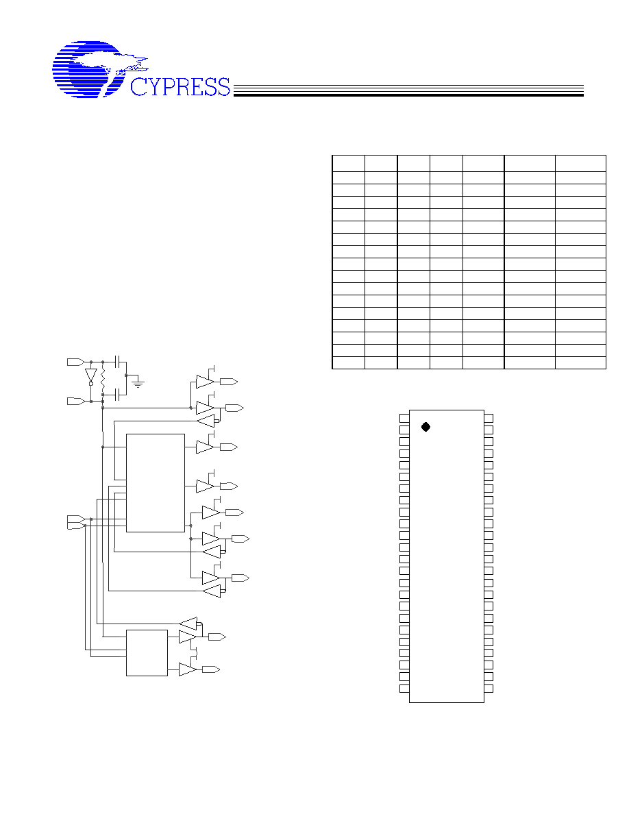
Block Diagram
Fig.1
Frequency Table (MHz)
FS3
FS2
FS1
FS0
CPU
SDRAM
PCICLK
0
0
0
0
66.6
100.0
33.3
0
0
0
1
100.0
100.0
33.3
0
0
1
0
150.0
100.0
37.5
0
0
1
1
133.3
100.0
33.3
0
1
0
0
66.8
133.6
33.4
0
1
0
1
100.0
133.3
33.3
0
1
1
0
100.0
150.0
37.5
0
1
1
1
133.3
133.3
33.3
1
0
0
0
66.9
66.9
33.4
1
0
0
1
97.2
97.2
32.4
1
0
1
0
70.0
105.0
35.0
1
0
1
1
95.0
95.0
31.6
1
1
0
0
95.0
126.7
31.6
1
1
0
1
112.0
112.0
37.3
1
1
1
0
97.0
129.3
32.4
1
1
1
1
96.0
96.0
32.0
Table 1
Note: *Programmable to 48 MHz via SMBus
Pin Configuration
Fig.2
VDD
VDD
VDDcpu
VDD
VDD
VDD
VDD
VDD
VDD
Xin
Xout
REF1
REF0/S3
CPU(0:2)
SDRAM(0:13)
PCI(2:6)
PCI0/S1
PCI1/S2
48MHz/S0
24_48MHz
DATA
SCLK
PLL1
Rin
s1
s0
sdata
sclk
cpu
sdram
pci
s3
s2
PLL2
Rin
48
i2c-clk
i2c-data
24 or 48
1
1
30pF
300K
30pF
3
14
5
1
1
1
1
VDD
S3 / REF0
VSS
XIN
XOUT
VDD
S1/ PCI0
S2 / PCI1
PCI2
VSS
PCI3
PCI4
PCI5
PCI6
VDD
VSS
SDRAM0
SDRAM1
VDD
SDRAM2
SDRAM3
VSS
SDATA
SCLK
REF1
VDDC
CPU0
CPU1
VSS
CPU2
VDD
SDRAM13
SDRAM12
VSS
SDRAM11
SDRAM10
VDD
SDRAM9
SDRAM8
VSS
SDRAM7
SDRAM6
VDD
SDRAM5
SDRAM4
VDD
S0 / 48MHz
24_48MHz
1
2
3
4
5
6
7
8
9
10
11
12
13
14
15
16
17
18
19
20
21
22
23
24
48
47
46
45
44
43
42
41
40
39
38
37
36
35
34
33
32
31
30
29
28
27
26
25
PC133 Clock Generator for SiS630/Pentium
Æ
III & SiS540/Socket7 Applications
Cypress Semiconductor Corporation
525 Los Coches St.
Document#: 38-07035 Rev. **
05/02/2001
Milpitas, CA 95035. Tel: 408-263-6300, Fax: 408-263-6571
Page 2 of 18
http://www.cypress.com
APPROVED PRODUCT
C9630
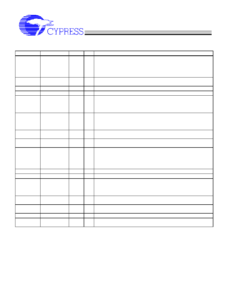
Pin Description
PIN No.
Pin Name
PWR
I/O
Description
2
S3/ REF0
VDD
I/O
3.3V 14.318 MHz clock output. This Is a power on bi-directional pin.
During power up, this pin is an input "S3" for setting the CPU
frequency (see table1, page 1) (see app note, page 5). When the
power reaches the rail, this pin becomes a buffered output of the
signal applied at Xin (typically 14.318 MHz).
48
REF1
VDD
O
This pin is a buffered output of the signal applied at Xin (typically
14.318)
4
XIN
VDD
I
14.318MHz Crystal input
5
XOUT
VDD
O
14.318MHz Crystal output
7
S1/ PCI0*
VDD
I/O
This is a power on bi-directional pin. During power up, this pin is an
input "S1" for setting the CPU frequency (see table1, page 1) (see
app not, page 5). When the power reaches the rail, this pin becomes
a PCI0 clock output.
8
S2/ PCI1*
VDD
I/O
This is a power on bi-directional pin. During power up, this pin is an
input "S2" for setting the CPU frequency (see table1, page 1) (see
app not, page 5). When the power reaches the rail, this pin becomes
a PCI1 clock output.
9,11,12,13,
14
PCI(2:6)
VDD
O
3.3V PCI clock outputs.
25
24/48MHz
VDD
O
This pin is programmable to 24MHz or 48 MHz clock output through
SMBus. It defaults to 24MHz at power up.
26
S0 / 48MHz*
VDD
I/O
This is a power on bi-directional pin. During power up, this pin is an
input "S0" for setting the CPU frequency (see table1, page 1) (see
app note, page 5). When the power reaches the rail, this pin becomes
a 48MHz clock output. This clock conforms to the USB spec. of
+167ppm.
28
SDATA
VDD
I
SMBus compatible SDATA input. Has an internal pull-up (>100K
)
29
SCLK
VDD
I
SMBus compatible SCLK input. Has an internal pull-up (>100K
)
17,18,20,21,
28,29,31,32,
34,35,37,38,
40,41
SDRAM(0:13)
VDD
O
3.3V SDRAM clock outputs. See table1, p.1 for frequency selection.
43,45,46
CPU(0:2)
VDDC
O
2.5V or 3.3V Host bus clock outputs. See table 1, page 1 for
frequency selection.
1,6,15,19,
27, 30,36,42
VDD
-
3.3V Common Power Supply
47
VDDC
-
2.5V or 3.3V Power Supply's for CPU (0:2) clock outputs.
3,10,16,22,
33,39,44
VSS
-
Common Ground pin.
A bypass capacitor (0.1
µ
F) should be placed as close as possible to each positive power pin. If these bypass capacitors
are not close to the pins their high frequency filtering characteristic will be cancelled by the lead inductance of the traces.
*Note: These pins have pulldown resistors, typical value 250
.
PC133 Clock Generator for SiS630/Pentium
Æ
III & SiS540/Socket7 Applications
Cypress Semiconductor Corporation
525 Los Coches St.
Document#: 38-07035 Rev. **
05/02/2001
Milpitas, CA 95035. Tel: 408-263-6300, Fax: 408-263-6571
Page 3 of 18
http://www.cypress.com
APPROVED PRODUCT
C9630
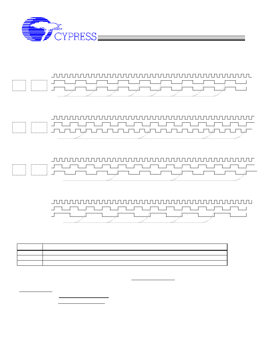
Device Clock Phase Relationships
Fig.3
Frequency Smooth Switching Groups
Group
S(4:0)
2
00000, 00011, 00110, 01010, 10000, 10101
3
00100, 00101, 01000, 01001, 01011, 01100, 01110, 01111, 10011, 10100, 10110, 11000, 11001
Table 2
Table 2 above describes 3 different groups of frequencies. Within the same group, frequency may be switched through
SMBus byte 0 without causing any glitching or clock discontinuity at the CPU(0:2) outputs, therefore allowing frequency
smooth switching of the clock.
Switching frequency from one group to another is permitted but will cause the CPU(0:2) clocks to jump immediately to
the next frequency. (non smooth switching.).
Internal VCO
Internal VCO
Internal VCO
SDRAM
to CPU
or
CPU
to SDRAM
Applicable to the follow ing selection: S(4:0) = 00100
TSkew 3
Condition 3: CPU Frequency = 1.3 X SDRAM Frequency or SDRAM Frequency = 1.3 X CPU Frequency
Applicable to the follow ing selections: S(4:0) = 00000, 00010, 00110, 01010, 10000, 10010, 10101
Condition 2: CPU Frequency = 1.5 X SDRAM Frequency or SDRAM Frequency = 1.5 X CPU Frequency
Condition 1: CPU Frequency = SDRAM Frequency
TSkew 3
Applicable to the follow ing selections: S(4:0) = 00011, 00101, 01100, 01110, 10011, 10100, 10110, 11000, 11001
TSkew 3
Applicable to the follow ing selections: S(4:0) = 00001, 00111, 01000, 01001, 01011, 01101, 01111, 10001, 10111,11010, 11011, 11100, 11101, 11110, 11111
Condition 4: SDRAM Frequency = 2 X CPU Frequency
TSkew 3
or
CPU
SDRAM
to CPU
to SDRAM
or
CPU
SDRAM
to CPU
to SDRAM
SDRAM
CPU
Internal VCO
PC133 Clock Generator for SiS630/Pentium
Æ
III & SiS540/Socket7 Applications
Cypress Semiconductor Corporation
525 Los Coches St.
Document#: 38-07035 Rev. **
05/02/2001
Milpitas, CA 95035. Tel: 408-263-6300, Fax: 408-263-6571
Page 4 of 18
http://www.cypress.com
APPROVED PRODUCT
C9630
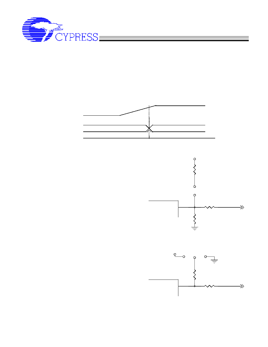
Power on Bi-Directional Pins
Power Up Condition:
Pins 2,7,8,and 26 are Power up bi-directional pins used for selecting the host frequency in page 1, table 1. During
power-up of the device, these pins are in input mode (see Fig 4, below), therefore; they are considered input select pins
internal to the IC. After a settling time, the selection data is latch into the internal control register and these pins become
a clock outputs.
-
Hi-Z Input
Toggle Outputs
ower Supply
amp
Select data is latched into register, then pin becomease ref clock output signal.
REF0 / S3
PCI0 / S1
PCI1 / S2
48MHZ / S0
VDD Rail
Strapping Resistor Options:
The power up bi-directional pins have a large value pull-
down each (250K
)
, therefore, a selection "0" is the
default. If the system uses a slow power supply (over
5mS settling time), then it is recommended to use an
external Pull-Down (Rdn) in order to insure a Low
selection. In this case, the designer may choose one of
two configurations, see Fig.5A and B.
Fig. 5A represents an additional pull down resistor Rdn
= 50K
connected from the pin to the ground plane,
which allows a faster pull to a low level.
If a selection "1" is desired, then a jumper is placed on
JP1 to a Rup = 10K
resistor as implemented as
shown in Fig.5A. Please note the selection resistors
(Rup and Rdn
)
are placed before the Damping resistor
(Rd) close to the pin.
Fig. 5B represent a single resistor 10K
connected to a
3-way jumper, JP2. When a "1" selection is desired, a
jumper is placed between leads1 and 3. When a "0"
selection is desired, a jumper is placed between leads 3
and 2.
Fig.4
Fig.5A
Fig.5B
1
2
3
Load
Load
VDD
VDD
IMIC9630
Bidirectional
10K
50K
Rd
JP1
IMIC9630
Bidirectional
Rd
10K
JP2
PC133 Clock Generator for SiS630/Pentium
Æ
III & SiS540/Socket7 Applications
Cypress Semiconductor Corporation
525 Los Coches St.
Document#: 38-07035 Rev. **
05/02/2001
Milpitas, CA 95035. Tel: 408-263-6300, Fax: 408-263-6571
Page 5 of 18
http://www.cypress.com
APPROVED PRODUCT
C9630
2-Wire SMBus Control Interface
The 2-wire control interface implements a read/write slave only interface according to SMBus specification (IC12, 1996).
The device can be read back by using standard SMBus command bytes. Sub addressing is not supported, thus all
preceding bytes must be sent in order to change one of the control bytes. The 2-wire control interface allows each clock
output to be individually enabled or disabled. 100 Kbits/second (standard mode) data transfer is supported.
During normal data transfer, the SDATA signal only changes when the SCLK signal is low, and is stable when SCLK is
high. There are two exceptions to this. A high to low transition on SDATA while SCLK is high is used to indicate the
start of a data transfer cycle. A low to high transition on SDATA while SCLK is high indicates the end of a data transfer
cycle. Data is always sent as complete 8-bit bytes, after which an acknowledge is generated. The first byte of a transfer
cycle is a 7-bit address with a Read/Write bit (R/W#) as the LSB. R/W# = 1 in read mode. R/W# = 0 in write mode.
A maximum of 10 bytes of data may be written/Read Data is transferred MSB first at a max rate of 100kbits/S.The
device will not respond to any other control interface conditions.
In the Write mode (See fig6A, p.9), the clock gen. acknowledges Address Byte, D2, then receives two additional bytes:
1) "Command Code " byte, and
2) "Byte Count" byte. Must be programmed to FF for correct operation.
Although the data (bits) in these two bytes are considered "don't care"; they must be sent and will be acknowledged.
Subsequently, the below-described sequence (Byte 0, Byte 1, Byte2,) will be valid and acknowledged.
In the Read Mode (See fig6B, p.9), the clock gen. acknowledges Address D3, and immediately transmits data starting
with Byte count, then Byte 0, 1, 2, ... After each transmitted byte, this device waits for an acknowledge before
transmitting the next byte.
Serial Control Registers
NOTE: Power up conditions for each bit are listed in the "@Pup" column.
Byte 0: Frequency, Function Select Register
Bit
@Pup
Pin#
Description, see page 8 for SSCG description.
7
0
n/a
S4 (for frequency table 3, selection by software via SMBus), selection valid if bit3 = 1
6
0
n/a
S2 (for frequency table 3, selection by software via SMBus), selection valid if bit3 = 1
5
0
n/a
S1 (for frequency table 3, selection by software via SMBus), selection valid if bit3 = 1
4
0
n/a
S0 (for frequency table 3, selection by software via SMBus), selection valid if bit3 = 1
3
0
n/a
0 = frequency selected by hardware, pins
2,7,8,26
1 = frequency selection via SMBus byte0.
bits 4,5,6,2,7
2
0
n/a
S3 (for frequency table 3, selection by software via SMBus), selection valid if bit3 = 1
1
0
n/a
0 = Spread Spectrum disabled
1 = Spread spectrum enabled
0
0
n/a
0 = Running
1 = Test mode.