
Three-PLL General-Purpose
EPROM-Programmable Clock Generator
CY2081
Cypress Semiconductor Corporation
∑
3901 North First Street
∑
San Jose
∑
CA 95134
∑
408-943-2600
Document #: 38-07136 Rev. *A
Revised December 14, 2002
1
Features
∑ Factory-EPROM configurable for quick availability and
prototyping
∑ General purpose clock synthesizer for all applications
≠ such as modems, disk drives, CD-ROM drives, Video
CD players, games, set-top boxes, data/telecommuni-
cations, etc.
∑ Three independent configurable clock outputs
∑ Outputs ranging from 500 kHz to 100 MHz (5V) and up
to 80 MHz for 3.3V operation
∑ Configurable output control pin (pin 8) can be used as
an output enable, power-down, suspend or select line.
∑ Phase-locked loop oscillator input derived from exter-
nal crystal (10 MHz to 25 MHz) or external reference
clock (1 MHz to 30 MHz)
∑ 3.3V or 5V operation (factory configured)
∑ 8-pin 150-mil packaging achieves minimum footprint
for space-critical applications
∑ Sophisticated internal loop filter requires no external
components or manufacturing tweaks as commonly re-
quired with external filters
Functional Description
The CY2081 is a general-purpose clock synthesizer designed
for use in applications such as modems, disk drives, CD-ROM
drives, Video CD players, games, set-top boxes and data/tele-
communications. This devices offers three configurable clock
outputs in an 8-pin 150-mil SOIC package and can be config-
ured to operate off either a 3.3V or 5V power supply. The
on-chip reference oscillator is designed for 10 MHz to 25 MHz
crystals. Alternatively, a reference clock between 1 MHz and
30 MHz can be used.
The CY2081 also features an output control pin (pin 8), which
can be configured as an output enable, power down, frequen-
cy select, or suspend input. This gives the user the ability to
three-state the output, power down the device, change the
CLKA output frequency during operation, or suspend any of
the outputs. Asserting the PD input will result in all the PLLs
and the outputs being shut down. The PLLs will have to re-lock
when the PD input is deasserted.
The CY2081 outputs three clocks: CLKA, CLKB, and CLKC,
whose frequencies can possess any value within the specified
range. Additionally, the reference frequency can be obtained
on any output. Custom configurations with user-defined fea-
tures and frequencies can be obtained by filling out the custom
configuration form located at the back of this data sheet and
contacting your local Cypress representative.
The CY2081 can replace multiple Metal Can Oscillators
(MCO) in a synchronous system, providing cost and board
space savings to manufacturers. Hence, this device is ideally
suited for applications that require multiple, accurate, and sta-
ble clocks synthesized from low-cost generators in small pack-
ages. A hard disk drive is an example of such an application.
In this case, CLKA drives the PLL in the Read Controller, while
CLKB and CLKC drive the MCU and associated sequencers.
Consider using the CY2291, CY2292, or CY2907 for applica-
tions that require more than three output clocks.
Pin Configuration
1
2
3
4
5
8
7
6
CLKA
GND
XTALIN
XTALOUT
V
DD
CLKC
CLKB
SOIC
Top View
Logic Block Diagram
XTALOUT
XTALIN
Reference
Oscillator
PLL 1
CLKA
CLKB
CLKC
EPROM-
Configurable
Multiplexer
and Divide
Logic
PLL 2
PLL 3
OE/PD/FS/SUSPEND
OE/PD/FS/SUSPEND
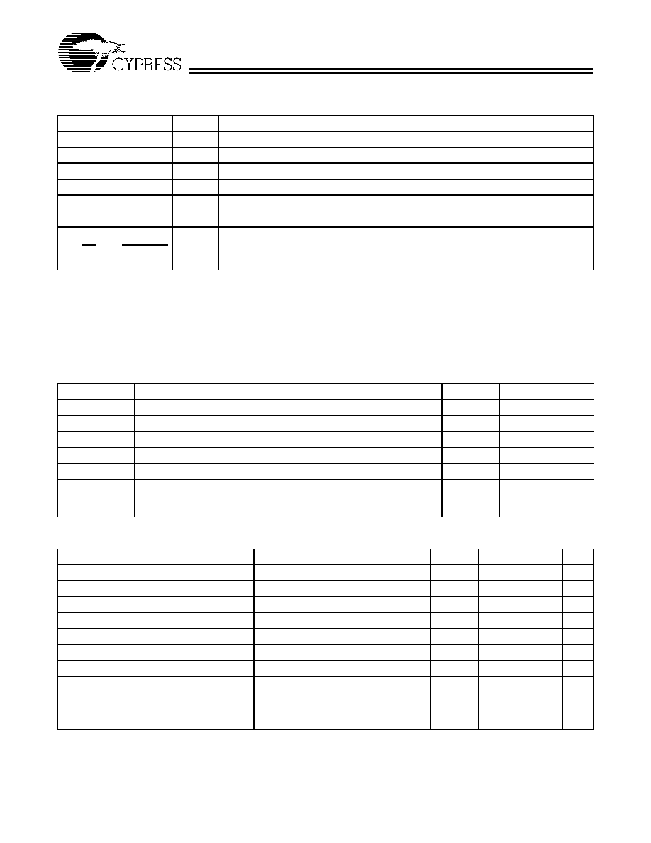
CY2081
Document #: 38-07136 Rev. *A
Page 2 of 6
Maximum Ratings
(Above which the useful life may be impaired. For user guide-
lines, not tested.)
Supply Voltage ............................................... ≠0.5V to +7.0V
DC Input Voltage......................................≠0.5V to V
DD
+0.5V
Storage Temperature ................................. ≠65
∞
C to +150
∞
C
Junction Temperature ...................................................150
∞
C
Static Discharge Voltage............................................ >2000V
(per MIL-STD-883, Method 3015)
Pin Summary
Name
Number
Description
CLKA
1
Configurable Clock Output
GND
2
Ground
XTALIN
[1]
3
Reference Crystal Input or External Reference Clock Input
XTALOUT
[1,2]
4
Reference Crystal Feedback
CLKB
5
Configurable Clock Output
CLKC
6
Configurable Clock Output
V
DD
7
Voltage Supply
OE / PD / FS / SUSPEND 8
Output control pin; either active-HIGH Output Enable, active-LOW power down, CLKA
Frequency Select, or active-LOW Suspend input
Operating Conditions
[3]
Parameter
Description
Min.
Max.
Unit
V
DD
Supply Voltage
4.5 (3.0)
5.5 (3.6)
V
T
A
Operating Temperature, Ambient
0
70
∞
C
C
L
Max. Load Capacitance per output
25 (15)
pF
f
REF
External Reference Crystal
10.0
25.0
MHz
f
REF
External Reference Clock
[4, 5]
1.0
30.0
MHz
t
PU
Power-up time for all VDD's to reach minimum specified voltage (power
ramps must be monotonic)
0.05
50
ms
Electrical Characteristics
V
DD
= 5V (3.3V)
±
10%, T
A
= 0
∞
C to +70
∞
C
Parameter
Description
Conditions
Min.
Typ.
Max.
Unit
V
OH
HIGH-Level Output Voltage
I
OH
= ≠4.0 mA
2.4
V
V
OL
LOW-Level Output Voltage
I
OL
= 4.0 mA
0.4
V
V
IH
HIGH-Level Input Voltage
[6]
Except Crystal Pins
2.0
V
V
IL
LOW-Level Output Voltage
[6]
Except Crystal Pins
0.8
V
I
IH
Input HIGH Current
V
IN
= V
DD
≠ 0.5V
<100
150
µ
A
I
IL
Input LOW Current
V
IN
= 0.5V
<100
150
µ
A
I
OZ
Output Leakage Current
Three State Outputs
250
µ
A
I
DD
V
DD
Supply Current
[7]
V
DD
= V
DD
max. 5V (3.3V) operation, C
L
= 25 pF (15 pF)
40 (24)
60 (40)
mA
I
DDS
V
DD
Power Supply Current in
Power-down Mode
Power-down Active, 5V Operation
100
200
µ
A
CY2081
Document #: 38-07136 Rev. *A
Page 3 of 6
Notes:
1.
For best accuracy, use a parallel-resonant crystal, C
L
=17 pF.
2.
Float XTALOUT pin if XTALIN is driven by reference clock (as opposed to an external crystal).
3.
Electrical parameters are guaranteed with these operating conditions. Values for 3.3V operation are shown in parentheses.
4.
External input reference clock must have a duty cycle between 40% and 60%, measured at V
DD
/2.
5.
Please refer to application note "Crystal Oscillator Topics" for information on AC-coupling the external input reference clock.
6.
Xtal inputs have CMOS thresholds.
7.
Load = max, typical configuration, f
REF
= 14.318 MHz. Specific configurations may vary.
Electrical Characteristics
V
DD
= 5V (3.3V)
±
10%, T
A
= 0
∞
C to +70
∞
C
Parameter
Description
Conditions
Min.
Typ.
Max.
Unit
Switching Characteristics
[8]
Parameter
Name
Description
Min.
Typ.
Max.
Unit
t
1
Output Period
Clock output range, 5V operation
10
[100 MHz]
2000
[500 KHz]
ns
t
1
Output Period
Clock output range, 3.3V operation
12.5
[80 MHz]
2000
[500 KHz]
ns
t
1A
Clock Jitter
[9]
Peak-to-peak period jitter,% of clock period
(f
OUT
4 MHz)
<0.5
1
%
t
1B
Clock Jitter
[9]
Peak-to-peak period jitter
(4 MHz
f
OUT
16 MHz)
<0.7
1
ns
t
1C
Clock Jitter
[9]
Peak-to-peak period jitter
(16 MHz
<
f
OUT
50 MHz)
<400
500
ps
t
1D
Clock Jitter
[9]
Peak-to-peak period jitter
(f
OUT
>
50 MHz)
<250
350
ps
Output Duty Cycle
[10]
Duty cycle for outputs, defined as t
2
˜
t
1
[11]
f
OUT
> 66.67 MHz
40%
50%
60%
Duty cycle for outputs, defined as t
2
˜
t
1
[11]
f
OUT
66.67 MHz
45%
50%
55%
t
3
Rise time
Output clock rise time
[12]
at C
L
=25 pF (15 pF
at 3.3V operation)
3
5
ns
t
4
Fall time
Output clock fall time
[12]
at C
L
=25 pF (15 pF
at 3.3V operation)
2.5
4
ns
t
5
Frequency Slew Rate Rate of change of frequency of CLKA
1
5
40
MHz/
ms
t
6
Power Up Stabiliza-
tion Time
Output clock stable time after power up
< 25
50
ms
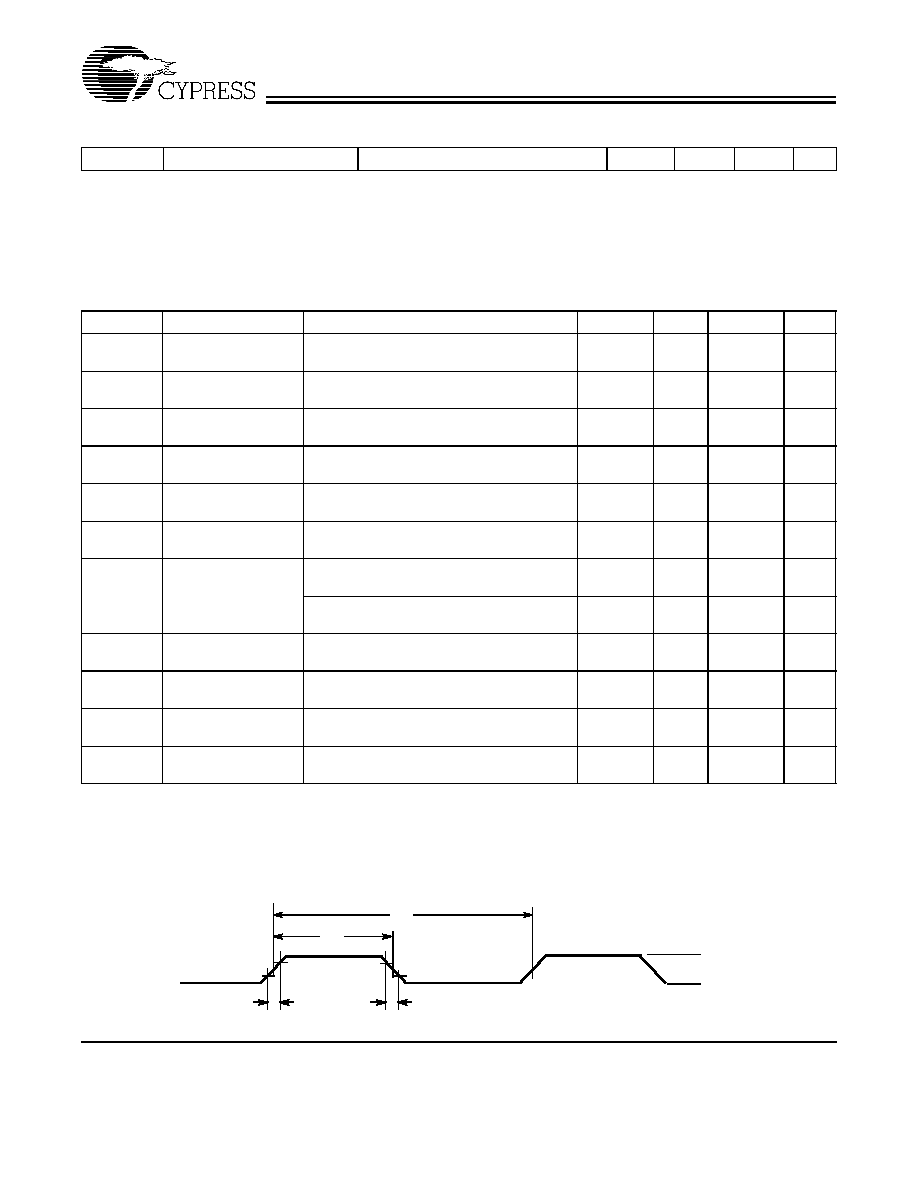
Switching Waveforms
All Outputs Duty Cycle and Rise/Fall Time
OUTPUT
t
3
t
4
t
2
t
1
2.4V
0.4V
0.4V
2.4V
3.3V
0V
CY2081
Document #: 38-07136 Rev. *A
Page 4 of 6
Customer Configuration Request Procedure
The CY2081 is programmed at the wafer level, and is there-
fore only available as a factory programmed device. There is
no field programming for the CY2081.
For CY2081 programmed configurations, design opportunities
must be 50 Ku per year in production. If the design opportunity
does not meet the factory minimums, the design can be imple-
mented using the CY2292 (3-PLLs, 16-SOIC, field program-
mable), or the CY22381 (3-PLLs, 8-SOIC, field programma-
ble).
For factory programmed samples, all requests must be sub-
mitted to your local Cypress FAE or sales representative. The
method to use to request factory configurations is:
Use CyClocks software. This software automatically calcu-
lates the output frequencies that can be generated by the
CY2081 and provides a printout of final pinout. Output fre-
quencies requested will be matched as closely as the internal
PLL divider and multiplier options allow. This printout and the
design entry file produced by CyClocks (<filename>.ENT) can
be submitted (in electronic format) to your local FAE or sales
representative. CyClocks software is available free of charge
from the Cypress website (http://www.cypress.com) or from
your local FAE or sales representative.
Once the custom request has been processed you will receive
a part number with a three-digit extension (e.g.,
CY2081SC-357) specific to the frequencies and pinout of your
device. This will be the part number used for samples requests
and production orders.
CyClocks is a trademark of Cypress Semiconductor Corporation.
Notes:
8.
Guaranteed by design, not 100% tested.
9.
Jitter varies with configuration. All standard configurations sample tested at the factory conform to this limit. For more information on jitter, please refer to
the application note: "Jitter in PLL-Based Systems."
10. Reference Output duty cycle depends on XTALIN duty cycle.
11. Measured at 1.4V.
12. Measured between 0.4V and 2.4V.
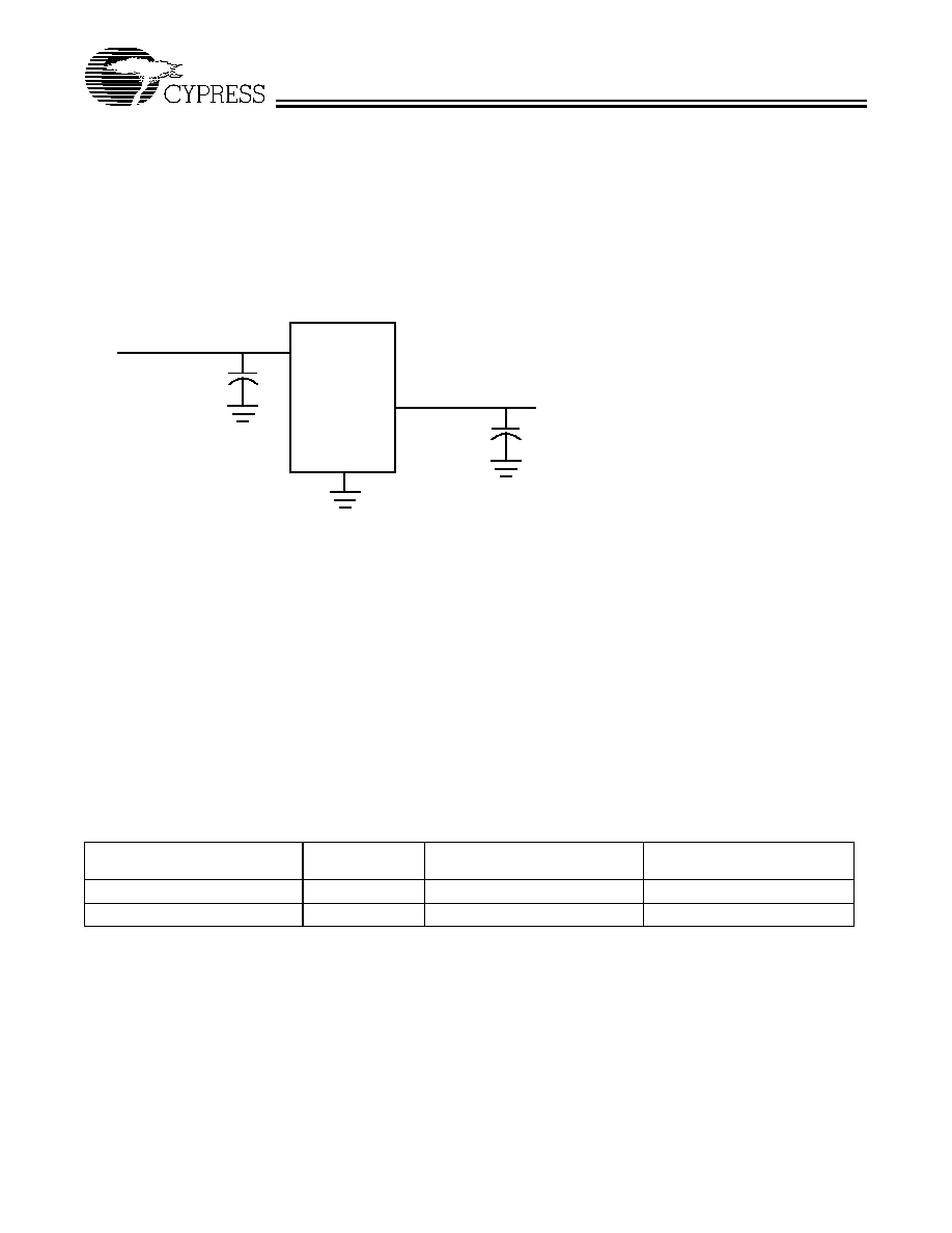
Switching Waveforms
Test Circuit
0.1
µ
F
V
DD
CLK output
C
LOAD
GND
7
2
OUTPUTS
Ordering Information
Ordering Code
Package Name
Package Type
Operating Range
CY2081SC-XXX
S8
8-Pin (150-Mil) SOIC
5.0V, Commercial
[13]
CY2081SL-XXX
S8
8-Pin (150-Mil) SOIC
3.3V, Commercial
[13]
Note:
13. 0∞C to +70∞C
CY2081
Document #: 38-07136 Rev. *A
Page 5 of 6
© Cypress Semiconductor Corporation, 2001. The information contained herein is subject to change without notice. Cypress Semiconductor Corporation assumes no responsibility for the use
of any circuitry other than circuitry embodied in a Cypress Semiconductor product. Nor does it convey or imply any license under patent or other rights. Cypress Semiconductor does not authorize
its products for use as critical components in life-support systems where a malfunction or failure may reasonably be expected to result in significant injury to the user. The inclusion of Cypress
Semiconductor products in life-support systems application implies that the manufacturer assumes all risk of such use and in doing so indemnifies Cypress Semiconductor against all charges.
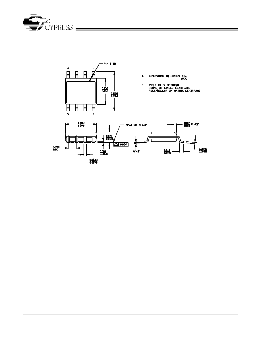
Package Diagram
8-Lead (150-Mil) SOIC S8
51-85066-A