
1Kx4 Static RAM
CY7C148
CY7C149
Cypress Semiconductor Corporation
∑
3901 North First Street
∑
San Jose
∑
CA 95134
∑
408-943-2600
Document #: 38-05059 Rev. **
Revised September 18, 2001
49
Features
∑ Automatic power-down when deselected (7C148)
∑ CMOS for optimum speed/power
∑ 25-ns access time
∑ Low active power
-- 440 mW (commercial)
-- 605 mW (military)
∑ Low standby power (7C148)
-- 82.5 mW (25-ns version)
-- 55 mW (all others)
∑ 5-volt power supply
±
10% tolerance, both commercial
and military
∑ TTL-compatible inputs and outputs
Functional Description
The CY7C148 and CY7C149 are high-performance CMOS
static RAMs organized as 1024 by 4 bits. Easy memory expan-
sion is provided by an active LOW chip select (CS) input and
three-state outputs. The CY7C148 remains in a low-power
mode as long as the device remains unselected; i.e., (CS) is
HIGH, thus reducing the average power requirements of the
device. The chip select (CS) of the CY7C149 does not affect
the power dissipation of the device.
Writing to the device is accomplished when the chip select
(CS) and write enable (WE) inputs are both LOW. Data on the
I/O pins (I/O
0
through I/O
3
) is written into the memory loca-
tions specified on the address pins (A
0
through A
9
).
Reading the device is accomplished by taking chip select (CS)
LOW while write enable (WE) remains HIGH. Under these
conditions, the contents of the location specified on the
address pins will appear on the four data I/O pins.
The I/O pins remain in a high-impedance state when chip se-
lect (CS) is HIGH or write enable (WE) is LOW.
Logic Block Diagram
Pin Configurations
64 x 64
ARRAY
1
2
3
4
5
6
7
8
9
10
11
12
13
14
18
17
16
15
Top View
DIP
A
8
A
7
A
6
A
3
A
2
A
5
A
9
COLUMN
DECODER
ROW DECODER
SE
NSE
A
M
P
INPUTBUFFER
POWER
DOWN
(7C148)
WE
CS
I/O
0
A5
A4
A3
A 0
A1
A2
WE
GND
CS
VCC
A7
A8
A9
I/O
1
A
1
A
0
A
4
A6
I/O 0
I/O 1
I/O 2
I/O 3
I/O
2
I/O
3
6
3
4
7
8 9
2 1
5
1011
12
13
1817
16
15
14
A4
A13
A10
A11
A12
A8
A9
I/O 0
I/O 1
I/O2
A
5
A
6
V CC A
7
GND
I/0
3
WE
Top View
LCC
CS
C148≠1
C148≠2
C148≠3
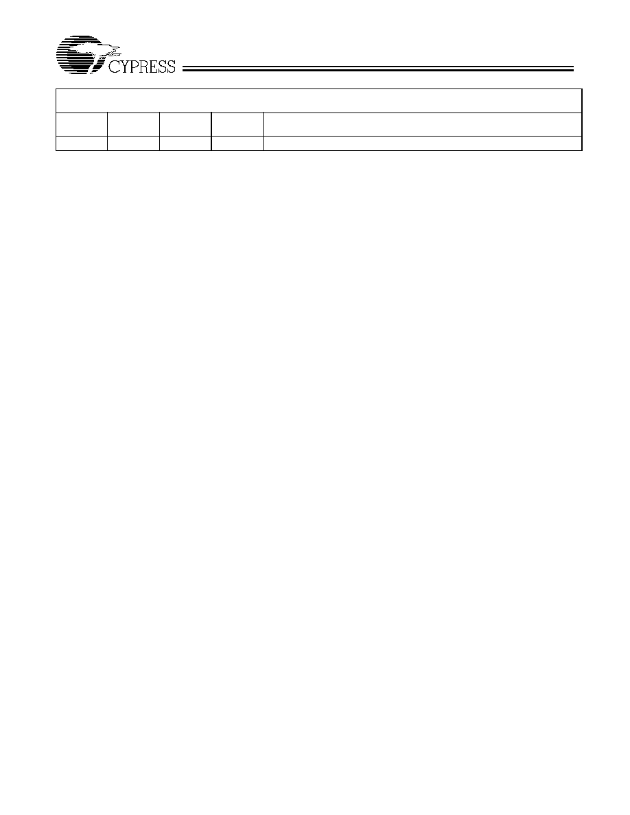
Selection Guide
7C148
-
25
7C148
-
35
7C148
-
45
7C149
-
25
7C149
-
35
7C149
-
45
Maximum Access Time (ns)
25
35
45
25
35
45
Maximum Operating
Current (mA)
Commercial
90
80
80
90
80
80
Military
110
110
110
110
Maximum Standby
Current (mA)
Commercial
15
10
10
Military
10
10

CY7C148
CY7C149
Document #: 38-05059 Rev. **
Page 2 of 9
Maximum Ratings
(Above which the useful life may be impaired. For user guide-
lines, not tested.)
Storage Temperature
......................................-
65
∞
C to+150
∞
C
Ambient Temperature with
Power Applied
...................................................-
55
∞
C to+125
∞
C
Supply Voltage to Ground Potential
(Pin 18 to Pin 9)
....................................................-
0.5V to+7.0V
DC Voltage Applied to Outputs
in High Z State
......................................................-
0.5V to+7.0V
DC Input Voltage
.................................................-
3.0V to +7.0V
Output Current into Outputs (LOW)............................. 20 mA
Static Discharge Voltage ........................................... >2001V
(per MIL-STD-883, Method 3015)
Latch-Up Current ..................................................... >200 mA
Operating Range
Range
Ambient
Temperature
V
CC
Commercial
0
∞
C to +70
∞
C
5V
±
10%
Military
[1]
-
55
∞
C to +125
∞
C
5V
±
10%
Note:
1.
T
A
is the "instant on" case temperature.
Electrical Characteristics
Over the Operating Range
[2]
Parameter
Description
Test Conditions
7C148
-
25
7C149
-
25
7C148
-
35, 45
7C149
-
35, 45
Unit
Min.
Max.
Min.
Max.
V
OH
Output HIGH Voltage
V
CC
= Min., I
OH
=
-
4.0 mA
2.4
2.4
V
V
OL
Output LOW Voltage
V
CC
= Min., I
OL
= 8.0 mA
0.4
0.4
V
V
IH
Input HIGH Voltage
2.0
6.0
2.0
6.0
V
V
IL
Input LOW Voltage
-
3.0
0.8
-
3.0
0.8
V
I
IX
Input Load Current
GND < V
I
< V
CC
-
10
10
-
10
10
µ
A
I
OZ
Output Leakage Current
GND < V
O
< V
CC
Output Disabled
-
50
50
-
50
50
µ
A
I
CC
V
CC
Operating
Supply Current
Max. V
CC
, CS < V
IL
,
Output Open
Com'l
90
80
mA
Mil
110
I
SB
Automatic CS
Power-Down Current
Max. V
CC
, CS > V
IH
7C148
Only
Com'l
15
10
mA
Mil
10
I
PO
Peak Power-On
Current
[3]
Max. V
CC
, CS > V
IH
7C148
Only
Com'l
15
10
mA
Mil
10
I
OS
Output Short
Circuit Current
[4]
GND < V
O
< V
CC
Com'l
±
275
±
275
mA
Mil
±
350
Capacitance
[5]
Parameter
Description
Test Conditions
Max.
Unit
C
IN
Input Capacitance
T
A
= 25
∞
C, f = 1 MHz,
V
CC
= 5.0V
8
pF
C
OUT
Output Capacitance
8
pF
Notes:
2.
See the last page of this specification for Group A subgroup testing information.
3.
A pull-up resistor to V
CC
on the CS input is required to keep the device deselected during V
CC
power-up. Otherwise current will exceed values given (CY7C148
only).
4.
For test purposes, not more than 1 output should be shorted at one time. Duration of the short circuit should not exceed 30 seconds.
5.
Tested initially and after any design or process changes that may affect these parameters.
CY7C148
CY7C149
Document #: 38-05059 Rev. **
Page 3 of 9
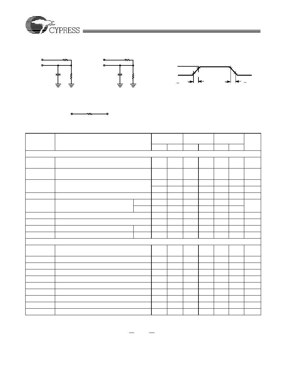
AC Test Loads and Waveforms
3.0V
5V
OUTPUT
R1481
R2
255
30 pF
INCLUDING
JIG AND
SCOPE
GND
90%
10%
90%
10%
< 10 ns
< 10 ns
5V
OUTPUT
R1481
R2
255
5 pF
INCLUDING
JIG AND
SCOPE
(a)
(b)
OUTPUT
1.73V
Equivalent to:
TH… VENIN EQUIVALENT
ALL INPUT PULSES
C148≠4
C148≠5
167
Switching Characteristics
Over the Operating Range
[2]
Parameter
Description
7C148
-
25
7C149
-
25
7C148
-
35
7C149
-
35
7C148
-
45
7C149
-
45
Unit
Min.
Max.
Min.
Max.
Min.
Max.
READ CYCLE
t
RC
Address Valid to Address Do Not Care Time
(Read Cycle Time)
25
35
45
ns
t
AA
Address Valid to Data Out Valid Delay
(Address Access Time)
25
35
45
ns
t
ACS1
t
ACS2
Chip Select LOW to Data Out Valid (7C148 only)
25
[6]
35
45
ns
30
[7]
35
45
ns
t
ACS
Chip Select LOW to Data Out Valid (7C149 only)
15
15
20
ns
t
LZ
[8]
Chip Select LOW to Data Out On
7C148
8
10
10
ns
7C149
5
5
5
t
HZ
[8]
Chip Select HIGH to Data Out Off
0
15
0
20
0
20
ns
t
OH
Address Unknown to Data Out Unknown Time
0
0
5
ns
t
PD
Chip Select HIGH to Power-Down Delay
7C148
20
30
30
ns
t
PU
Chip Select LOW to Power-Up Delay
7C148
0
0
0
ns
WRITE CYCLE
t
WC
Address Valid to Address Do Not Care
(Write Cycle Time)
25
35
45
ns
t
WP
[9]
Write Enable LOW to Write Enable HIGH
20
30
35
ns
t
WR
Address Hold from Write End
5
5
5
ns
t
WZ
[8]
Write Enable to Output in High Z
0
8
0
8
0
8
ns
t
DW
Data in Valid to Write Enable HIGH
12
20
20
ns
t
DH
Data Hold Time
0
0
0
ns
t
AS
Address Valid to Write Enable LOW
0
0
0
ns
t
CW
[9]
Chip Select LOW to Write Enable HIGH
20
30
40
ns
t
OW
[8]
Write Enable HIGH to Output in Low Z
0
0
0
ns
t
AW
Address Valid to End of Write
20
30
35
ns
Notes:
6.
Chip deselected greater than 25 ns prior to selection.
7.
Chip deselected less than 25 ns prior to selection.
8.
At any given temperature and voltage condition, t
HZ
is less than t
LZ
for all devices. Transition is measured
±
500 mV from steady-state voltage with specified
loading in part (b) of AC Test Loads.
9.
The internal write time of the memory is defined by the overlap of CS LOW and WE LOW. Both signals must be LOW to initiate a write and either signal can
terminate a write by going high. The data input set-up and hold timing should be referenced to the rising edge of the signal that terminates the write.
CY7C148
CY7C149
Document #: 38-05059 Rev. **
Page 4 of 9
Switching Waveforms
Notes:
10. WE is HIGH for read cycle.
11. Device is continuously selected, CS = V
IL
.
12. Address valid prior to or coincident with CS transition LOW.
Read Cycle No. 1
Read Cycle No. 2
Write Cycle No. 1 (WE Controlled)
ADDRESS
50%
DATA OUT
PREVIOUS DATA VALID
DATA VALID
t
RC
t
AA
50%
DATA VALID
t
RC
t
ACS
t
LZ
t
PU
DATA OUT
HIGH IMPEDANCE
IMPEDANCE
ICC
ISB
t
HZ
t
PD
CS
HIGH
t
WC
DATA≠IN VALID
DATA UNDEFINED
HIGH IMPEDANCE
t
CW
t
AW
t
AS
t
WP
t
WA
t
DH
V
CC
SUPPLY
CURRENT
t
WZ
t
OW
t
DW
CS
WE
DATA IN
DATA OUT
ADDRESS
t
OH
C148≠6
C148≠7
C148≠8
[10,11]
[10,12]
CY7C148
CY7C149
Document #: 38-05059 Rev. **
Page 5 of 9
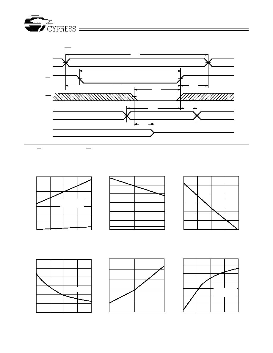
Notes:
13. If CS goes HIGH simultaneously with WE HIGH, the output remains in a high-impedance state.
Switching Waveforms
(continued)
Write Cycle No. 2 (CSControlled)
t
WC
DATA UNDEFINED
HIGH IMPEDANCE
t
CW
t
AW
t
WP
t
WR
t
DH
t
WZ
t
DW
ADDRESS
CS
WE
DATA IN
DATA OUT
C148≠9
DATA
IN
VALID
[13]
Typical DC and AC Characteristics
1.2
1.4
1.0
0.6
0.4
0.2
4.0
4.5
5.0
5.5
6.0
1.6
1.4
1.2
1.0
0.8
-
55
25
125
-
55
25
125
1.2
1.0
0.8
NORMA
L
I
Z
E
D
t
AA
120
100
80
60
40
20
0.0
1.0
2.0
3.0
4.0
OUT
P
UT S
O
URCE
CURRE
NT (m
A
)
SUPPLY VOLTAGE(V)
NORMALIZED SUPPLY CURRENT
vs.SUPPLY VOLTAGE
NORMALIZED ACCESS TIME
vs.AMBIENT TEMPERATURE
AMBIENT TEMPERATURE(∞C)
NORMALIZED SUPPLY CURRENT
vs.AMBIENT TEMPERATURE
AMBIENT TEMPERATURE(∞C)
OUTPUT VOLTAGE(V)
OUTPUT SOURCE CURRENT
vs.OUTPUT VOLTAGE
0.0
0.8
1.4
1.1
1.0
0.9
4.0
4.5
5.0
5.5
6.0
NORMA
L
I
Z
E
D
t
SUPPLY VOLTAGE(V)
NORMALIZED ACCESS TIME
vs.SUPPLY VOLTAGE
120
140
100
60
40
20
0.0
1.0
2.0
3.0
4.0
O
U
T
P
UT
S
I
NK
CURR
E
N
T (m
A
)
0
80
OUTPUT VOLTAGE(V)
OUTPUT SINK CURRENT
vs.OUTPUT VOLTAGE
0.6
0.4
0.2
0.0
NORMA
L
I
Z
E
D
I,
I
CC
SB
N
O
R
M
AL
IZ
ED
I,
I
CC
SB
I
SB
V
CC
=5.0V
V
IN
=5.0V
I
CC
I
CC
V
CC
=5.0V
V
CC
=5.0V
T
A
=25∞C
V
CC
=5.0V
T
A
=25∞C
I
SB
T
A
=25∞C
0.6
0.8
0
AA
1.3
1.2
V
IN
=5.0V
T
A
=25∞C

CY7C148
CY7C149
Document #: 38-05059 Rev. **
Page 6 of 9
Typical DC and AC Characteristics
3.0
2.5
2.0
1.5
1.0
0.5
0.0
1.0
2.0
3.0
4.0
NO
RM
A
L
I
Z
E
D
I
PO
SUPPLY VOLTAGE(V)
TYPICAL POWER≠ON CURRENT
vs.SUPPLY VOLTAGE(7C148)
30.0
25.0
20.0
15.0
10.0
5.0
0
200
400
600
800
DEL
T
A t
(
n
s
)
AA
CAPACITANCE (pF)
TYPICAL ACCESS TIME CHANGE
vs.OUTPUT LOADING
1.4
1.2
1.0
10
20
30
40
NORM
A
L
IZE
D
I
CC
CYCLE FREQUENCY (MHz)
NORMALIZED I
CC
vs.ACCESS TIME
0.0
5.0
0.0
1000
0.8
V
CC
=4.5V
T
A
=25∞C
0.9
1.1
1.3
T
A
=25∞C
1K
CSPULL≠UP
RESISTORTOV
CC
ISB
50
60
Ordering Information
Speed
(ns)
Ordering Code
Package
Name
Package Type
Operating
Range
25
CY7C148
-
25PC
P3
18-Lead (300-Mil) Molded DIP
Commercial
35
CY7C148
-
35PC
P3
18-Lead (300-Mil) Molded DIP
Commercial
CY7C148
-
35DMB
D4
18-Lead (300-Mil) CerDIP
Military
45
CY7C148
-
45PC
P3
18-Lead (300-Mil) Molded DIP
Commercial
CY7C148
-
45DMB
D4
18-Lead (300-Mil) CerDIP
Military
Speed
(ns)
Ordering Code
Package
Name
Package Type
Operating
Range
25
CY7C149
-
25PC
P3
18-Lead (300-Mil) Molded DIP
Commercial
35
CY7C149
-
35PC
P3
18-Lead (300-Mil) Molded DIP
Commercial
CY7C149
-
35DMB
D4
18-Lead (300-Mil) CerDIP
Military
CY7C149
-
35LMB
L50
18-Pin Rectangular Leadless Chip Carrier
45
CY7C149
-
45PC
P3
18-Lead (300-Mil) Molded DIP
Commercial
CY7C149
-
45DMB
D4
18-Lead (300-Mil) CerDIP
Military
CY7C149
-
45LMB
L50
18-Pin Rectangular Leadless Chip Carrier

CY7C148
CY7C149
Document #: 38-05059 Rev. **
Page 7 of 9
MILITARY SPECIFICATIONS
Group A Subgroup Testing
DC Characteristics
Parameters
Subgroups
I
OH
1, 2, 3
I
OL
1, 2, 3
V
IH
1, 2, 3
V
IL
Max.
1, 2, 3
I
IX
1, 2, 3
I
OZ
1, 2, 3
I
CC
1, 2, 3
I
SB
[14]
1, 2, 3
Switching Characteristics
Parameters
Subgroups
READ CYCLE
t
RC
7, 8, 9, 10, 11
t
AA
7, 8, 9, 10, 11
t
ACS1
[14]
7, 8, 9, 10, 11
t
ACS2
[14]
7, 8, 9, 10, 11
t
ACS
[15]
7, 8, 9, 10, 11
t
OH
7, 8, 9, 10, 11
WRITE CYCLE
t
WC
7, 8, 9, 10, 11
t
WP
7, 8, 9, 10, 11
t
WR
7, 8, 9, 10, 11
t
DW
7, 8, 9, 10, 11
t
DH
7, 8, 9, 10, 11
t
AS
7, 8, 9, 10, 11
t
AW
7, 8, 9, 10, 11
Notes:
14. 7C148 only.
15. 7C149 only.
CY7C148
CY7C149
Document #: 38-05059 Rev. **
Page 8 of 9
© Cypress Semiconductor Corporation, 2001. The information contained herein is subject to change without notice. Cypress Semiconductor Corporation assumes no responsibility for the use
of any circuitry other than circuitry embodied in a Cypress Semiconductor product. Nor does it convey or imply any license under patent or other rights. Cypress Semiconductor does not authorize
its products for use as critical components in life-support systems where a malfunction or failure may reasonably be expected to result in significant injury to the user. The inclusion of Cypress
Semiconductor products in life-support systems application implies that the manufacturer assumes all risk of such use and in doing so indemnifies Cypress Semiconductor against all charges.
18≠Lead(300≠Mil) CerDIP D4
MIL
-
STD
-
1835 D
-
8Config.A
18≠P in Rectangular Leadless Chip Carrier L50
MIL
-
STD
-
1835 C
-
10A
18≠Lead(300≠Mil) Molded DIP P3
CY7C148
CY7C149
Document #: 38-05059 Rev. **
Page 9 of 9
Document Title: CY7C148 / CY7C149 1K x 4 Static RAM
Document Number: 38-05059
REV.
ECN NO.
Issue
Date
Orig. of
Change
Description of Change
**
110170
09/29/01
SZV
Change from Spec number: 38-00031 to 38-05059