Direct RambusTM Clock Generator (Lite)
CY2212
Cypress Semiconductor Corporation
∑
3901 North First Street
∑
San Jose
,
CA 95134
∑
408-943-2600
Document #: 38-07466 Rev. **
Revised December 9, 2002
Features
Benefits
∑ Direct RambusTM Clock Support
One pair of differential output drivers
∑ High-speed Clock Support
400-MHz maximum, 300-MHz minimum output frequency
∑ Input Select Option
PLL multiplier select
∑ Crystal Oscillator Divider Output
LCLK = XTAL/2, not driven by phase-locked loop (PLL)
∑ Output edge-rate control
Minimize EMI
∑ 16-pin TSSOP
Space-saving, low-cost package
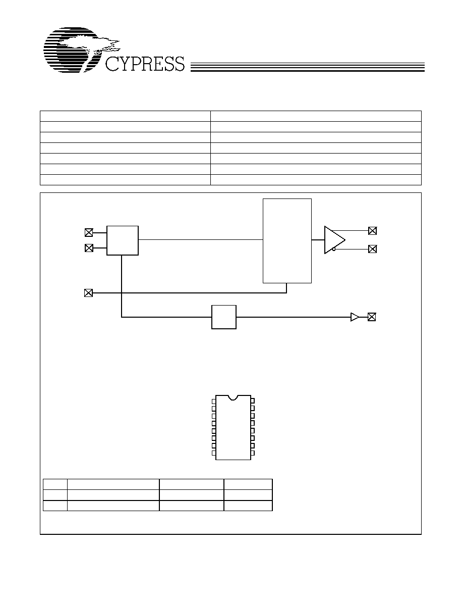
Logic Block Diagram
16-pin TSSOP
1
2
3
4
5
6
7
8
9
12
11
10
13
16
15
14
C
Y
22
12
CLKB
CLK
S
XIN
XOUT
PLL
Xtal
Oscillator
LCLK
xM
/2
TOP VIEW
CLK
VDD
S
NC
VSS
CLKB
VSS
VDD
XIN
VSSL
VDDP
NC
LCLK
VDDL
XOUT
VSSP
Xtal Value = 18.75 MHz
Pin Configuration
Frequency Select Table
S
M (PLL Multiplier)
CLK,CLKB
LCLK
0
16
300 MHz
9.375 MHz
1
64/3
400 MHz
9.375 MHz
CY2212
Document #: 38-07466 Rev. **
Page 2 of 10
Absolute Maximum Conditions
Crystal Requirements
These are the requirements for the recommended crystal to be
used with the CY2212 DRCG Lite clock source. The crystal
type is parallel resonant. The mode is fundamental. Internal
capacitors will not be implemented in the crystal oscillator
circuit. External capacitors will be needed.
Notes:
1.
At 25∞C ± 3∞C.
2.
CL = 10 pF.
3.
≠10∞C to 75∞C.
4.
At X
F
± 500 kHz.
Pin Description
Name
Pin
Description
VDDP
1
3.3V Power Supply for PLL
VSSP
2
Ground for PLL
XOUT
3
Reference Crystal Feedback
XIN
4
Reference Crystal Input
VDDL
5
1.8V Power Supply for LCLK
LCLK
6
LVCMOS Output, x1/2 Crystal Frequency
VSSL
7
Ground for LCLK
NC
8
No Connect (Reserved for Test Mode)
NC
9
No Connect (Reserved for Test Mode)
VDD
10
3.3V Power Supply
VSS
11
Ground
CLKB
12
Output Clock (complement), Connect to Rambus Channel
CLK
13
Output Clock, Connect to Rambus Channel
VSS
14
Ground
VDD
15
3.3V Power Supply
S
16
PLL Multiplier Select Input, Pull-up Resistor Internal
Parameter
Description
Min.
Max.
Unit
V
DD,ABS
Max. voltage on V
DD
, V
DDP
, or V
DDL
with respect to ground
≠0.5
4.0
V
V
I, ABS
Max. voltage on any pin with respect to ground
≠0.5
V
DD
+ 0.5
V
V
IL, ABS
Max. voltage on LCLK with respect to ground
≠0.5
V
DDL
+ 0.5
V
Parameter
Description
Min.
Max.
Unit
X
F
Frequency
14.0625
18.75
MHz
X
FTOL
Frequency Tolerance
[1]
≠15
15
ppm
X
EQRES
Equivalent Resistance
[2]
100
X
TEMP
Temperature Drift
[3]
10
ppm
X
DRIVE
Drive Level
0.01
1500
µ
W
X
MI
Motional Inductance
20.7
25.3
mH
X
IR
Insulation Resistance
500
M
X
SAR
Spurious Attenuation Ratio
[4]
3
dB
X
OS
Overtone Spurious
8
dB

CY2212
Document #: 38-07466 Rev. **
Page 3 of 10
State Transition Characteristics
Specifies the maximum settling time of the CLK, CLKB, and
LCLK outputs from device power-up. For V
DD
, V
DDP
, and V
DDL
any sequences are allowed to power-up and power-down the
CY2212 DRCG-Lite.
DC Electrical Specifications
Parameter
Description
Min.
Max.
Unit
V
DD
Supply voltage
3.04
3.56
V
V
DDL
LCLK supply voltage
1.7
2.1
V
T
A
Ambient operating temperature
0
70
∞C
V
IL
Input signal low voltage at pin S
0.35
V
DD
V
IH
Input signal high voltage at pin S
0.65
V
DD
R
PUP
Internal pull-up resistance
10
100
k
AC Electrical Specifications
Parameter
Description
Min.
Max.
Unit
f
XTAL,IN
Input frequency at crystal input
[5]
14.0625
18.75
MHz
C
IN,CMOS
Input capacitance at S pin
[6]
10
pF
DC Device Specifications
Parameter
Description
Min.
Max.
Unit
V
CM
Differential output common-mode voltage
1.35
1.75
V
V
X
Differential output crossing-point voltage
1.25
1.85
V
V
COS
Output voltage swing (p-p single-ended)
[7]
0.4
0.7
V
V
COH
Output high voltage
2.1
V
V
COL
Output low voltage
1.0
V
r
OUT
Output dynamic resistance (at pins)
[8]
12
50
V
LOH
LCLK Output high voltage at I
OH
= ≠10 mA
V
DDL
≠ 0.45V
V
DDL
V
V
LOL
LCLK Output low voltage at I
OL
= 10 mA
0
0.45
V
From
To
Transition Latency
Description
V
DD
/V
DDL
/V
DDP
On CLK/CLKB/LCLK Normal
3 ms
Time from V
DD
/V
DDL
/V
DDP
is applied and settled to
CLK/CLKB/LCLK outputs settled
AC Device Specifications
Parameter
Description
Min.
Max.
Unit
t
CYCLE
Clock cycle time
2.5
3.33
ns
t
J
Jitter over 1≠6 clock cycles at 400 MHz
[9]
100
ps
Jitter over 1≠6 clock cycles at 300 MHz
[9]
140
ps
t
JL
Long-term jitter at 400 MHz
300
ps
Long-term jitter at 300 MHz
400
ps
DC
Long-term average output duty cycle
45%
55%
t
CYCLE
t
DC,ERR
Cycle-cycle duty cycle error at 400 MHz
50
ps
Cycle-cycle duty cycle error at 300 MHz
70
ps
Notes:
5.
Nominal condition with 18.75-MHz crystal.
6.
Capacitance measured at Freq = 1 MHz, DC Bias = 0.9 V, and VAC < 100 mV.
7.
V
COS
= V
OH
≠ V
OL
.
8.
r
OUT
=
V
O
/
I
O
. This is defined at the output pins, not at the measurement point of Figure 3.
9.
Output short-term jitter specification is peak-peak and defined in Figure 10.
CY2212
Document #: 38-07466 Rev. **
Page 4 of 10
Functional Specifications
This section gives the detailed functional specifications of the
device physical layer. These specifications refer to the logical
and physical interfaces.
Crystal Input
The CY2212 receives its reference from an external crystal.
Pin XIN is the reference crystal input, and pin XOUT is the
reference crystal feedback. The parameters for the crystal are
given on page 3 of this data sheet.
Select Input
There is only one select input, pin S. This pin selects the
frequency multiplier in the PLL, and is a standard LVCMOS
input. The S pin has an internal pull-up resistor. The multiplier
selection is given on page 1 of this data sheet.
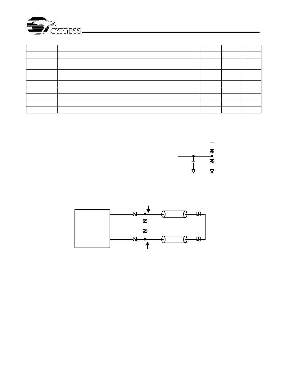
LCLK Output Driver
In addition to the Rambus clock driver outputs, there is another
clock output driver. The LCLK driver is a standard LVCMOS
output driver. Figure 1 below shows the LCLK output driver
load circuit.
RSL Clock Output Driver
Figure 2 shows the clock driver equivalent circuit.
The differential driver has a low output impedance in the range
of about 20 ohms. The driver also produces a specified voltage
swing on the channel. The nominal value of the channel
impedance, Z
CH
, is 28 ohms. Series resistor RS and parallel
resistor RP are used to set the voltage swing on the channel.
The driver output characteristics are defined together with the
external components, and the output clock is specified at the
measurement point indicated in Figure 2. The complete set of
external components for the output driver, including edge-rate
filter capacitors required for system operation, are shown in
Figure 3. The values for the external components are given in
Table 1.
The output clocks drive transmission lines, potentially long
lines. Since circuit board traces will act as lossy, imperfectly
terminated transmission lines with some discontinuities, there
will be reflections generated which will travel back to the
DRCG-Lite output driver. If the output impedance does not
match ZCH, secondary reflections will be generated that will
add to position-dependent timing uncertainty. Therefore, the
CY2212 not only provides proper output voltage swings, but
also provides a well-matched output impedance. The driver
impedance, R
OUT
, is in series with R
S
, and the combination is
in parallel with R
P
.
Notes:
10. LCLK cycle jitter and 10-cycle jitter are defined as the difference between the measured period and the nominal period as defined on page 8.
11. LCLK 10-cycle jitter specification is based on the measured value of LCLK cycle jitter as defined on page 8.
t
CR
, t
CF
Output rise and fall times (measured at 20%≠80% of output voltage)
250
500
ps
t
CR, CF
Difference between output rise and fall times on the same pin of a single
device (20%≠80%)
100
ps
BW
LOOP
PLL loop bandwidth
50 kHz
(≠3 dB)
8 MHz
(≠20 dB)
t
CYCLE,L
LCLK clock cycle time
106.6
142.2
ns
t
LR
, t
LF
LCLK output rise and fall time
1
ns
t
JC,L
LCLK cycle jitter
[10]
≠0.8
0.8
ns
t
J10,L
LCLK 10-cycle jitter
[10,11]
≠1.1 * t
JC,L
1.1 * t
JC,L
ns
DC
L
LCLK output duty cycle
40%
60%
t
CYCLE,L
AC Device Specifications
(continued)
Parameter
Description
Min.
Max.
Unit
120
120
10 pF
LCLK
Figure 1. LCLK Test Load Circuit
R
S
R
S
R
P
R
P
Z
CH
Z
CH
R
T
= Z
CH
R
T
= Z
CH
Measurement Point
Measurement Point
Differential
Driver
Figure 2. Equivalent Circuit

CY2212
Document #: 38-07466 Rev. **
Page 5 of 10
The clock driver is specified as a black-box at the packaged
pins. The output characteristics are measured after the series
resistance, R
S
. The outputs are terminated differentially, with
no applied termination voltage.
Figure 3 below shows the clock driver implemented as a push-
pull driver. When stimulating the output driver, the trans-
mission lines shown in Figure 3 can be replaced by a direct
connection to the termination resistors, R
T
. The values for the
external components are given in Table 1.
As mentioned previously, the clock driver's output impedance
matches the channel impedance. To accomplish this, each of
the output driver devices are sized to have an R
OUT
of about
20 ohms when fully turned on. R
OUT
is the dynamic output
resistance, and is defined in the DC Device Characteristics
Table on page 3 of this data sheet. Since R
OUT
is in series with
R
S
, and that combination is in parallel with R
P
, the effective
output impedance is given by:
R
P
(R
S
+ R
OUT
)/(R
P
+ R
S
+ R
OUT
).
This calculation results in a effective output impedance of
about 27 ohms for the values listed in Table 1. Since the total
impedance is dominated by the external resistors, a large
possible range of R
OUT
is allowed. When the output is transi-
tioning, the impedance of the CMOS devices increases
dramatically. The purpose of R
P
is to limit the maximum output
impedance during output transitions.
In order to control signal attenuation and EMI, clock signal
rise/fall times must be tightly controlled. Therefore, external
filter capacitors C
F
are used to control the output slew rate. In
addition, the capacitor C
MID
is used to provide AC ground at
the mid-point of the R
P
resistors.
Table 1 gives the nominal values of the external components
and their maximum acceptable tolerance, assuming
ZCH = 28 ohms.
Table 1. Output External Component Values
Parameter
Description
Value
Tolerance
Unit
R
S
Series Resistor
68
±5%
ohm
R
P
Parallel Resistor
39
±5%
ohm
C
F
Edge-rate Filter Capacitor
15
±10%
pF
C
MID
AC Ground Capacitor
0.01
±20%
µ
F
R
S
R
S
R
P
R
P
Z
CH
Z
CH
R
T
=Z
CH
R
T
=Z
CH
Measurement Point
Measurement Point
DRCG Lite
C
F
C
F
C
MID
C
MID
Figure 3. Output Driver
R
S
R
S
R
P
R
P
Z
CH
Z
CH
R
T
= Z
CH
R
T
= Z
CH
Measurement Point
DRCG Lite
C
F
C
F
C
MID
C
MID
Z
CH
Z
CH
R
T
= Z
CH
R
T
= Z
CH
Measurement Point
C
MID
R
X
R
X
R
X
R
X
Figure 4. Output Driving Two Channels