
133-MHz Spread Spectrum Clock Synthesizer/Driver
with Differential CPU Outputs
CY2220
Cypress Semiconductor Corporation
∑
3901 North First Street
∑
San Jose
∑
CA 95134
∑
408-943-2600
Document #: 38-07206 Rev. *A
Revised December 30, 2002
0
Features
Benefits
∑ Compliant to Intel
Æ
CK00 Clock Synthesizer/Driver
Specifications
Supports next generation Pentium
Æ
processors using differen-
tial clock drivers
∑ Multiple output clocks at different frequencies
-- Four pairs of differential CPU outputs, up to 133 MHz
-- Ten synchronous PCI clocks
-- Two Memory Reference clocks, 180 degrees out of
phase
-- Four AGP and Hub Link clocks at 66 MHz
-- Two 48-MHz clocks
-- Two reference clocks at 14.318 MHz
Motherboard clock generator
-- Support Multiple CPUs and a chipset
-- Support for PCI slots and chipset
-- Drives up to two Direct Rambus
TM
Clock Generators
(DRCG)
-- Supports USB host controller and SuperI/O chip
-- Supports ISA slots and I/O chip
∑ Spread Spectrum clocking
-- 31 kHz modulation frequency
-- Default is ≠0.6%, which is recommended by Intel
Enables reduction of EMI and overall system cost
∑ Power-down features
Enables ACPI compliant designs
∑ Three Select inputs
Supports up to eight CPU clock frequencies
∑ Low-skew and low-jitter outputs
Meets tight system timing requirements at high frequency
∑ OE and Test Mode support
Enables ATE and "bed of nails" testing
∑ 56-pin SSOP package
Widely available, standard package enables lower cost
Intel and Pentium are registered trademarks of Intel Corporation.
Direct Rambus is a trademark of Rambus, Inc.
Logic Block Diagram
EPROM
XTALOUT
XTALIN
14.318
MHz
OSC.
MemRef, MemRefB
SELA
CPU
PLL
REFCLK [0≠1]
CPUCLK [0≠3]
PCICLK [0≠9] (33.33 MHz)
SYS
PLL
USBCLK [0-1] (48 MHz)
MultSel1
MultSel0
SELB
SEL133
CPUCLKB [0≠3]
Divider
and
Stop Logic
SPREAD
3V66 [0≠3] (66.67 MHz)
SSOP
Top View
1
2
3
4
5
6
7
8
9
10
11
12
33
32
31
30
29
36
35
V
SSREF
34
13
14
15
16
17
18
19
20
21
22
23
24
45
44
43
42
41
37
38
39
40
48
47
46
REFCLK0/MultSel_0
REFCLK1/MultSel_1
V
DDREF
25
26
27
28
49
52
51
50
53
56
55
54
V
DDPCI
PCICLK_6
Sel133
3V66_1
3V66_2
V
SSCPU
CPUCLK_2B
V
SSMEM
V
SSPCI
PCICLK_5
PCICLK_8
USBCLK1/SelB
AV
SS
V
DDCPU
CPUCLK_3B
V
DDMEM
XTALIN
XTALOUT
PCICLK_0
PCICLK_1
PCICLK_2
PCICLK_3
V
SSPCI
PCICLK_4
V
DDPCI
PCICLK_7
V
SSPCI
PCICLK_9
V
DDPCI
V
SSUSB
USBCLK0/SelA
V
SS3V66
V
SS3V66
3V66_3
V
DD3V66
AV
DD
I
REF
CPUCLK_0B
CPUCLK_0
CPUCLK_1B
CPUCLK_1
V
SSCPU
CPUCLK_2
V
DDCPU
CPUCLK_3
SPREAD
MemRefB
MemRef
V
DDUSB
PWR_DWN
3V66_0
V
DD3V66
C
Y
22
20
PWR_DWN
Pin Configuration
CY2220
Document #: 38-07206 Rev. *A
Page 2 of 11
Pin Summary
Name
Pins
Description
V
SSREF
1
3.3V Reference ground
V
DDREF
4
3.3V Reference voltage supply
V
SSPCI
7, 13, 19
3.3V PCI ground
V
DDPCI
10, 16, 22
3.3V PCI voltage supply
V
SS3V66
32, 33
3.3V AGP and Hub Link ground
V
DD3V66
29, 36
3.3V AGP and Hub Link voltage supply
V
SSUSB
24
3.3V USB ground
V
DDUSB
27
3.3V USB voltage supply
V
SSCPU
40, 46
3.3V CPU ground
V
DDCPU
43, 49
3.3V CPU voltage supply
V
SSMEM
53
3.3V Memory ground
V
DDMEM
56
3.3V Memory voltage supply
AV
SS
37
Analog ground for PLL and Core
AV
DD
38
Analog voltage supply to PLL and Core
I
REF
39
Reference current for external biasing
XTALIN
[1]
5
Reference crystal input
XTALOUT
[1]
6
Reference crystal feedback
CPUCLK [0≠3]
42, 45, 48, 51
CPU clock outputs
CPUCLK [0≠3]B
41, 44, 47, 50
Inverse CPU clock outputs
PCICLK [0≠9]
8, 9, 11, 12, 14, 15, 17,
18, 20, 21
PCI clock outputs, synchronously running at 33.33 MHz
MemRef
55
MemRef clock output, drives memory clock generator
MemRefB
54
MemRefB clock output 180 degrees out of phase with MemRef
3V66_ [0≠3]
30, 31, 34, 35
AGP and Hub Link clock outputs, running at 66 MHz
USBCLK [0≠1]/Sel[A≠B]
25, 26
Sel [A≠B] inputs are sensed then internally latched on power-up be-
fore the pins are used for 48-MHz USB clock outputs
REFCLK[0≠1]/MultSel[0≠1]
2, 3
MultSel[0≠1] inputs are sensed then internally latched on power-up
before the pins are Reference clock outputs, 14.318 MHz
PWR_DWN
28
Active LOW input, powers down part when asserted
SPREAD
[2]
52
Active LOW input, enables spread spectrum when asserted
SEL133
23
CPU frequency select input (See Function Table)
Notes:
1.
For best accuracy, use a parallel-resonant crystal, C
LOAD
= 18 pF. For crystals with different C
LOAD
, please refer to the application note, "Crystal Oscillator
Topics."
2.
Input is static HIGH or LOW. Frequency of toggling cannot exceed 30 MHz.

CY2220
Document #: 38-07206 Rev. *A
Page 3 of 11
Function Table
[3]
SEL133
SELA
SELB
CPUCLK
(MHz)
MemRef
(MHz)
3V66CLK
(MHz)
PCICLK
(MHz)
USBCLK
(MHz)
REFCLK
(MHz)
0
0
0
100
50
66
33
48
14.318
0
0
1
N/A
N/A
N/A
N/A
N/A
N/A
0
1
0
N/A
N/A
N/A
N/A
N/A
N/A
0
1
1
Hi-Z
Hi-Z
Hi-Z
Hi-Z
Hi-Z
Hi-Z
1
0
0
133
66
66
33
48
14.318
1
0
1
N/A
N/A
N/A
N/A
N/A
N/A
1
1
0
N/A
N/A
N/A
N/A
N/A
N/A
1
1
1
TCLK/2
TCLK/4
TCLK/4
TCLK/8
TCLK/2
TCLK
Actual Clock Frequency Values
Clock
Output
Target
Frequency
(MHz)
CY2220-1
CY2220-2
Actual Frequency
(MHz)
PPM
Actual Frequency
(MHz)
PPM
CPUCLK
100
99.126
≠8741
100.227
+2270
CPUCLK
133
132.769
≠1740
133.269
+2022
USBCLK
48
48.008
167
48.008
167
Swing Select Functions
MultSel0
MultSel1
Board Target
Reference R, I
REF =
Output
Current
V
OH
@ Z,
Iref = 2.32 mA
0
0
60
Rr = 475 ± 1%,
Iref = 2.32 mA
I
OH
= 5*Iref
0.71 @ 60
0
0
50
Rr = 475 ± 1%,
Iref = 2.32 mA
I
OH
= 5*Iref
0.59 @ 50
0
1
60
Rr = 475 ± 1%,
Iref = 2.32 mA
I
OH
= 6*Iref
0.85 @ 60
0
1
50
Rr = 475 ± 1%,
Iref = 2.32 mA
I
OH
= 6*Iref
0.71 @ 50
1
0
60
Rr = 475 ± 1%,
Iref = 2.32 mA
I
OH
= 4*Iref
0.56 @ 60
1
0
50
Rr = 475 ± 1%,
Iref = 2.32 mA
I
OH
= 4*Iref
0.47 @ 50
1
1
60
Rr = 475 ± 1%,
Iref = 2.32 mA
I
OH
= 7*Iref
0.99 @ 60
1
1
50
Rr = 475 ± 1%,
Iref = 2.32 mA
I
OH
= 7*Iref
0.82 @ 50
Clock Driver Impedances
Impedance
Buffer Name
V
DD
Range
Buffer Type
Minimum
Typical
Maximum
CPUCLK, CPUCLKB
Type X1
USB, REF
3.135≠3.465
Type 3
20
40
60
PCI, 3V66
3.135≠3.465
Type 5
12
30
55
MemRef, MemRefB
3.135≠3.465
Type 5
12
30
55
Note:
3.
TCLK is a test clock driven in on the XTALIN input in test mode.
CY2220
Document #: 38-07206 Rev. *A
Page 4 of 11
Maximum Ratings
(Above which the useful life may be impaired. For user guide-
lines, not tested.)
Supply Voltage....................................................≠0.5 to +7.0V
Input Voltage...............................................≠0.5V to V
DD
+ 0.5
Storage Temperature (Non-Condensing).......≠65
∞
C to +150
∞
C
Junction Temperature..................................................
+150
∞
C
Package Power Dissipation................................................1W
Static Discharge Voltage
(per JEDEC EIA/JESD22-A114-A)................................2000V
Operating Conditions
Over which Electrical Parameters are Guaranteed
Parameter
Description
Min.
Max.
Unit
V
DDREF
, V
DDPCI
, AV
DD
,
V
DD3V66
,
V
DDUSB,
V
DDCPU,
V
DDMEM
3.3V Supply Voltages
3.135
3.465
V
T
A
Operating Temperature, Ambient
0
70
∞
C
C
in
Input Pin Capacitance Nominal Value
18 pF
18 pF
pF
C
XTAL
XTAL Pin Capacitance
22.5
pF
C
L
Max. Capacitive Load on
MemRef, USBCLK, REF
PCICLK, 3V66
20
30
pF
f
(REF)
Reference Frequency, Oscillator Nominal Value
14.318
14.318
MHz
t
PU
Power-up time for all VDD's to reach minimum
specified voltage (power ramps must be monotonic)
0.05
50
ms
Electrical Characteristics
Over the Operating Range
Parameter
Description
Test Conditions
Min. Max. Unit
V
IH
High-level Input Voltage
Except Crystal Pads. Threshold voltage for crystal pads = V
DD
/2
2.0
V
V
IL
Low-level Input Voltage
Except Crystal Pads
0.8
V
V
OH
High-level Output Voltage MemRef, USB, REF, 3V66
I
OH
= ≠1 mA
2.4
V
PCI
I
OH
= ≠1 mA
2.4
V
V
OL
Low-level Output Voltage
MemRef, USB, REF, 3V66
I
OL
= 1 mA
0.4
V
PCI
I
OL
= 1 mA
0.55
V
I
IH
Input High Current
0 < V
IN
< V
DD
≠5
5
µ
A
I
IL
Input Low Current
0 < V
IN
< V
DD
≠5
5
µ
A
I
OH
High-level Output Current CPU
For I
OH
=6*IRef Configuration
Type X1, V
OH
= 0.65V
≠12.9 ≠14.9 mA
USB, REF
Type 3, V
OH
= 2.4V
≠15
≠51
3V66, PCI, MemRef, MemRefB
Type 5, V
OH
= 2.4V
≠30
≠100
I
OL
Low-level Output Current
USB, REF
Type 3, V
OL
= 0.4V
10
24
mA
3V66, PCI, MemRef, MemRefB
Type 5, V
OL
=0.4 V
20
49
I
OZ
Output Leakage Current
Three-state
10
µ
A
I
DD3
3.3V Power Supply Current AV
DD
/V
DD33
= 3.465V, F
CPU
= 133 MHz
250
mA
I
DDPD3
3.3V Shutdown Current
AV
DD
/V
DDQ3
= 3.465V
60
mA
CY2220
Document #: 38-07206 Rev. *A
Page 5 of 11
-
Switching Characteristics
[4]
Over the Operating Range
Parameter
Output
Description
Test Conditions
Min.
Max.
Unit
t
1
All
Output Duty Cycle
[5]
t
1A
/(t
1B
)
45
55
%
t
2
CPU
Rise Time
Measured at 20% to 80% of V
OH
175
700
ps
t
2
USB, REF
Rising Edge Rate
Between 0.4V and 2.4V
0.5
2.0
V/ns
t
2
PCI, 3V66,
MemRef
Rising Edge Rate
Between 0.4V and 2.4V
1.0
4.0
V/ns
t
3
CPU
Fall Time
Measured at 80% to 20% of V
OH
175
700
ps
t
3
USB, REF
Falling Edge Rate
Between 2.4V and 0.4V
0.5
2.0
V/ns
t
3
PCI, 3V66,
MemRef
Falling Edge Rate
Between 2.4V and 0.4V
1.0
4.0
V/ns
t
4
CPU
CPU-CPU Skew
Measured at Crossover
150
ps
t
5
3V66
3V66-3V66 Skew
Measured at 1.5V
250
ps
t
6
PCI
PCI-PCI Skew
Measured at 1.5V
500
ps
t
7
3V66,PCI
3V66-PCI Clock Skew
3V66 leads. Measured at 1.5V
1.5
3.5
ns
t
8
CPU
Cycle-Cycle Clock Jitter
Measured at Crossover t
8
= t
8A
≠ t
8B
With all outputs running
200
ps
t
9
Mref
Cycle-Cycle Clock Jitter
Measured at 1.5V t
9
= t
9A
≠ t
9B
250
ps
t
9
3V66
Cycle-Cycle Clock Jitter
Measured at 1.5V t
9
= t
9A
≠ t
9B
300
ps
t
9
USB
Cycle-Cycle Clock Jitter
Measured at 1.5V t
9
= t
9A
≠ t
9B
350
ps
t
9
PCI
Cycle-Cycle Clock Jitter
Measured at 1.5V t
9
= t
9A
≠ t
9B
500
ps
t
9
REF
Cycle-Cycle Clock Jitter
Measured at 1.5V t
9
= t
9A
≠ t
9B
1000
ps
CPU, PCI
Settle Time
CPU and PCI clock stabilization from
power-up
3
ms
CPU
Rise/Fall Matching
Measured with test loads
[6, 7]
20%
CPU
Overshoot
Measured with test loads
[7]
V
OH
+
0.2
V
CPU
Undershoot
Measured with test loads
[7]
≠0.2
V
V
oh
CPU
High-level Output Voltage
Measured with test loads
[7]
0.65
0.74
V
V
ol
CPU
Low-level Output Voltage
Measured with test loads
[7]
0.0
0.05
V
V
crossover
CPU
Crossover Voltage
Measured with test loads
[7]
45%
of
V
OH
55%
of
V
OH
V
Notes:
4.
All parameters specified with loaded outputs. Parameters not tested in production, but are guaranteed by design characterization.
5.
Duty cycle is measured at 1.5V with V
DD
at 3.3V on all output except CPU. Duty Cycle on CPU is measured at V
Crossover
.
6.
Determined as a fraction of 2*(t
RP
≠ t
RN
)/(t
RP
+ t
RN
)Where t
RP
is a rising edge and t
RN
is an intersecting falling edge.
7.
The test load is specified in test circuit.
CY2220
Document #: 38-07206 Rev. *A
Page 6 of 11
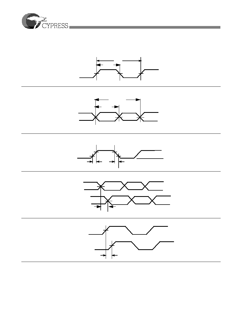
Switching Waveforms
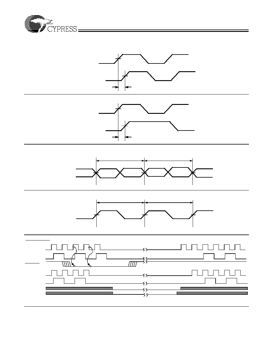
Duty Cycle Timing
t
1A
t
1B
(Single Ended Output)
Duty Cycle Timing (CPU Differential Output)
t
1A
t
1B
All Outputs Rise/Fall Time
OUTPUT
t
2
V
OH
0V
t
3
CPU-CPU Clock Skew
Host_b
Host
Host_b
Host
t
4
3V66-3V66 Clock Skew
3V66
3V66
t
5
CY2220
Document #: 38-07206 Rev. *A
Page 7 of 11
Note:
8.
Shaded section on the VCO and Crystal waveforms indicates that the VCO and crystal oscillator are active, and there is a valid clock.
Switching Waveforms
(continued)
PCI-PCI Clock Skew
PCI
PCI
t
6
3V66
PCI
t
7
3V66-PCI Clock Skew
Host
t
8A
t
8B
Host_b
CPU Clock Cycle-Cycle Jitter
CLK
t
9A
t
9B
Cycle-Cycle Clock Jitter
PWR_DOWN
[8]
CPUCLK
(Internal)
PCICLK
(Internal)
PWR_DWN
PCICLK
CPUCLK
(External)
(External)
VCO
Crystal
CY2220
Document #: 38-07206 Rev. *A
Page 8 of 11
Notes:
9.
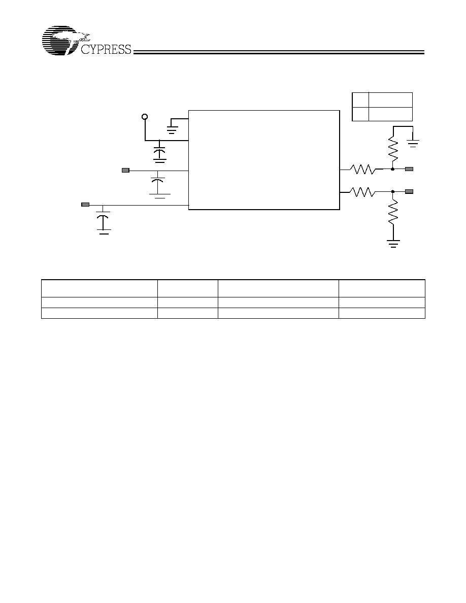
Each supply pin must have an individual decoupling capacitor.
10. All capacitors must be placed as close to the pins as is physically possible.
Test Circuit
[9, 10]
1, 7, 13, 19, 24, 32, 33, 37, 40, 46, 53
4, 10, 16, 22, 27, 29, 36, 38, 43, 49, 56
V
DDPCI
, V
DD3V66
,
OUTPUTS
CY2220
V
DDUSB
, V
DDREF
,
AV
DD,
V
DDCPU
,
Test
Nodes
R
s
R
s
R
p
R
p
V
DDMRef
CPU
Ref, USB Outputs
PCI, 3V66, MRef Outputs
30 pF
20 pF
Test Node
Test Node
Rs
Rp
33.2
49.9
Ordering Information
Ordering Code
Package
Name
Package Type
Operating
Range
CY2220PVC-1
O56
56-Pin SSOP
Commercial
CY2220PVC-2
O56
56-Pin SSOP
Commercial

CY2220
Document #: 38-07206 Rev. *A
Page 9 of 11
Layout Example
56
55
54
53
52
51
50
49
48
47
46
45
44
43
42
6
7
13
19
20
24
G = VIA to GND plane layer V =VIA to respective supply plane layer
Note: Each supply plane or strip should have a ferrite bead and capacitors
G
1
2
3
4
5
8
9
11
12
14
15
16
17
22
23
21
25
26
27
28
40
39
18
41
10
31
30
29
36
35
34
33
32
37
38
G
V
FB
+3.3V Supply
C4
Cermaic Caps C3 = 10≠22 µF
C4 = 0.005 µF
10
µ
F
FB = Dale ILB1206 - 300 (30
@ 100 MHz)
0.005
µ
F
G
G
C3
G
V
All bypass caps = 0.01
µ
F ceramic
G
V
G
V
G
V
G
V
G
V
G
V
G
V
G
V
VDDQ3
CY2220
CY2220
Document #: 38-07206 Rev. *A
Page 10 of 11
© Cypress Semiconductor Corporation, 2001. The information contained herein is subject to change without notice. Cypress Semiconductor Corporation assumes no responsibility for the use
of any circuitry other than circuitry embodied in a Cypress Semiconductor product. Nor does it convey or imply any license under patent or other rights. Cypress Semiconductor does not authorize
its products for use as critical components in life-support systems where a malfunction or failure may reasonably be expected to result in significant injury to the user. The inclusion of Cypress
Semiconductor products in life-support systems application implies that the manufacturer assumes all risk of such use and in doing so indemnifies Cypress Semiconductor against all charges.
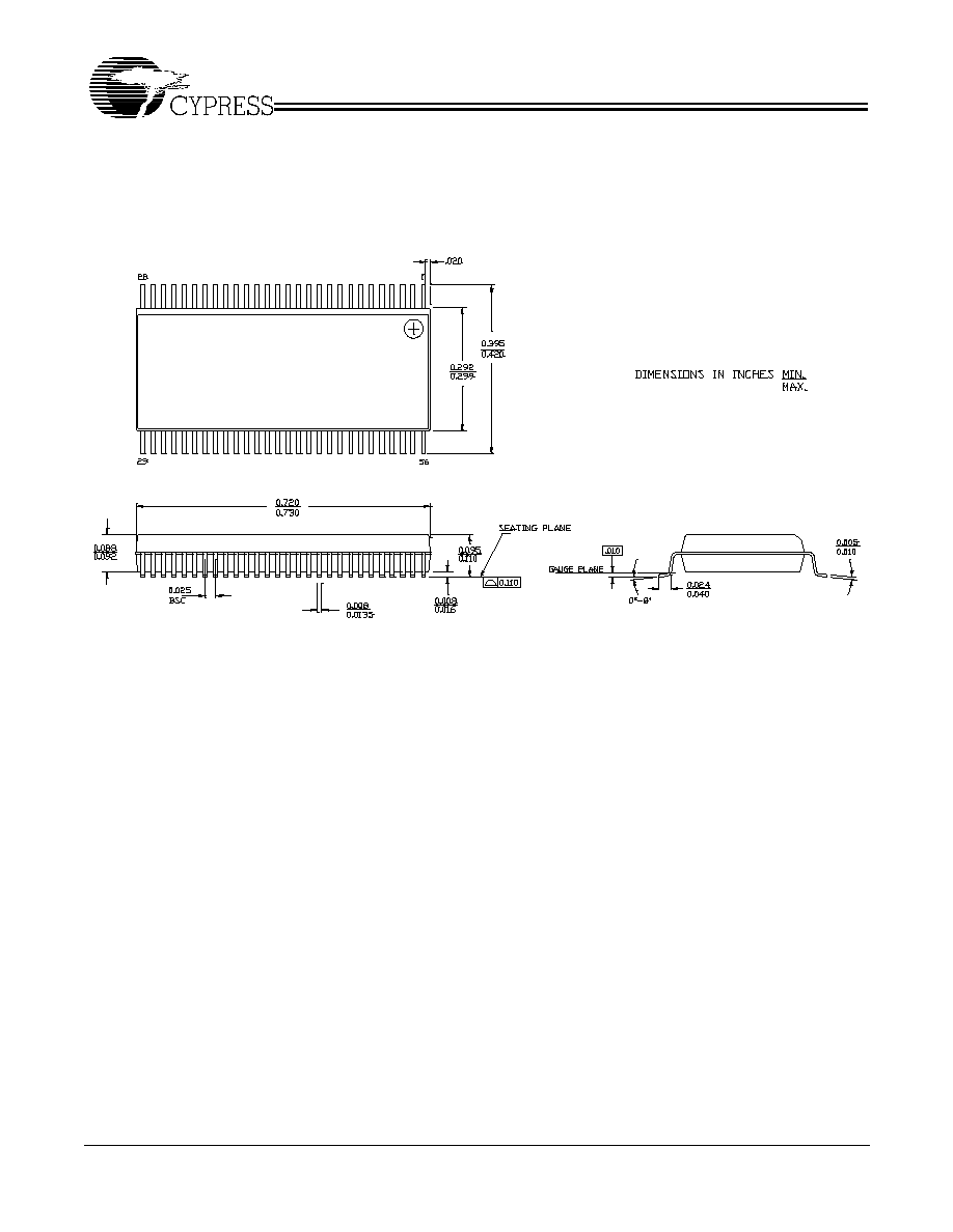
Package Diagram
56-Lead Shrunk Small Outline Package O56
51-85062-*C

CY2220
Document #: 38-07206 Rev. *A
Page 11 of 11
Document Title: CY2220 133-MHz Spread Spectrum Clock Synthesizer/Driver with Differential CPU Outputs
Document Number: 38-07206
REV.
ECN NO.
Issue
Date
Orig. of
Change
Description of Change
**
111730
01/17/02
DSG
Change from Spec number: 38-00813 to 38-07206
*A
121841
12/30/02
RBI
Power up requirements added to Operating Conditions Information