
Pentium
/II Clock Synthesizer/Driver for Mobile PCs
with Intel
82430TX and No SDRAM
CY2278A
Cypress Semiconductor Corporation
∑
3901 North First Street
∑
San Jose
∑
CA 95134
∑
408-943-2600
Document #: 38-07211 Rev. *A
Revised Decemeber 07, 2002
8A
Features
∑ Mixed 2.5V and 3.3V operation
∑ Complete clock solution to meet requirements of mo-
bile Pentium
Æ
and Pentium
Æ
II motherboards
-- Seven CPU clock outputs (three at 3.3V, and four at
2.5V or 3.3V) with eight selectable clock frequencies.
-- Ten 3.3V synchronous PCI clock outputs
-- Two 3.3V USB/IR clocks at 48 MHz
-- One Keyboard clock at 8 MHz
-- One 2.5V IOAPIC clock at 14.318 MHz
-- Two 3.3V Ref. clocks at 14.318 MHz
∑ Dedicated power management for portable systems
-- Separate output enable pins for CPU, PCI, and
USB/IR clock sets
-- Free-running PCI and CPU clocks (see options)
∑ Factory-EPROM programmable output drive and slew
rate for EMI customization
∑ Custom configuration with factory-EPROM program-
mable CPU, PCI, and USB/IR frequencies.
∑ Low skew and low jitter outputs
∑ Available in space-saving 48-pin TSSOP package
Functional Description
The CY2278A is a Clock Synthesizer/Driver chip for Pentium
or Pentium II portable PCs designed with the 82430TX or sim-
ilar core-logic chipsets. There are four options available as
shown in the selector guide.
The CY2278A outputs seven CPU clocks, three of which run
at 3.3V and four run at either 2.5V or 3.3V, depending on the
voltage applied on pin 42. There are ten PCI clocks, running
at one half the CPU clock frequency. Free-running PCI and
CPU clocks are available as options shown in the selector
guide. Additionally, the part outputs two 3.3V USB/IR clocks at
48 MHz, one Keyboard clock at 8 MHz, one 2.5V IOAPIC clock
at 14.318 MHz, and two 3.3V reference clocks at 14.318 MHz.
The CY2278 family contains several features for output flexi-
bility and power control. The CPU, PCI, USB and IR clock
frequencies are all factory EPROM-programmable. Three
hardware select inputs support eight CPU clock frequencies
from 20≠75 MHz. Additionally, each of the CPU, PCI, and
USB/IR clock sets can be turned on or off with a dedicated
enable input pin for power management.
The CY2278A outputs are designed for low EMI emissions.
Controlled rise and fall times, unique output driver circuits and
factory-EPROM programmable output drive and slew-rate en-
able optimal configurations for EMI control.
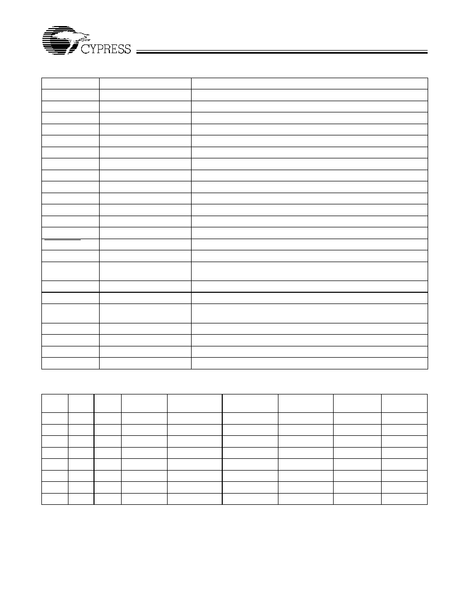
CY2278A Selector Guide
Notes:
1.
One free-running CPU clock.
2.
Two free-running PCI clocks.
Clock Outputs
-1L
-2L
-3L
-4L
CPU@3.3V
3
3
3
3
CPU@2.5/3.3V
4
[1]
4
4
4
PCI (CPU/2 MHz)
10
[2]
10
10
[2]
10
[2]
USB/IR (48 MHz)
2
2
2
2
KB (8 MHz)
1
1
1
1
IOAPIC (14.318 MHz)
2
2
2
2
Ref (14.318 MHz)
2
2
2
2
CPU-PCI delay
0 ns
0 ns
1≠5 ns
0 ns
Intel and Pentium are registered trademarks of Intel Corporation.
EPROM
Logic Block Diagram
X
OUT
X
IN
IOAPIC
OSC.
CLK8MHz
SEL2
XCPUCLK3_F
PLL0
USB_RUN
PLL1
/2
CPU_RUN
PCI_RUN
REF[0-1]
2.5≠3.3V Driver
USBCLK/IRCLK
XCPUCLK [0-2]
CPUCLK [0-2]
PCICLK [2-9]
SEL1
SEL0
2.5≠3.3V Driver
14.318 MHz
96 MHz
48 MHz
8 MHZ
D
CK
CPUCLK
PCICLK
/2
/12
D
CK
D
CK
PCICLK_F [0-1]
D
CK
D
CK
D
CK
on -1L only; not free-
running on -2L, -3L, -4L
running on -2L
on -1L, -3L, -4L only; not free-

CY2278A
Document #: 38-07211 Rev. *A
Page 2 of 12
Pin Configurations
1
2
3
4
5
6
7
8
9
10
11
12
33
32
31
30
29
25
26
27
28
36
35
REF1
34
TSSOP
Top View
13
14
15
16
17
18
19
20
21
22
23
24
45
44
43
42
41
37
38
39
40
48
47
46
2278A-1L
REF0
V
SS
X
IN
X
OUT
V
DDQ3
PCICLK0_F
PCICLK1_F
V
SS
PCICLK2
PCICLK3
PCICLK4
PCICLK5
V
DDQ3
PCICLK6
V
SS
PCICLK7
PCICLK8
V
DDQ3
PCICLK9
CLK8MHz
V
DDQ3
USBCLK
IRCLK
V
DDQ2
IOAPIC
PWR_DWN
V
SS
XCPUCLK0
XCPUCLK1
V
DDCPU
XCPUCLK2
XCPUCLK3_F
V
SS
CPUCLK0
CPUCLK1
V
DDQ3
CPUCLK2
SEL0
V
SS
SEL1
SEL2
V
SS
CPU_RUN
USB_RUN
PCI_RUN
AV
DD
V
SS
1
2
3
4
5
6
7
8
9
10
11
12
33
32
31
30
29
25
26
27
28
36
35
REF1
34
TSSOP
Top View
13
14
15
16
17
18
19
20
21
22
23
24
45
44
43
42
41
37
38
39
40
48
47
46
2278A-2L
REF0
V
SS
X
IN
X
OUT
V
DDQ3
PCICLK0
PCICLK1
V
SS
PCICLK2
PCICLK3
PCICLK4
PCICLK5
V
DDQ3
PCICLK6
V
SS
PCICLK7
PCICLK8
V
DDQ3
PCICLK9
CLK8MHz
V
DDQ3
USBCLK
IRCLK
V
DDQ2
IOAPIC
PWR_DWN
V
SS
XCPUCLK0
XCPUCLK1
V
DDCPU
XCPUCLK2
XCPUCLK3
V
SS
CPUCLK0
CPUCLK1
V
DDQ3
CPUCLK2
SEL0
V
SS
SEL1
SEL2
V
SS
CPU_RUN
USB_RUN
PCI_RUN
AV
DD
V
SS
1
2
3
4
5
6
7
8
9
10
11
12
33
32
31
30
29
25
26
27
28
36
35
REF1
34
TSSOP
Top View
13
14
15
16
17
18
19
20
21
22
23
24
45
44
43
42
41
37
38
39
40
48
47
46
2278A-3L
REF0
V
SS
X
IN
X
OUT
V
DDQ3
PCICLK0_F
PCICLK1_F
V
SS
PCICLK2
PCICLK3
PCICLK4
PCICLK5
V
DDQ3
PCICLK6
V
SS
PCICLK7
PCICLK8
V
DDQ3
PCICLK9
CLK8MHz
V
DDQ3
USBCLK
IRCLK
V
DDQ2
IOAPIC
PWR_DWN
V
SS
XCPUCLK0
XCPUCLK1
V
DDCPU
XCPUCLK2
XCPUCLK3
V
SS
CPUCLK0
CPUCLK1
V
DDQ3
CPUCLK2
SEL0
V
SS
SEL1
SEL2
V
SS
CPU_RUN
USB_RUN
PCI_RUN
AV
DD
V
SS
1
2
3
4
5
6
7
8
9
10
11
12
33
32
31
30
29
25
26
27
28
36
35
REF1
34
TSSOP
Top View
13
14
15
16
17
18
19
20
21
22
23
24
45
44
43
42
41
37
38
39
40
48
47
46
2278A-4L
REF0
V
SS
X
IN
X
OUT
V
DDQ3
PCICLK0_F
PCICLK1_F
V
SS
PCICLK2
PCICLK3
PCICLK4
PCICLK5
V
DDQ3
PCICLK6
V
SS
PCICLK7
PCICLK8
V
DDQ3
PCICLK9
CLK8MHz
V
DDQ3
USBCLK
IRCLK
V
DDQ2
IOAPIC
PWR_DWN
V
SS
XCPUCLK0
XCPUCLK1
V
DDCPU
XCPUCLK2
XCPUCLK3
V
SS
CPUCLK0
CPUCLK1
V
DDQ3
CPUCLK2
SEL0
V
SS
SEL1
SEL2
V
SS
CPU_RUN
USB_RUN
PCI_RUN
AV
DD
V
SS
CY2278A
Document #: 38-07211 Rev. *A
Page 3 of 12
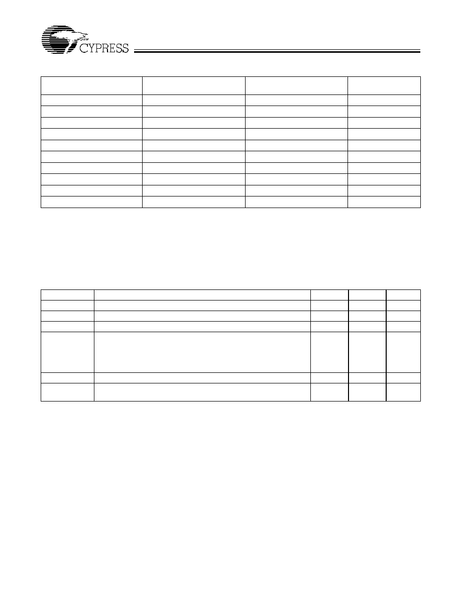
Pin Summary
Name
Pins
Description
V
DDQ3
6, 14, 19, 22, 36
3.3V Digital voltage supply
V
DDQ2
48
IOAPIC Digital voltage supply, 2.5V
V
DDCPU
42
CPU Digital voltage supply, 2.5V or 3.3V
AV
DD
26
Analog voltage supply, 3.3V
V
SS
3, 9, 16, 25, 31, 33, 39, 45
Ground
XTALIN
[3]
4
Reference crystal input
XTALOUT
[3]
5
Reference crystal feedback
SEL2
30
CPU clock frequency select input, bit 2
SEL1
32
CPU clock frequency select input, bit 1
SEL0
34
CPU clock frequency select input, bit 0
PCI_RUN
27
Control input, stops all PCI clocks except PCICLK_F when driven LOW
USB_RUN
28
Control input, stops all USB/IR clocks when driven LOW
CPU_RUN
29
Control input, stops all CPU clocks except XCPUCLK_F when driven LOW
PWR_DWN
46
Power down input, shuts down device when driven LOW
XCPUCLK[0:2]
44, 43, 41
2.5V or 3.3V CPU clock outputs
XCPUCLK3_F
40
2.5V or 3.3V CPU clock output, free-running on CY2278A-1L only. This output
is not free-running on the -2L, -3L, -4L configurations.
CPUCLK[0:2]
38, 37, 35
3.3V CPU clock output
PCICLK[2:9]
10, 11, 12, 13, 15, 17, 18, 20 PCI clock outputs
PCICLK_F[0:1]
7, 8
PCI clock outputs, free-running on CY2278A-1L, -3L, -4L only. This output is
not free-running on the -2L configuration
CLK8MHZ
21
8-MHz Keyboard clock output
IOAPIC
47
IOAPIC clock output
REF[0:1]
2, 1
Reference clock outputs, 14.318 MHz. REF0 has high drive
USBCLK/IRCLK
23, 24
USB or IR clock outputs, 48 MHz
Function Table
SEL2
SEL1
SEL0
XTALIN
CPUCLK
PCICLK
REF
IOAPIC
USBCLK
IRCLK
CLK8MHZ
0
0
0
14.318 MHz
75.0 MHz
37.5 MHz
14.318 MHz
48.0 MHz
8.0 MHz
0
0
1
14.318 MHz
20.0 MHz
10.0 MHz
14.318 MHz
48.0 MHz
8.0 MHz
0
1
0
14.318 MHz
25 MHz
12.5 MHz
14.318 MHz
48.0 MHz
8.0 MHz
0
1
1
14.318 MHz
33.33 MHz
16.67 MHz
14.318 MHz
48.0 MHz
8.0 MHz
1
0
0
14.318 MHz
50.0 MHz
25.0 MHz
14.318 MHz
48.0 MHz
8.0 MHz
1
0
1
14.318 MHz
60.0 MHz
30.0 MHz
14.318 MHz
48.0 MHz
8.0 MHz
1
1
0
14.318 MHz
66.67 MHz
33.33 MHz
14.318 MHz
48.0 MHz
8.0 MHz
1
1
1
14.318 MHz
40.0 MHz
20.0 MHz
14.318 MHz
48.0 MHz
8.0 MHz
Note:
3.
For best accuracy, use a parallel-resonant crystal, C
LOAD
= 18 pF.
CY2278A
Document #: 38-07211 Rev. *A
Page 4 of 12
Maximum Ratings
(Above which the useful life may be impaired. For user guide-
lines, not tested.)
Supply Voltage ..................................................≠0.5 to +7.0V
Input Voltage .............................................. ≠0.5V to V
DD
+0.5
Storage Temperature (Non-Condensing) ... ≠65
∞
C to +150
∞
C
Junction Temperature ............................................... +150
∞
C
Package Power Dissipation.............................................. 1W
Static Discharge Voltage............................................ >2000V
(per MIL-STD-883, Method 3015, like V
DD
pins tied together)
Actual Clock Frequency Values
Clock Output
Target Frequency
(MHz)
Actual Frequency
(MHz)
PPM
CPUCLK(0,0,0)
75.0
75.0
0
CPUCLK(0,0,1)
20.0
19.979
≠1057
CPUCLK(0,1,0)
25
24.974
≠1057
CPUCLK(0,1,1)
33.33
33.298
≠1107
CPUCLK(1,0,0)
50.0
49.947
≠1057
CPUCLK(1,0,1)
60.0
60.0
0
CPUCLK(1,1,0)
66.67
66.654
≠171
CPUCLK(1,1,1)
40.0
39.992
≠196
USBCLK
[4]
48.0
48.008
167
CLK8MHz
8.0
8.001
167
Operating Conditions
[5]
Parameter
Description
Min.
Max.
Unit
AV
DD
, V
DDQ3
Analog and Digital Supply Voltage
3.135
3.465
V
V
DDCPU,
V
DDQ2
CPU and IOAPIC Supply Voltage
2.375
2.625
V
T
A
Operating Temperature, Ambient
0
70
∞
C
C
L
Max. Capacitive Load on
XCPUCLK, CPUCLK, USBCLK/IRCLK, CLK8MHZ, REF1,
IOAPIC
PCICLK
REF0
20
20
30
45
pF
f
(REF)
Reference Frequency, Oscillator Nominal Value
14.318
14.318
MHz
t
PU
Power-up time for all VDD's to reach minimum specified voltage (power
ramps must be monotonic)
0.05
50
ms
Notes:
4.
Meets Intel USB clock requirements.
5.
Electrical parameters are guaranteed with these operating conditions.

CY2278A
Document #: 38-07211 Rev. *A
Page 5 of 12
Electrical Characteristics
Parameter
Description
Test Conditions
Min. Max. Unit
V
IH
High-level Input Voltage
Except Crystal Inputs
[6]
2.0
V
V
IL
Low-level Input Voltage
Except Crystal Inputs
[6]
0.8
V
V
OH
High-level Output Volt-
age
V
DDCPU
, V
DDQ2
= 2.375V
I
OH
= 9 mA
XCPUCLK
2.0
V
I
OH
= 13 mA IOAPIC
V
OL
Low-level Output Voltage V
DDCPU
, V
DDQ2
= 2.375V
I
OL
= 13 mA
XCPUCLK
0.4
V
I
OL
= 18 mA
IOAPIC
V
OH
High-level Output Volt-
age
V
DDQ3
, AV
DD
, V
DDCPU
= 3.135V
I
OH
= 23 mA XCPUCLK
2.4
V
I
OH
= 23 mA CPUCLK
I
OH
= 23 mA PCICLK
I
OH
= 23 mA USBCLK
I
OH
= 23 mA CLK8MHZ
I
OH
= 23 mA REF0
I
OH
= 23 mA REF1
V
OL
Low-level Output Voltage V
DDQ3
, AV
DD
, V
DDCPU
= 3.135V
I
OL
= 17 mA
XCPUCLK
0.4
V
I
OL
=17 mA
CPUCLK
I
OL
= 17 mA
PCICLK
I
OL
= 17 mA
USBCLK
I
OL
= 17 mA
CLK8MHZ
I
OL
= 17 mA
REF0
I
OL
= 17 mA
REF1
I
IH
Input High Current
V
IH
= V
DD
≠10
+10
µ
A
I
IL
Input Low Current
V
IL
= 0V
10
µ
A
I
DD
Power Supply Current
[7]
V
DDQ3
= 3.465V, V
IN
= 0 or V
DD
, Loaded Outputs,
CPU clocks = 66.67 MHz
200
mA
I
DD
Power Supply Current
[7]
V
DDQ3
= 3.465V, V
IN
= 0 or V
DD
, Unloaded Outputs
100
mA
I
DDS
Power-down Current
Current draw in power-down state
150
µ
A
Notes:
6.
Crystal inputs have CMOS thresholds.
7.
Power supply current will vary with number of outputs which are running. Therefore, power supply current can be calculated with the following formula: to be
determined.