 | –≠–ª–µ–∫—Ç—Ä–æ–Ω–Ω—ã–π –∫–æ–º–ø–æ–Ω–µ–Ω—Ç: CY2303SI | –°–∫–∞—á–∞—Ç—å:  PDF PDF  ZIP ZIP |
Phase-Aligned Clock Multiplier
CY2303
Cypress Semiconductor Corporation
∑
3901 North First Street
∑
San Jose
∑
CA 95134
∑
408-943-2600
Document #: 38-07249 Rev. *A
Revised December 7, 2002
3
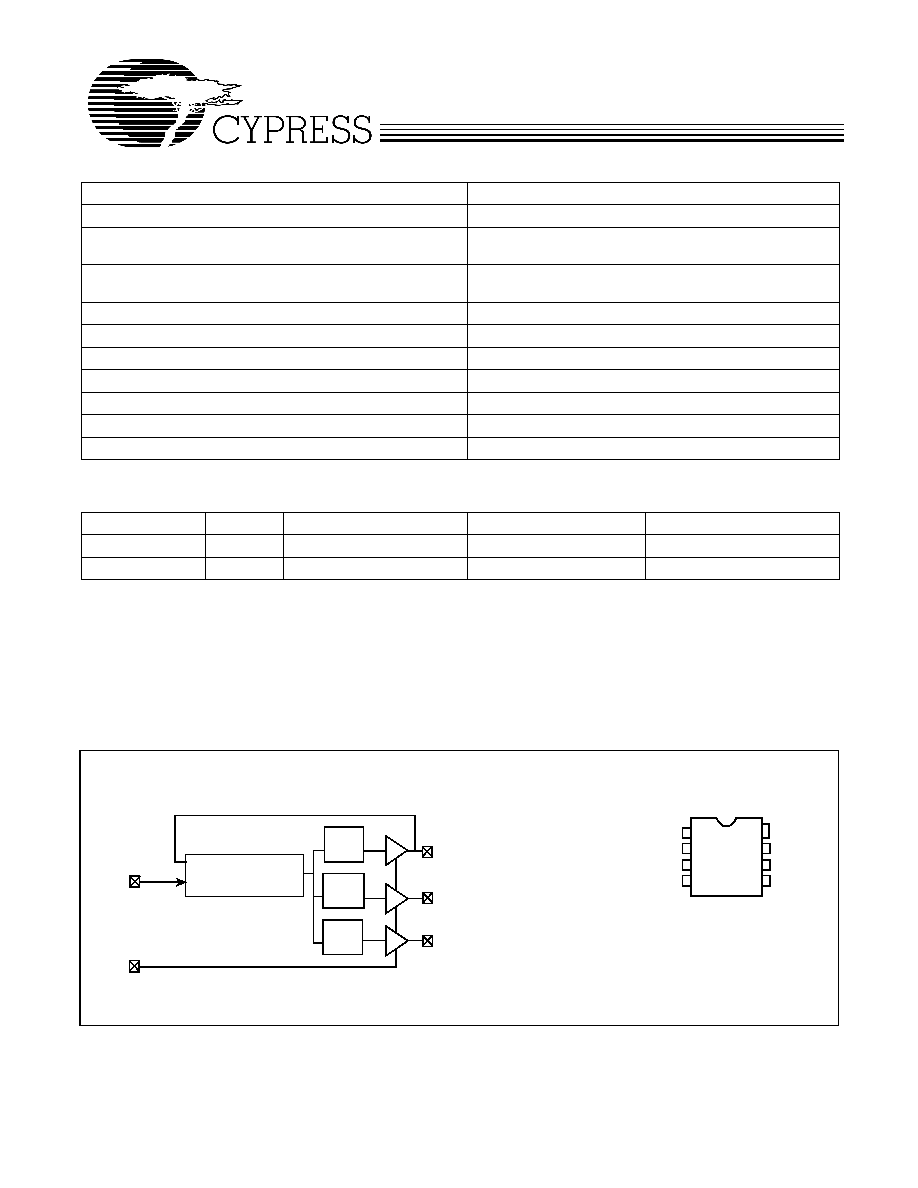
Functional Description
The CY2303 is a 3 output 3.3V phase-aligned system clock
designed to distribute high-speed clocks in PC, workstation,
datacom, telecom, and other high-performance applications.
The part allows user to obtain 1x, 2x, and 4x Ref output fre-
quencies on respective output pins.
The CY2303 has an on-chip PLL which locks to an input clock
presented on the REFIN pin. The PLL feedback is internally
connected to the REF output. The input-to-output skew is
guaranteed to be less than
±
200 ps, and output-to-output skew
is guaranteed to be less than 200 ps.
Multiple CY2303 devices can accept the same input clock and
distribute it in a system. In this case, the skew between the
outputs of two devices is guaranteed to be less than 400 ps.
The CY2303 is available in commercial and industrial temper-
ature ranges.
Features
Benefits
∑ 3-multiplier configuration
1x, 2x, 4x Ref
∑ Single phase-locked loop architecture
10 MHz to 166.67 MHz operating range (reference input from
10 MHz to 41.67 MHz)
∑ Phase Alignment
All outputs will have a consistent phase relationship with each
other and the reference input
∑ Low jitter, high accuracy outputs
Meets critical timing requirements
∑ Output enable pin
Enables design flexibility and lower power consumption
∑ 3.3V operation
Supports industry standard design platforms
∑ 5V Tolerant input
Allows flexibility on Reference input
∑ Sophisticated internal loop filter
Alleviates the need for external components
∑ 8-pin 150-mil SOIC package
Industry standard packaging saves on board space
∑ Commercial and Industrial Temperature available
Suitable for wide spectrum of applications
Selector Guide
Part Number
Outputs
Input Frequency Range
Output Frequency Range
Specifics
CY2303SC
3
10 MHz≠41.67 MHz
10 MHz≠166.67 MHz
Commercial Temperature
CY2303SI
3
10 MHz≠41.67 MHz
10 MHz≠166.67 MHz
Industrial Temperature
PLL
REF
REFx2
REFx4
OE
x1
x2
x4
1
2
3
4
5
8
7
6
REF
GND
REFIN
N/C
V
DD
OE
REFx2
Top View
8-pin SOIC
REFx4
REFIN
Block Diagram
Pin Configuration
FBK

CY2303
Document #: 38-07249 Rev. *A
Page 2 of 7
Maximum Ratings
Supply Voltage to Ground Potential ............... ≠0.5V to +7.0V
DC Input Voltage (Except Ref)...............≠0.5V to V
DD
+ 0.5V
DC Input Voltage REFIN ........................................≠0.5 to 7V
Storage Temperature ................................. ≠65∞C to +150∞C
Junction Temperature .................................................. 150∞C
Static Discharge Voltage
(per MIL-STD-883, Method 3015) ............................. >2000V
Pin Description
Pin
Signal
[1]
Description
1
REF
REF output (1x Reference input)
2
GND
Ground
3
REFIN
Input reference frequency, 5V tolerant input
4
N/C
No Connect
5
REFx2
2x Reference input
6
REFx4
4x Reference input
7
VDD
3.3V Supply
8
OE
Output Enable (weak pull-up)
Operating Conditions for CY2303SC Commercial Temperature Devices
Parameter
Description
Min.
Max.
Unit
V
DD
Supply Voltage
3.0
3.6
V
T
A
Operating Temperature (Ambient Temperature)
0
70
∞C
C
L
Load Capacitance, Fout < 133.33 MHz
18
pF
Load Capacitance, 133.33 MHz < Fout < 166.67 MHz
12
pF
C
IN
Input Capacitance
7
pF
t
PU
Power-up time for all VDD's to reach minimum specified voltage
(power ramps must be monotonic)
0.05
50
ms
Electrical Characteristics for CY2303SC Commercial Temperature Devices
Parameter
Description
Test Conditions
Min.
Max.
Unit
V
IL
Input LOW Voltage
0.8
V
V
IH
Input HIGH Voltage
2.0
V
I
IL
Input LOW Current
V
IN
= 0V
100
µ
A
I
IH
Input HIGH Current
V
IN
= V
DD
50
µ
A
V
OL
Output LOW Voltage
[2]
I
OL
= 8 mA
0.4
V
V
OH
Output HIGH Voltage
[2]
I
OH
= ≠8 mA
2.4
V
I
DD
Supply Current
Unloaded outputs, REFIN = 41.67 MHz
45
mA
Unloaded outputs, REFIN = 25 MHz
32
mA
Unloaded outputs, REFIN = 10 MHz
18
mA
Notes:
1.
Weak pull-down on all outputs.
2.
Parameter is guaranteed by design and characterization. It is not 100% tested in production.
CY2303
Document #: 38-07249 Rev. *A
Page 3 of 7
Switching Characteristics for CY2303SC Commercial Temperature Devices
Parameter
Name
Test Conditions
Min.
Typ.
Max.
Unit
1/t
1
Output Frequency
18-pF load
10
133.33
MHz
12-pF load
166.67
MHz
Duty Cycle
[3]
= t
2
˜
t
1
Measured at V
DD
/2
40
50
60
%
t
3
Rise Time
[3]
Measured between 0.8V and 2.0V
1.20
ns
t
4
Fall Time
[3]
Measured between 0.8V and 2.0V
1.20
ns
t
5
Output to Output Skew on rising
edges
[3]
All outputs equally loaded
Measured at V
DD
/2
200
ps
t
6
Delay, REFIN Rising Edge to
REF Rising Edge
[3]
Measured at V
DD
/2 from REFIN to any out-
put
±
200
ps
t
7
Device to Device Skew
[3]
Measured at V
DD
/2 on the REF pin of the
device (pin 1)
400
ps
t
J
Period Jitter
[3]
Measured at Fout < 133.33 MHz, loaded
outputs, 18-pF load
±
175
ps
t
LOCK
PLL Lock Time
[3]
Stable power supply, valid clocks presented
on REFIN
1.0
ms
Operating Conditions for CY2303SI Industrial Temperature Devices
Parameter
Description
Min.
Max.
Unit
V
DD
Supply Voltage
3.0
3.6
V
T
A
Operating Temperature (Ambient Temperature)
≠40
85
∞C
C
L
Load Capacitance, Fout <133.33 MHz
15
pF
Load Capacitance, 133.33 MHz < Fout < 166.67 MHz,
10
pF
t
PU
Power-up time for all VDD's to reach minimum specified voltage
(power ramps must be monotonic)
0.05
50
ms
Electrical Characteristics for CY2303SI Industrial Temperature Devices
Parameter
Description
Test Conditions
Min.
Max.
Unit
V
IL
Input LOW Voltage
0.8
V
V
IH
Input HIGH Voltage
2.0
V
I
IL
Input LOW Current
V
IN
= 0V
100
µ
A
I
IH
Input HIGH Current
V
IN
= V
DD
50
µ
A
V
OL
Output LOW Voltage
[2]
I
OL
= 8 mA
0.4
V
V
OH
Output HIGH Voltage
[2]
I
OH
= ≠8 mA
2.4
V
I
DD
Supply Current
Unloaded outputs, REFIN = 41.67 MHz
48
mA
Unloaded outputs, REFIN = 25 MHz
35
mA
Unloaded outputs, REFIN = 10 MHz
20
mA
Note:
3.
All parameters are specified with loaded outputs.
CY2303
Document #: 38-07249 Rev. *A
Page 4 of 7
Switching Characteristics for CY2303SI Industrial Temperature Devices
Parameter
Name
Test Conditions
Min.
Typ.
Max.
Unit
1/t
1
Output Frequency
15-pF load
10
133.33
MHz
10-pF load
166.67
MHz
Duty Cycle
[3]
= t
2
˜
t
1
Measured at V
DD
/2
40
50
60
%
t
3
Rise Time
[3]
Measured between 0.8V and 2.0V
1.20
ns
t
4
Fall Time
[3]
Measured between 0.8V and 2.0V
1.20
ns
t
5
Output to Output Skew on ris-
ing edges
[3]
All outputs equally loaded
Measured at V
DD
/2
200
ps
t
6
Delay, REFIN Rising Edge to
REF Rising Edge
[3]
Measured at V
DD
/2 from REFIN to any
output
±
200
ps
t
7
Device to Device Skew
[3]
Measured at V
DD
/2 on the REF pin of
the device (pin 1)
400
ps
t
J
Period Jitter
[3]
Measured at Fout < 133.33 MHz, loaded
outputs, 15-pF load
±
175
ps
t
LOCK
PLL Lock Time
[3]
Stable power supply, valid clocks pre-
sented on REFIN
1.0
ms
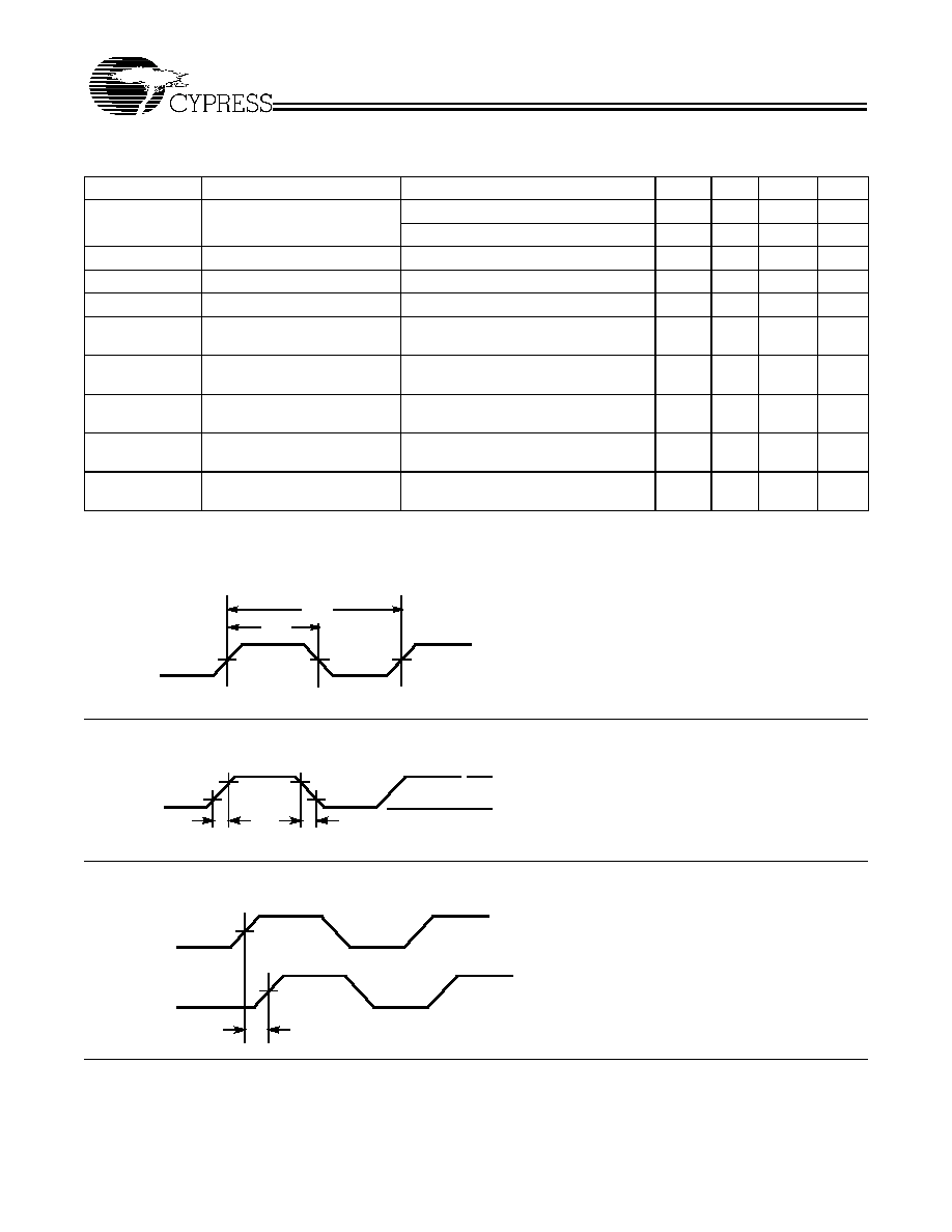
Switching Waveforms
Duty Cycle Timing
t
1
t
2
V
DD
/2
All Outputs Rise/Fall Time
OUTPUT
t
3
3.3V
0V
0.8V
2.0V
2.0V
0.8V
t
4
Output-Output Skew
V
DD
/2
t
5
OUTPUT
OUTPUT
V
DD
/2
CY2303
Document #: 38-07249 Rev. *A
Page 5 of 7
Test Circuits
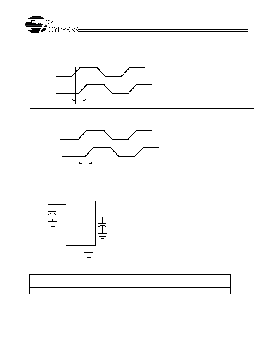
Switching Waveforms
Input-Output Propagation Delay
V
DD
/2
t
6
INPUT
FBK
V
DD
/2
V
DD
/2
t
7
FBK, Device 1
FBK, Device 2
Device-Device Skew
V
DD
/2
0.1
µ
F
V
DD
CLK
OUT
C
LOAD
OUTPUTS
GND
Test Circuit # 1
Ordering Information
Ordering Code
Package Name
Package Type
Operating Range
CY2303SC
S8
8-Pin 150-mil SOIC
Commercial
CY2303SI
S8
8-Pin 150-mil SOIC
Industrial
CY2303
Document #: 38-07249 Rev. *A
Page 6 of 7
© Cypress Semiconductor Corporation, 2001. The information contained herein is subject to change without notice. Cypress Semiconductor Corporation assumes no responsibility for the use
of any circuitry other than circuitry embodied in a Cypress Semiconductor product. Nor does it convey or imply any license under patent or other rights. Cypress Semiconductor does not authorize
its products for use as critical components in life-support systems where a malfunction or failure may reasonably be expected to result in significant injury to the user. The inclusion of Cypress
Semiconductor products in life-support systems application implies that the manufacturer assumes all risk of such use and in doing so indemnifies Cypress Semiconductor against all charges.
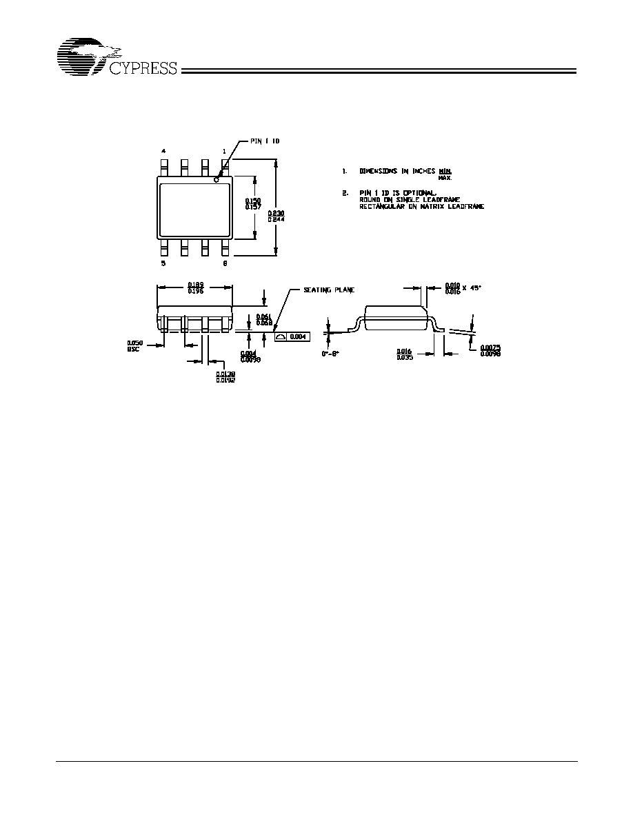
Package Diagram
8-Lead (150-Mil) SOIC S8
51-85066-A
51-85066-A

CY2303
Document #: 38-07249 Rev. *A
Page 7 of 7
Document Title: CY2303 Phase-Aligned Clock Multiplier
Document Number: 38-07249
REV.
ECN NO.
Issue
Date
Orig. of
Change
Description of Change
**
110514
01/07/02
SZV
Change from Spec number: 38-01036 to 38-07249
*A
121852
12/14/02
RBI
Power up requirements added to Operating Conditions Information