3.3V Zero Delay Buffer
CY2304
Cypress Semiconductor Corporation
∑
3901 North First Street
∑
San Jose
∑
CA 95134
∑
408-943-2600
Document #: 38-07247 Rev. *C
Revised December 7, 2002
Features
∑ Zero input-output propagation delay, adjustable by
capacitive load on FBK input
∑ Multiple configurations ≠ see "Available Configura-
tions" table
∑ Multiple low-skew outputs
-- Output-output skew less than 200 ps
-- Device-device skew less than 500 ps
∑ 10-MHz to 133-MHz operating range
∑ Low jitter, less than 200 ps cycle-cycle
∑ Space-saving 8-pin 150-mil SOIC package
∑ 3.3V operation
∑ Industrial temperature available
Functional Description
The CY2304 is a 3.3V zero delay buffer designed to distribute
high-speed clocks in PC, workstation, datacom, telecom, and
other high-performance applications.
The part has an on-chip phase-locked loop (PLL) that locks to
an input clock presented on the REF pin. The PLL feedback is
required to be driven into the FBK pin, and can be obtained
from one of the outputs. The input-to-output skew is
guaranteed to be less than 250 ps, and output-to-output skew
is guaranteed to be less than 200 ps.
The CY2304 has two banks of two outputs each.
The CY2304 PLL enters a power-down state when there are
no rising edges on the REF input. In this mode, all outputs are
three-stated and the PLL is turned off, resulting in less than
25
µ
A of current draw.
Multiple CY2304 devices can accept the same input clock and
distribute it in a system. In this case, the skew between the
outputs of two devices is guaranteed to be less than 500 ps.
The CY2304 is available in two different configurations, as
shown in the "Available Configurations" table. The CY2304≠1
is the base part, where the output frequencies equal the
reference if there is no counter in the feedback path.
The CY2304≠2 allows the user to obtain Ref and 1/2x or 2x
frequencies on each output bank. The exact configuration and
output frequencies depends on which output drives the
feedback pin.
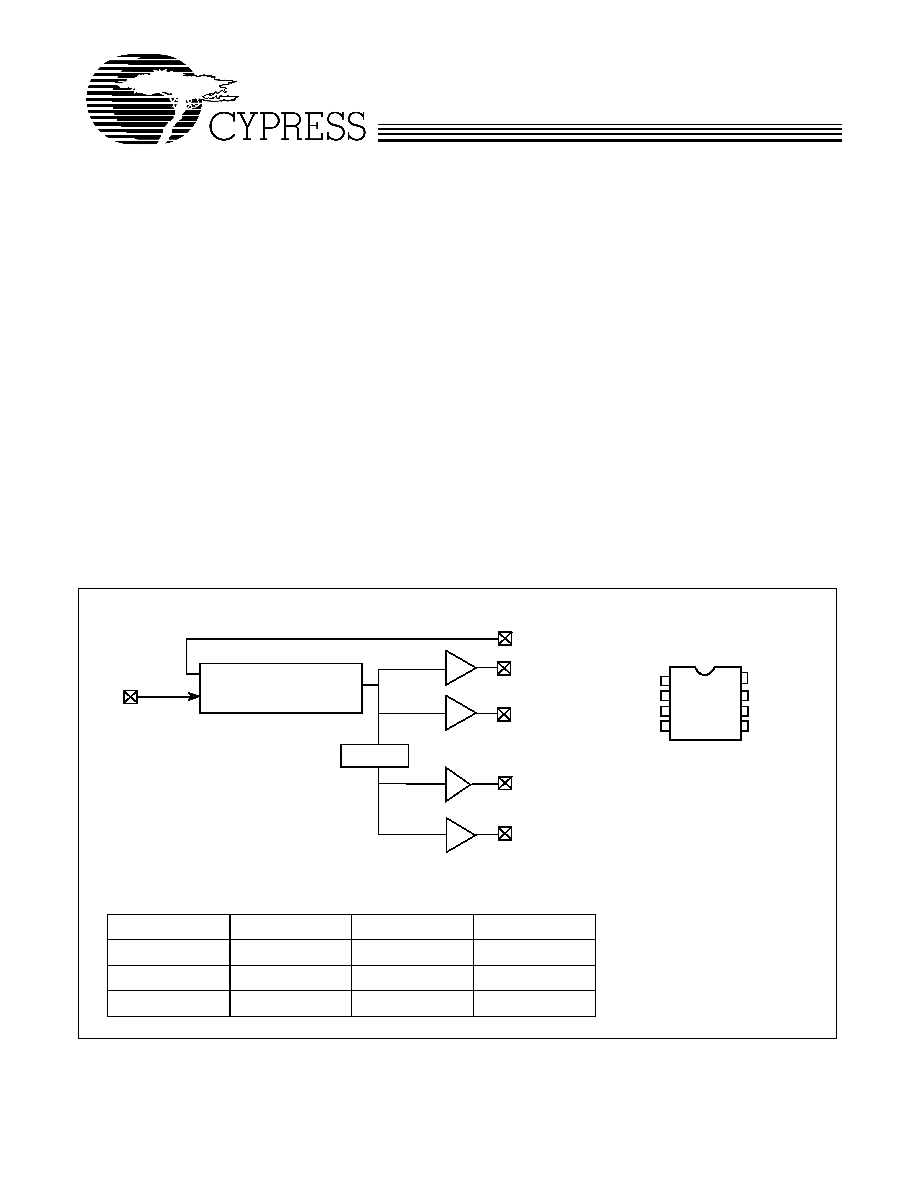
PLL
CLKA1
CLKA2
CLKB1
REF
CLKB2
/2
Extra Divider (-2)
Logic Block Diagram
1
2
3
4
5
8
7
6
REF
CLKA1
CLKA2
GND
V
DD
FBK
CLKB1
Top View
8-pin SOIC
Pin Configuration
CLKB2
FBK
Available Configurations
Device
FBK from
Bank A Frequency Bank B Frequency
CY2304-1
Bank A or B
Reference
Reference
CY2304-2
Bank A
Reference
Reference/2
CY2304-2
Bank B
2 ◊ Reference
Reference
CY2304
Document #: 38-07247 Rev. *C
Page 2 of 8
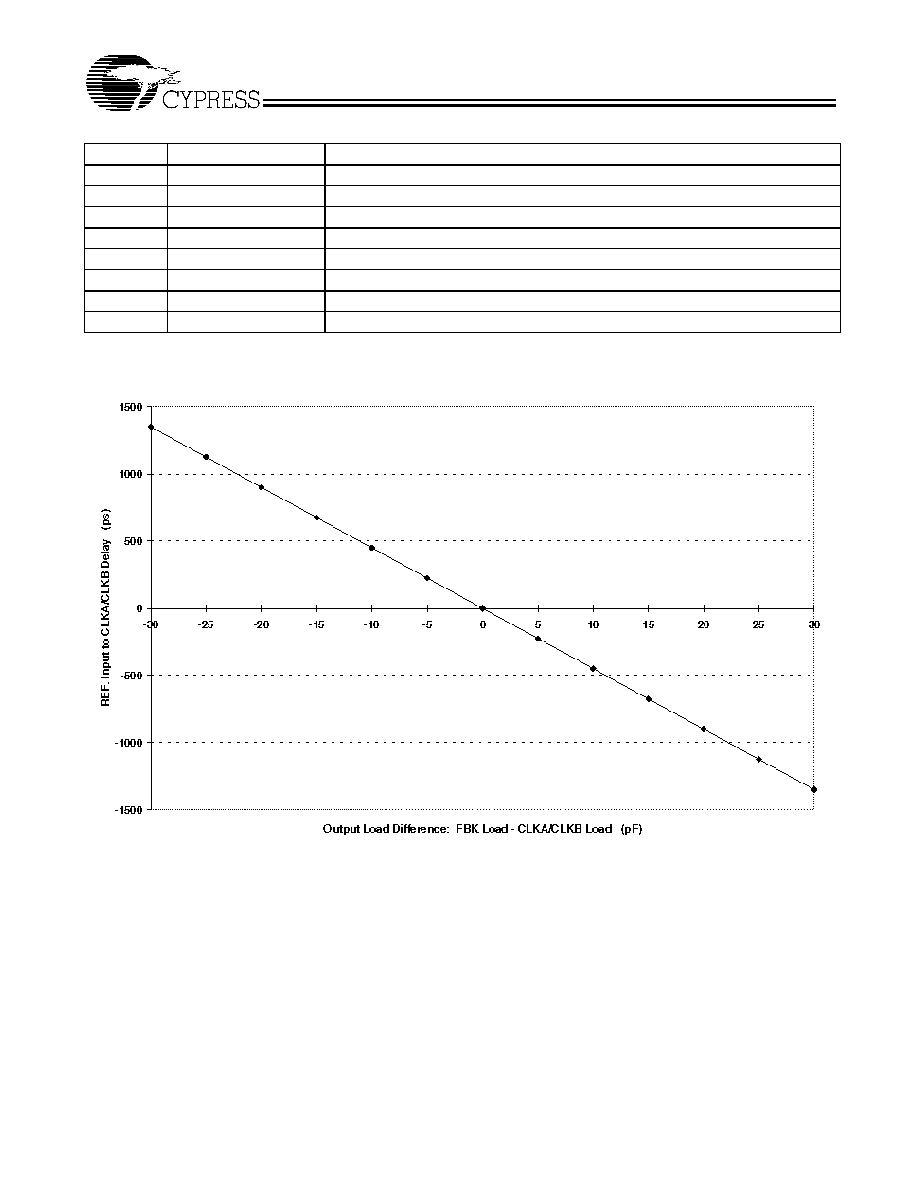
Zero Delay and Skew Control
To close the feedback loop of the CY2304, the FBK pin can be
driven from any of the four available output pins. The output
driving the FBK pin will be driving a total load of 7 pF plus any
additional load that it drives. The relative loading of this output
(with respect to the remaining outputs) can adjust the
input-output delay. This is shown in the graph above.
For applications requiring zero input-output delay, all outputs
including the one providing feedback should be equally
loaded. If input-output delay adjustments are required, use the
above graph to calculate loading differences between the
feedback output and remaining outputs.
For zero output-output skew, be sure to load outputs equally.
For further information on using CY2304, refer to the appli-
cation note "CY2308: Zero Delay Buffer."
Notes:
1.
Weak pull-down.
2.
Weak pull-down on all outputs.
Pin Description
Pin
Signal
Description
1
REF
[1]
Input reference frequency, 5V-tolerant input
2
CLKA1
[2]
Clock output, Bank A
3
CLKA2
[2]
Clock output, Bank A
4
GND
Ground
5
CLKB1
[2]
Clock output, Bank B
6
CLKB2
[2]
Clock output, Bank B
7
V
DD
3.3V supply
8
FBK
PLL feedback input
REF. Input to CLKA/CLKB Delay vs. Difference in Loading Between FBK Pin and CLKA/CLKB Pins
CY2304
Document #: 38-07247 Rev. *C
Page 3 of 8
Maximum Ratings
Supply Voltage to Ground Potential.................≠0.5V to +7.0V
DC Input Voltage (Except Ref) ...............≠0.5V to V
DD
+ 0.5V
DC Input Voltage REF.............................................≠0.5 to 7V
Storage Temperature ..................................≠65∞C to +150∞C
Junction Temperature ..................................................150∞C
Static Discharge Voltage
(per MIL-STD-883, Method 3015) .............................> 2000V
Operating Conditions for CY2304SC-X Commercial Temperature Devices
Parameter
Description
Min.
Max.
Unit
V
DD
Supply Voltage
3.0
3.6
V
T
A
Operating Temperature (Ambient Temperature)
0
70
∞C
C
L
Load Capacitance (below 100 MHz)
30
pF
Load Capacitance (from 100 MHz to 133 MHz)
15
pF
C
IN
Input Capacitance
[3]
7
pF
t
PU
Power-up time for all VDD's to reach minimum specified voltage
(power ramps must be monotonic)
0.05
50
ms
Electrical Characteristics for CY2304SC-X Commercial Temperature Devices
Parameter
Description
Test Conditions
Min.
Max.
Unit
V
IL
Input LOW Voltage
0.8
V
V
IH
Input HIGH Voltage
2.0
V
I
IL
Input LOW Current
V
IN
= 0V
50.0
µ
A
I
IH
Input HIGH Current
V
IN
= V
DD
100.0
µ
A
V
OL
Output LOW Voltage
[4]
I
OL
= 8 mA (≠1, ≠2)
0.4
V
V
OH
Output HIGH Voltage
[4]
I
OH
= ≠8 mA (≠1, ≠2)
2.4
V
I
DD
(PD mode)
Power-down Supply Current REF = 0 MHz
12.0
µ
A
I
DD
Supply Current
Unloaded outputs, 100-MHz REF,
Select inputs at V
DD
or GND
45.0
mA
Unloaded outputs, 66-MHz REF
(≠1,≠2)
32.0
mA
Unloaded outputs, 33-MHz REF
(≠1,≠2)
18.0
mA
Switching Characteristics for CY2304SC-X Commercial Temperature Devices
[5]
Parameter
Name
Test Conditions
Min.
Typ.
Max.
Unit
t
1
Output Frequency
30-pF load, all devices
10
100
MHz
t
1
Output Frequency
15-pF load, ≠1, ≠2 devices
10
133.3
MHz
Duty Cycle
[4]
= t
2
˜
t
1
(≠1,≠2)
Measured at 1.4V, F
OUT
= 66.66 MHz 30-pF load
40.0
50.0
60.0
%
Duty Cycle
[4]
= t
2
˜
t
1
(≠1,≠2)
Measured at 1.4V, F
OUT
< 50.0 MHz 15-pF load
45.0
50.0
55.0
%
t
3
Rise Time
[4]
(≠1, ≠2)
Measured between 0.8V and 2.0V, 30-pF load
2.20
ns
t
3
Rise Time
[4]
(≠1, ≠2)
Measured between 0.8V and 2.0V, 15-pF load
1.50
ns
Notes:
3.
Applies to both REF clock and FBK.
4.
Parameter is guaranteed by design and characterization. Not 100% tested in production.
5.
All parameters are specified with loaded output.
CY2304
Document #: 38-07247 Rev. *C
Page 4 of 8
t
4
Fall Time
[4]
(≠1, ≠2)
Measured between 0.8V and 2.0V,
30-pF load
2.20
ns
t
4
Fall Time
[4]
(≠1, ≠2)
Measured between 0.8V and 2.0V,
15-pF load
1.50
ns
t
5
Output-to-Output Skew
on same Bank (≠1,≠2)
[4]
All outputs equally loaded
200
ps
Output Bank A to Output
Bank B Skew (≠1)
All outputs equally loaded
200
ps
Output Bank A to Output
Bank B Skew (≠2)
All outputs equally loaded
400
ps
t
6
Skew, REF Rising Edge
to FBK Rising Edge
[4]
Measured at V
DD
/2
0
±
250
ps
t
7
Device-to-Device
Skew
[4]
Measured at V
DD
/2 on the FBK pins of devices
0
500
ps
t
J
Cycle-to-Cycle Jitter
[4]
(≠1)
Measured at 66.67 MHz, loaded outputs, 15-pF load
175
ps
Measured at 66.67 MHz, loaded outputs, 30-pF load
200
ps
Measured at 133.3 MHz, loaded outputs, 15 pF load
100
ps
t
J
Cycle-to-Cycle Jitter
[4]
(≠2)
Measured at 66.67 MHz, loaded outputs 30-pF load
400
ps
Measured at 66.67 MHz, loaded outputs 15-pF load
375
ps
t
LOCK
PLL Lock Time
[4]
Stable power supply, valid clocks presented on REF
and FBK pins
1.0
ms
Operating Conditions for CY2304SI-X Industrial Temperature Devices
Parameter
Description
Min.
Max.
Unit
V
DD
Supply Voltage
3.0
3.6
V
T
A
Operating Temperature (Ambient Temperature)
-40
85
∞C
C
L
Load Capacitance (below 100 MHz)
30
pF
Load Capacitance (from 100 MHz to 133 MHz)
15
pF
C
IN
Input Capacitance
7
pF
Switching Characteristics for CY2304SC-X Commercial Temperature Devices
(continued)
[5]
Parameter
Name
Test Conditions
Min.
Typ.
Max.
Unit
Switching Characteristics for CY2304SI-X Industrial Temperature Devices
[5]
Parameter
Name
Test Conditions
Min.
Typ.
Max.
Unit
t
1
Output Frequency
30-pF load, All devices
10
100
MHz
t
1
Output Frequency
15-pF load, All devices
10
133.3
MHz
Duty Cycle
[4]
= t
2
˜
t
1
(≠1,≠2)
Measured at 1.4V, F
OUT
= 66.66 MHz
30-pF load
40.0
50.0
60.0
%
Duty Cycle
[4]
= t
2
˜
t
1
(≠1,≠2)
Measured at 1.4V, F
OUT
< 50.0 MHz
15-pF load
45.0
50.0
55.0
%
t
3
Rise Time
[4]
(≠1, ≠2)
Measured between 0.8V and 2.0V,
30-pF load
2.50
ns
t
3
Rise Time
[4]
(≠1, ≠2)
Measured between 0.8V and 2.0V,
15-pF load
1.50
ns
t
4
Fall Time
[4]
(≠1, ≠2)
Measured between 0.8V and 2.0V,
30-pF load
2.50
ns
t
4
Fall Time
[4]
(≠1, ≠2)
Measured between 0.8V and 2.0V,
15-pF load
1.50
ns
CY2304
Document #: 38-07247 Rev. *C
Page 5 of 8
t
5
Output-to-Output Skew on
same Bank (≠1,≠2)
[4]
All outputs equally loaded
200
ps
Output Bank A to Output Bank
B Skew (≠1)
All outputs equally loaded
200
ps
Output Bank A to Output Bank
B Skew (≠2)
All outputs equally loaded
400
ps
t
6
Skew, REF Rising Edge to
FBK Rising Edge
[4]
Measured at V
DD
/2
0
±
250
ps
t
7
Device-to-Device Skew
[4]
Measured at V
DD
/2 on the FBK pins of
devices
0
500
ps
t
J
Cycle-to-Cycle Jitter
[4]
(≠1)
Measured at 66.67 MHz, loaded outputs,
15-pF load
180
ps
Measured at 66.67 MHz, loaded outputs,
30-pF load
200
ps
Measured at 133.3 MHz, loaded outputs,
15 pF load
100
ps
t
J
Cycle-to-Cycle Jitter
[4]
(≠2)
Measured at 66.67 MHz, loaded outputs,
30-pF load
400
ps
Measured at 66.67 MHz, loaded outputs,
15-pF load
380
ps
t
LOCK
PLL Lock Time
[4]
Stable power supply, valid clocks
presented on REF and FBK pins
1.0
ms
Electrical Characteristics for CY2304SI-X Industrial Temperature Devices
Parameter
Description
Test Conditions
Min.
Max.
Unit
V
IL
Input LOW Voltage
0.8
V
V
IH
Input HIGH Voltage
2.0
V
I
IL
Input LOW Current
V
IN
= 0V
50.0
µ
A
I
IH
Input HIGH Current
V
IN
= V
DD
100.0
µ
A
V
OL
Output LOW Voltage
[4]
I
OL
= 8 mA (≠1, ≠2)
0.4
V
V
OH
Output HIGH Voltage
[4]
I
OH
= ≠8 mA (≠1, ≠2)
2.4
V
I
DD
(PD mode)
Power-down Supply Current
REF = 0 MHz
25.0
µ
A
I
DD
Supply Current
Unloaded outputs, 100 MHz,
Select inputs at V
DD
or GND
45.0
mA
Unloaded outputs, 66-MHz REF
(≠1, ≠2)
35.0
mA
Unloaded outputs, 33-MHz REF
(≠1, ≠2)
20.0
mA
Switching Waveforms
Switching Characteristics for CY2304SI-X Industrial Temperature Devices
(continued)
[5]
Parameter
Name
Test Conditions
Min.
Typ.
Max.
Unit
Duty Cycle Timing
t
1
t
2
1.4V
1.4V
1.4V
CY2304
Document #: 38-07247 Rev. *C
Page 6 of 8
Switching Waveforms
All Outputs Rise/Fall Time
OUTPUT
t
3
3.3V
0V
0.8V
2.0V
2.0V
0.8V
t
4
Output-Output Skew
1.4V
t
5
OUTPUT
OUTPUT
1.4V
Input-Output Skew
V
DD
/2
t
6
INPUT
FBK
V
DD
/2
V
DD
/2
V
DD
/2
t
7
FBK, Device 1
FBK, Device 2
Device-Device Skew
Test Circuits
0.1
µ
F
V
DD
0.1
µ
F
V
DD
CLK
OUT
C
LOAD
OUTPUTS
GND
GND
Test Circuit # 1
Test circuit for all parameters except t
8
CY2304
Document #: 38-07247 Rev. *C
Page 7 of 8
© Cypress Semiconductor Corporation, 2002. The information contained herein is subject to change without notice. Cypress Semiconductor Corporation assumes no responsibility for the use
of any circuitry other than circuitry embodied in a Cypress Semiconductor product. Nor does it convey or imply any license under patent or other rights. Cypress Semiconductor does not authorize
its products for use as critical components in life-support systems where a malfunction or failure may reasonably be expected to result in significant injury to the user. The inclusion of Cypress
Semiconductor products in life-support systems application implies that the manufacturer assumes all risk of such use and in doing so indemnifies Cypress Semiconductor against all charges.
Ordering Information
Ordering Code
Package Name
Package Type
Operating Range
CY2304SC≠1
S8
8-pin 150-mil SOIC
Commercial
CY2304SI≠1
S8
8-pin 150-mil SOIC
Industrial
CY2304SC≠2
S8
8-pin 150-mil SOIC
Commercial
CY2304SI≠2
S8
8-pin 150-mil SOIC
Industrial
Package Diagram
8-lead (150-Mil) SOIC S8
51-85066-A
CY2304
Document #: 38-07247 Rev. *C
Page 8 of 8
Document Title: CY2304 3.3V Zero Delay Buffer
Document Number: 38-07247
REV.
ECN N0.
Issue Date
Orig. of
Change
Description of Change
**
110512
12/11/01
SZV
Change from Spec number: 38-01010 to 38-07247
*A
112294
03/04/02
CKN
On Pin Configuration Diagram (p.1), swapped CLKA2 and CLKA1
*B
113934
05/01/02
CKN
Added Operating Conditions for CY2304SI-X Industrial Temperature
Devices, p. 4
*C
121851
12/14/02
RBI
Power up requirements added to Operating Conditions Information