 | –≠–ª–µ–∫—Ç—Ä–æ–Ω–Ω—ã–π –∫–æ–º–ø–æ–Ω–µ–Ω—Ç: CY2305 | –°–∫–∞—á–∞—Ç—å:  PDF PDF  ZIP ZIP |
Cypress Semiconductor Corporation
∑
3901 North First Street
∑
San Jose
∑
CA 95134
∑
408-943-2600
March 25, 1997 ≠ Revised July 29, 1997
CY2305 and CY2309 as PCI and SDRAM Buffers
Introduction to Cypress Zero Delay Buffers
What is a Zero Delay Buffer?
A zero delay buffer is a device that can fan out 1 clock signal
into multiple clock signals with zero delay and very low skew
between the outputs. This device is well suited as a buffer for
PCI or SDRAM due to its zero input to output delay and very
low output to output skew.
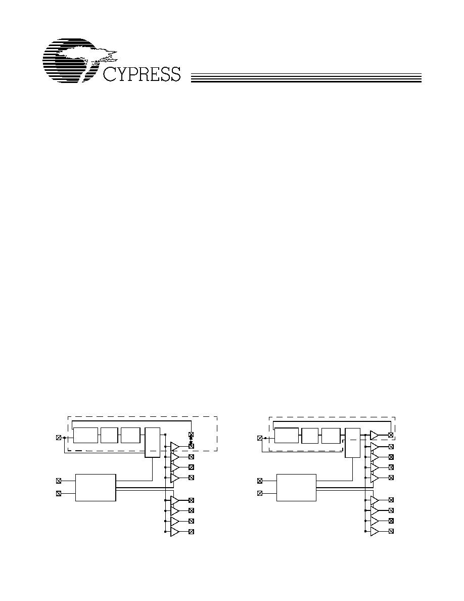
A simplified diagram of the CY2308 zero delay buffer is shown
in Figure 1. The CY2308 is built using a PLL that uses a ref-
erence input and a feedback input. The feedback loop is
closed by driving the feedback input (FBK) from one of the
outputs. The phase detector in the PLL adjusts the output
frequency of the VCO so that the two inputs have no phase
difference. Since an output is one of the inputs to the PLL,
zero phase difference is maintained from REF to the output
driving FBK. Now if all outputs are uniformly loaded, zero
phase difference will be maintained from REF to all outputs.
This is a simple zero delay buffer. Introducing additional de-
vices (e.g., dividers) between the output and FBK can give
rise to some innovative applications for the PLL, and for fur-
ther information on these refer to the Cypress Application
Note "CY2308 Zero Delay Buffer". Since many buffering ap-
plications require only a simple closure of the feedback loop,
Cypress has designed zero delay buffers with Internal Feed-
back Loops: the CY2305 and CY2309.
What are the CY2305 and CY2309?
Cypress has designed zero delay buffers especially suited for
use with PCI or SDRAM buffering. The CY2305 and CY2309
have been designed with the feedback path integrated for
simpler system design. A simplified block diagram of the
CY2309 zero delay buffer is shown Figure 2. This zero delay
buffer uses a input/output pad on CLKOUT so that the feed-
back signal can be sensed directly from the output itself.
Drive Capability
The CY2305 and CY2309 have high drive outputs designed
to meet the JEDEC SDRAM specifications of 30 pF capaci-
tance on each DIMM clock input.
Since the typical CMOS input is 7 pF and the CY2305/09 are
designed to drive up to 30 pF; this means that up to 4 CMOS
inputs can be driven from a single output of a CY2305/09.
However the output loading on the CY2305/09 must be equal
on all outputs to maintain zero delay from the input.
Power Down
The CY2305 and CY2309 have a unique power-down mode:
if the input reference is stopped, the part automatically enters
a shutdown state, shutting down the PLL and three-stating the
outputs. When the part is in shutdown mode it draws less than
50
µ
A, and can come out of shutdown mode with the PLL
locked in less than 1 ms. This power down mode can also be
entered by three-stating the input reference driver and allow-
ing the internal pull-down to pull the input LOW (the input
does not have to go LOW, it only has to stop).
5 Volt to 3.3 Volt Level Shifting
The CY2305 and CY2309 can act as a 5-volt to 3.3-volt level
shifter. The reference input pad is 5-volt signal-compatible.
Since many system components still operate at 5 volts, this
feature provides the capability to generate multiple 3.3-volt
clocks from a single 5-volt reference clock. This 5-volt sig-
nal-compatibility is only available on the reference pad; the
other input pads on the CY2309 are not 5-volt compatible.
Figure 1. Simplified Block Diagram of CY2308
VCO
REF
CLKA1
CLKA2
CLKA3
CLKA4
FBK
Loop
Filter
Phase
Detector
PLL
MUX
Select Input
Decoding
S2
S1
CLKB1
CLKB2
CLKB3
CLKB4
Figure 2. Simplified Block Diagram of CY2309
VCO
REF
CLKA1
CLKA2
CLKA3
CLKA4
CLKOUT
Loop
Filter
Phase
Detector
PLL
MUX
Select Input
Decoding
S2
S1
CLKB1
CLKB2
CLKB3
CLKB4
CY2305 and CY2309 as PCI and SDRAM Buffers
2
Lead or Lag Adjustments
To adjust the lead or lag of the outputs on the CY2305 or
CY2309, one must understand the relationships between
REF and CLKOUT, and the relationship between CLKOUT
and the other outputs. To understand the relationship, first we
need to understand a few properties of the CY2305 and
CY2309 Phase Locked Loops. The PLL senses the phase of
the CLKOUT pin at a threshold of V
dd
/2 and compares it to
the REF pin at the same V
dd
/2 threshold. All the outputs start
their transition at the same time (including CLKOUT). Chang-
ing the load on an output changes its rise time and therefore
how long it takes the output to get to the V
dd
/2 threshold.
Using these properties to our advantage, we can then adjust
the time when the outputs reach the V
dd
/2 threshold relative
to when the REF input reaches the V
dd
/2 threshold. The CLK-
OUT output however cannot be adjusted: it will always have
zero delay from the REF input at V
dd
/2. The outputs can be
advanced by loading the CLKOUT output more heavily than
the other outputs or can be delayed by loading CLKOUT more
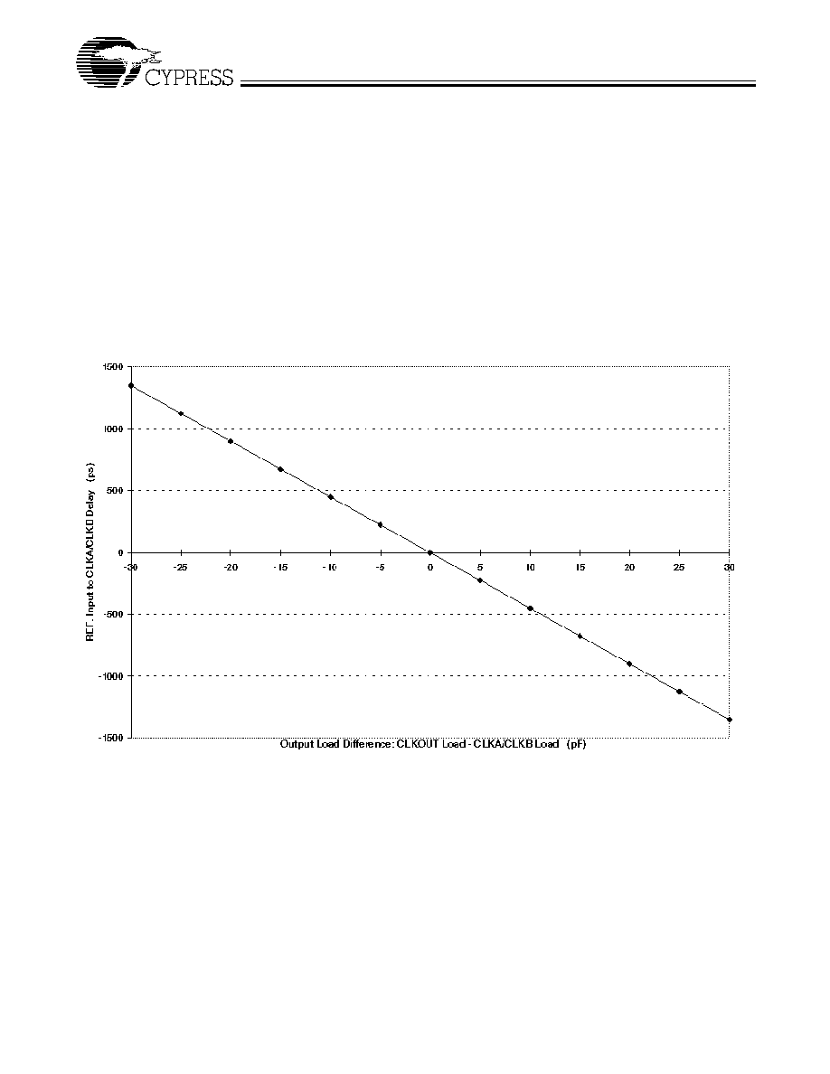
lightly than the other outputs. Figure 3 shows how many ps
the outputs are moved vs. the difference in the loading be-
tween CLKOUT and the other outputs. As a rough guideline,
the adjustment is 50 ps/pF of loading difference. Note: the
zero delay buffer will always adjust itself to keep the V
dd
/2
point of the output at zero delay from the V
dd
/2 point of the
reference. If the application requires the outputs of the zero
delay buffer to have zero delay from another output of the
reference clock chip, the output of the clock chip that is driving
the zero delay buffer must be loaded the same as the other
outputs of the clock chip or the outputs of the zero delay buffer
will be advanced/delayed with reference to those other out-
puts.
Figure 3. Lead Lag Adjustments
CY2305 and CY2309 as PCI and SDRAM Buffers
3
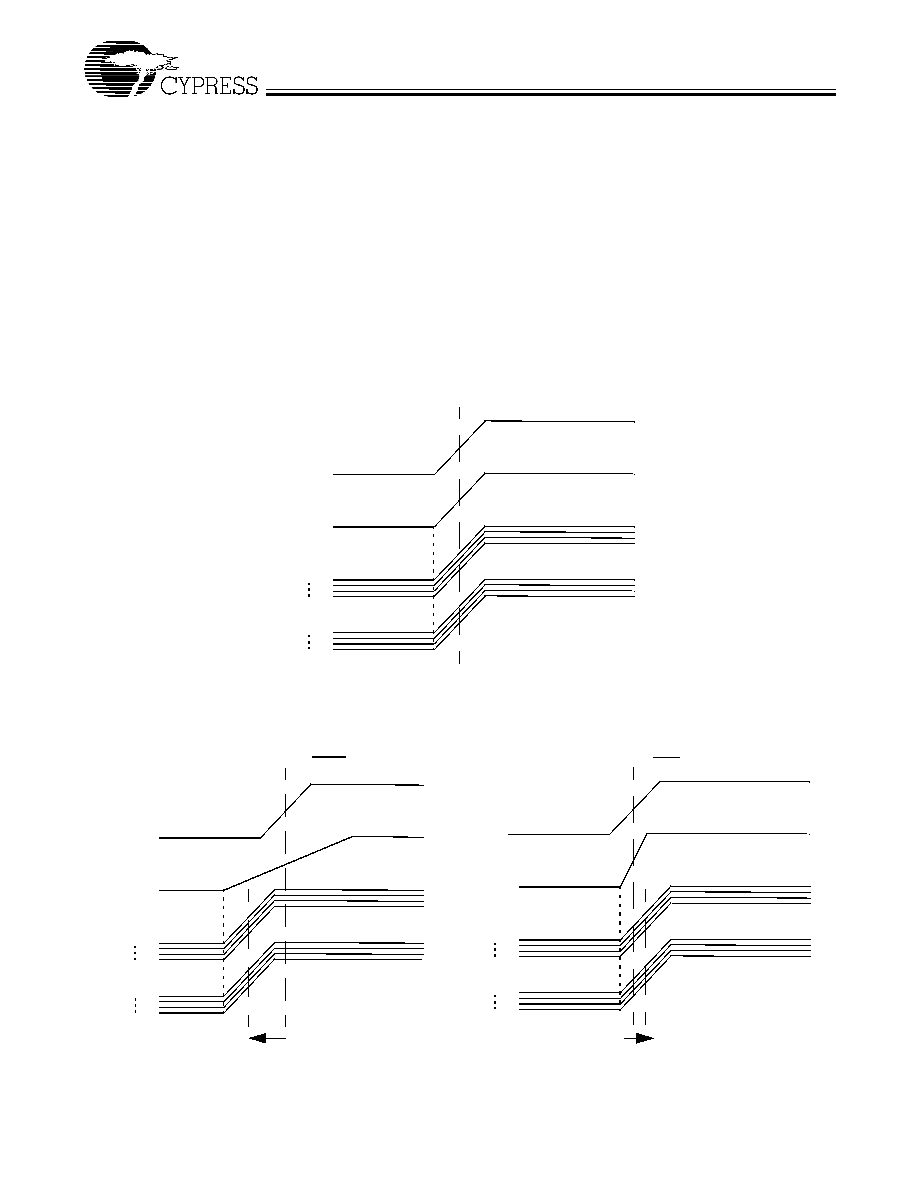
Output To Output Skew
The skew between CLKOUT and the other outputs is not dy-
namically adjusted by the loop. All MUST have the same load
on them to achieve zero output to output skew. If the other
outputs are less loaded than CLKOUT, they will lead it; and if
the other outputs are more loaded, they will lag the CLKOUT.
The relationship that exists between the CLKOUT and the rest
of the outputs is that they all start the rising edge at the same
time, but different loads will cause them to have different rise
times and different times crossing the measurement thresh-
olds. Since CLKOUT is the only output that is monitored, it will
be the output that has the zero delay from the reference and
the other clocks will be relative to CLKOUT and their loading
differences.
Zero Delay Buffer Timing diagrams with different loading configurations.
REF input and all
REF
CLKOUT
CLKA1
CLKA4
outputs loaded equally
REF input and CLKA1-CLKB4 loaded
equally, with CLKOUT loaded less
REF input and CLKA1-CLKB4 loaded
REF
CLKOUT
equally, with CLKOUT loaded more
Advanced
REF
CLKOUT
Delayed
Zero Delay
CLKB1
CLKB4
CLKA1
CLKA4
CLKB1
CLKB4
CLKA1
CLKA4
CLKB1
CLKB4
CY2305 and CY2309 as PCI and SDRAM Buffers
4
Product Information
The CY2305 Zero Delay Buffer
The CY2305 is a 3.3-volt, five output zero delay buffer in an
8-pin 150-mil SOIC package. This part is intended for buffer-
ing one clock into five clocks for PCI buffering or four clocks
for use with 1 SDRAM module. The CY2305 is the simplest
and easiest to use part in the Cypress zero delay buffer family.
For a discussion of the special features of the CY2305 see
the special features section of this application note, or for the
complete specifications on the CY2305 please refer to the
CY2305/CY2309 data sheet.
The CY2309 Zero Delay Buffer
The CY2309 is a 3.3-volt, nine output zero delay buffer in a
16-pin 150-mil SOIC package. This part is intended for buff-
ering one clock into 9 clocks for PCI buffering or eight clocks
for use with 2 SDRAM modules. For the complete specifica-
tions please refer to the CY2305/CY2309 data sheet.
The CY2309 has several options for shutting down the output
banks or completely shutting down the part to conserve pow-
er. As shown in the table below, the inputs S1 and S2 control
which output banks are driven and the state of the PLL. You
will notice that the CLKOUT output is always driven. This is
because the PLL must have the CLKOUT pin running in order
to maintain phase lock. The CY2309 will also go into a power
down state if the input reference stops as described in the
"Special Features of the Cypress Zero Delay Buffers" section.
VCO
REF
CLK1
CLK2
CLK3
CLK4
CLKOUT
LP
Filter
Phase
Detector
PLL
1
2
3
4
5
8
7
6
REF
CLK2
CLK1
GND
V
DD
CLKOUT
CLK4
CLK3
SOIC
Top View
VCO
EF
CLKA1
CLKA2
CLKA3
CLKA4
CLKOUT
LP
Filter
Phase
Detector
PLL
MUX
Select Input
Decoding
S2
S1
CLKB1
CLKB2
CLKB3
CLKB4
1
2
3
4
13
16
15
14
REF
CLKA1
CLKA2
V
DD
CLKA3
CLKOUT
CLKA4
V
DD
SOIC
Top View
5
6
7
8
GND
CLKB1
CLKB2
S2
9
12
11
10
CLKB3
GND
CLKB4
S1
Select Input Decoding for CY2309
S2
S1
CLOCK A1≠A4
CLOCK B1≠B4
CLKOUT
[1]
Output Source
PLL Shutdown
0
0
Three-State
Three-State
Driven
PLL
N
0
1
Driven
Three-State
Driven
PLL
N
1
0
Driven
Driven
Driven
Reference
Y
1
1
Driven
Driven
Driven
PLL
N
Note:
1. This output is driven and has an internal feedback for the PLL. The load on this output can be adjusted to change the delay between the
reference and the CLKA/CLKB outputs.
CY2305 and CY2309 as PCI and SDRAM Buffers
5
Applications
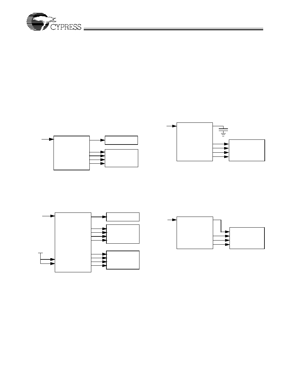
5 and 9 PCI Device/Slot Zero Delay Buffer Solution
The CY2305 and CY2309 are an excellent clocking solution
for a system that requires more PCI clocks than the currently
popular clock chips provide. The CY2305 comes in a tiny
150-mil 8-pin SOIC package and the CY2309 comes in a
small 150-mil 16-pin SOIC package. The CY2305 and
CY2309 are priced very aggressively for the high volume PC
market. There are two solutions for implementing a PCI zero
delay buffer with the Cypress zero delay buffers: a 5 de-
vice/slot and a 9 device/slot buffer.
The 5 Device/Slot Solution:
∑ PCI/Slot 1 (CLKOUT) must always be loaded.
∑ If PCI Slots represent different loads, they will have earlier
or later clocks (See Lead or Lag Adjustments section of
"Special Features of Cypress Zero Delay Buffers".
The 9 Device/Slot Solution:
∑ PCI/Slot 1 (CLKOUT) must always be loaded.
∑ Select lines can be used to shut down output banks, see
CY2309 data sheet.
1 SDRAM DIMM Zero Delay Buffer Solution
The CY2305 is an excellent clocking solution for a system
using 1 SDRAM DIMM. The CY2305 comes in a very small
150-mil 8-pin SOIC package and is priced very aggressively
for the high volume PC market. There are two solutions for
implementing 1 SDRAM DIMM support with the CY2305: the
first is the adjustable delay solution, and the second is the self
adjusting delay solution.
The Adjustable Delay Solution:
∑ C
load
must be equal to SDRAM module loading for zero
delay.
∑ To make the SDRAM inputs lead or lag the reference input
see the Lead or Lag Adjustments section of "Special Fea-
tures of the Cypress Zero Delay Buffers".
The Self Adjusting Solution:
∑ This solution will automatically compensate for different
SDRAM input loads.
∑ CLKOUT must drive CK0 on the SDRAM module so that
CLKOUT is always fully loaded (pin 42 on the SDRAM
module).
CY2305
Zero Delay
Buffer
PCICLK
CLK4
REF
CLK3
CLK2
CLK1
4 PCI Devices/Slots
CLKOUT
PCI Device 1
CY2309
Zero Delay
Buffer
PCICLK
CLKA4
REF
CLKA3
CLKA2
CLKA1
4 PCI Devices/Slots
CLKOUT
PCI Device 1
CLKB1
4 PCI Devices/Slots
CLKB2
CLKB3
CLKB4
S1
S2
V
dd
CY2305
SDRAM Module
Zero Delay
Buffer
CPUCLK
CLK4
CLK3
CLK2
CLK1
CLKOUT
REF
C
load
CY2305
SDRAM Module
Zero Delay
Buffer
CPUCLK
CLK4
CLK3
CLK2
CLK1
REF
CLKOUT